 | –≠–ª–µ–∫—Ç—Ä–æ–Ω–Ω—ã–π –∫–æ–º–ø–æ–Ω–µ–Ω—Ç: L6611DTR | –°–∫–∞—á–∞—Ç—å:  PDF PDF  ZIP ZIP |
1/28
L6611
April 2002
s
OV/UV DETECTION FOR 3.3V, +5V, ±12V
RAILS AND 5V (OR 3.3V) AUX. VOLTAGE
s
AC MAINS UV (BROWNOUT) DETECTION
WITH HYSTERESIS
s
ON-LINE DIGITAL TRIMMING FOR 5V/12V,
3.3V, 5V (OR 3.3V) AUX. FEEDBACK
REFERENCES AND AC MAINS UV.
s
DIGITALLY SELECTABLE OPTIONS
s
ERROR AMPLIFIERS FOR 5V/12V RAILS
(MAIN SUPPLY), 3V3 POST-REGULATOR
(MAG_AMP OR LINEAR) AND AUXILIARY
SUPPLY.
s
MAIN SUPPLY ON/OFF CONTROL AND
POWER GOOD SIGNAL
s
50mA CROWBAR DRIVE FOR AUXILIARY
OUTPUT OVP.
s
OPEN GROUND PROTECTION
s
8ms DIGITAL SOFT START
s
64 ms UV/OC BLANKING AT START-UP
APPLICATIONS
s
SWITCHING POWER SUPPLIES FOR
DESKTOP PC'S, SERVERS AND WEB
SERVERS
s
SUPERVISOR FOR DISTRIBUTED POWER
DIP20
SO20
ORDERING NUMBERS:
L6611N
L6611D
L6611DTR(T & Reel)
DIGITALLY PROGRAMMABLE SECONDARY
HOUSEKEEPING CONTROLLER
TYPICAL APPLICATION CIRCUIT
+5Vaux
WIDE RANGE
MAINS
+5V
COM
+3.3V
+12V
-
+
MAIN
CONTROL
AUXILIARY
CONTROL
VDD
12V
Cout
Gnd
MFault
Aout
5V
3V3
L6611
-12V
-12V
Dmon
Bout
BCD TECHNOLOGY

L
6611
2/28
BL
O
C
K D
I
AG
RA
M
+3
V
3
+
12V
Vd
d
OV
Logic and Programmable Trimming
Pr
o
g
Ci
n
v
Co
u
t
Dmo
n
Vd
d
2
.
5
0V(B)
uv
ov
OC
P
B
ounc
e
L
Vd
d
V
U
f
Re
se
t
1
.
25
V
(
A)
2.
50
V(
A
)
V
r
e
2.
50
V(
B)
D
e
b
oun
c
e
75
m
s
2.
50
V(
C
)
10
m
A
Gn
d
B
out
A
out
Bi
n
v
Ai
n
v
S
o
f
t
St
art
2.
50
V(A)
+
5
V
+
12V
1
.
25
V
(
B)
ov
D
i
s
abl
e
uv
ov
uv
uv
ov
ov
uv
2.
50
V(B)
D
f
ault
P
S
-
O
N /
Cl
o
c
k
Vr
e
g
P
W
-
O
K
/ D
a
ta
M
f
aul
t
AC
s
n
s
-1
2V
+
12V
+5
V
+5
V
+
3V3
5
0uA
ov
Vd
d
P
r
ogra
m
m
i
ng inp
u
t
+/
-
1
2
V
U
V
3
V3 +
5V U
V
UV
Vd
d
+
_
2.
50
V(B)
2.
50
V(
C
)
1.
2
5V(
A
)
1.
2
5V(B
)
V
-
-
-
+
_
3/28
L6611
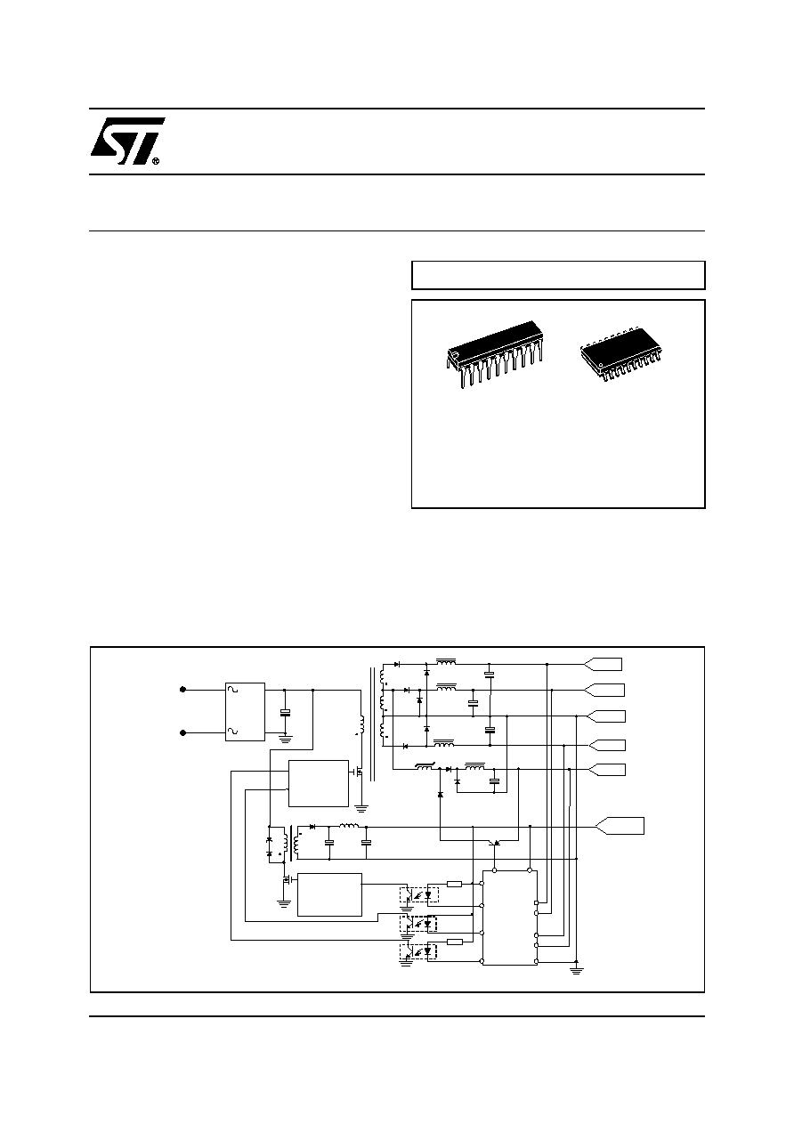
DESCRIPTION
The L6611 is a control and housekeeping IC developed in BCD technology; it is intended for acting at the sec-
ondary side of desktop PC's or server's switching power supplies, in presence of standard voltage rails (+3.3V,
+5V, ±12V) generated by a main converter and of a supply line generated by an auxiliary converter. The typical
application circuit is showed on the front page.
The Housekeeping's main function is to control and monitor the voltages generated by both the main and the
auxiliary converter: it senses those voltages, sends feedback signals to the primary controllers for regulation
and, upon detection of an undervoltage (UV), or overvoltage (OV) condition, reports such fault and takes proper
action to protect the system.
However, the peculiar feature of this IC is its digital programming capability that enables an accurate trimming
of the output voltage rails during production test via software, without any use of external discrete trimming com-
ponents or need for manual intervention on the PSU. It is also possible to program some of the monitoring func-
tions and select how UV and OC conditions are handled in the main converter: whether latched-mode (the
information is latched and released only by forcing the restart of the IC) or bouncing-mode (an attempt is made
to automatically restart the converter after 1 second wait).
A key feature of this IC is its contribution to a very low external component count. Besides the extensive use of
onboard programmable switches, which prevents the need for external trimming components, the IC embeds
reference voltages, error amplifiers and most of the housekeeping circuitry normally required.
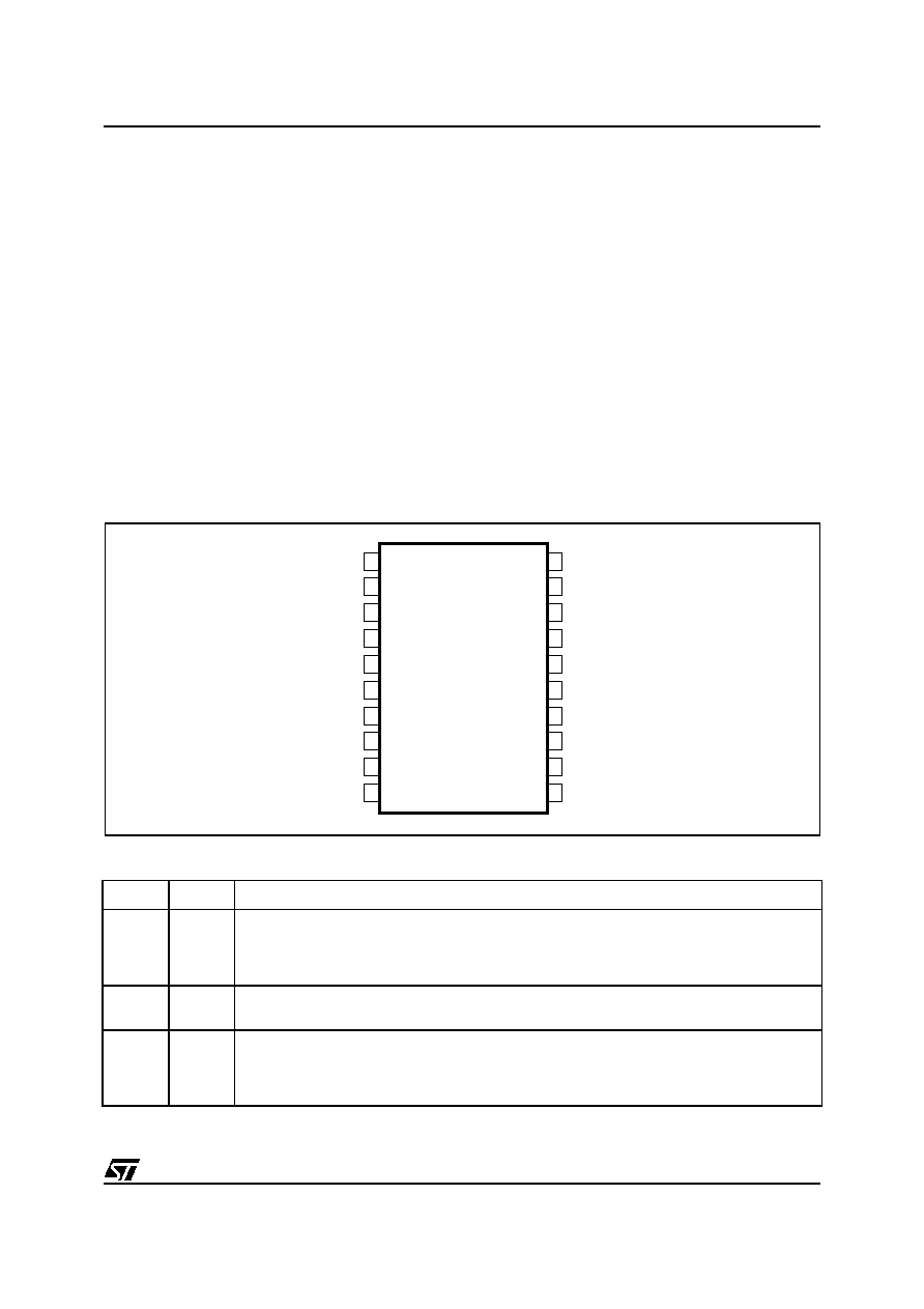
PIN CONNECTION (top view)
PIN DESCRIPTION
Pin #
Name
Description
1
MFAULT
Main converter on/off control. This pin is a 10mA current sink used for driving an opto-isolator. It
is normally low when PS-ON (#13) is pulled low. If a fault is detected or PS-ON goes high, this
pin goes high too. To allow power up, the functions are digitally blanked out for a period (UVB
function) and MFAULT (#1) stays low. There is no delay for the OV protection function.
2
Binv
Inverting input to the error amplifier for the 3V3 post-regulator (either mag-amp or linear). The
non-inverting input is connected to an internal 1.25V reference that can be digitally trimmed.
3
Bout
Output of the 3V3 error amplifier. It typically drives either a PNP transistor that sets the mag-amp
core or the pass element of a linear regulator. Also node for error amplifier compensation. The
maximum positive level of this output is clamped at about 3.5V to improve response time. Large
signal slew rate is limited to reduce noise sensitivity.
MFAULT
Binv
Bout
12V
5V
3V3
-12V
VREF
PS-ON
PW-OK
ACsns
Vdd
DFAULT
Dmon
Cout
Aout
Ainv
PROG
Cinv
GND
-
-
MFAULT
Binv
Bout
12V
5V
3V3
-12V
VREF
PS-ON
PW-OK
ACsns
Vdd
DFAULT
Dmon
Cout
Aout
Ainv
PROG
Cinv
GND
-
-

L6611
4/28
4
Aout
Output of the error amplifier for the main converter. This pin typically drives an optocoupler and is
also used for compensation along with Ainv (pin #5).
5
Ainv
Main loop error amplifier inverting input. The non-inverting input is connected to an internal 2.5V
reference that can be digitally trimmed. A high impedance internal divider from +12V and +5V
UV/OV sense pins (#19, #20) eliminates the need for external divider in most applications. The
pin is used for error amplifier compensation.
6
Cout
Auxiliary loop optocoupler drive. Also node for error amp compensation. Large signal slew rate is
limited to reduce sensitivity to switching noise.
7
Cinv
Inverting input for Auxiliary error amplifier. The non-inverting input is connected to an internal
1.25V reference that can be digitally trimmed.
8
Dmon
Dual or Auxiliary UV/OV monitor, Dmon is programmable to monitor 3V3 or 5V. To allow a correct
power up, the UV function on this pin is blanked out during initial start-up. There is no delay for
the OV function.
9
DFAULT
Dual or Auxiliary fault protection. When Dmon (#8) recognizes an over voltage, DFAULT and
MFAULT (#1) go high. DFAULT is capable of sourcing up to 50mA. Possible applications are a
crowbar across the Auxiliary output or an opto-coupled fault signal to the primary side.
10
Vdd
Positive input supply voltage. Vdd is normally supplied from the Auxiliary power supply output
voltage. If Vdd-UVL detects a sustained under voltage, PW-OK (#12) will be pulled low and
sending MFAULT (#1) high will disable the main converter.
11
ACsns
Analog of bulk voltage for AC fail warning. The usual source of this analog pin is one of the
secondary windings of the main transformer. Hysteresis is provided through a trimmable 50
µ
A
current sink on this pin that is activated as the voltage at the pin falls below the internal reference
(2.5V).
12
PW-OK
/Data
Power good signal for the Main converter. When asserted high, this pin indicates that the
voltages monitored are above their UV limits. There will be typically 250ms delay from the Main
outputs becoming good and PW-OK being asserted. This is nominally an open drain signal. To
improve robustness, this output has a limited current sink capability. In programming mode, this
pin is used for data input; then the absolute maximum rating will be Vdd+0.5V.
13
PS-ON /
Clock
Control pin to enable the Main converter. This pin has debouncing logic. A recognized high value
on this pin will cause PW-OK (#12) to go immediately low and, after a delay of 2.5ms, to shut
down the main PWM by allowing MFAULT (#1) to go high. During normal operation (or if not
used) this pin has to be connected to a voltage lower than 0.8V. In programming mode, this pin
will be used to clock serial data into the chip.
14
VREF
2.5V reference for external applications. This is a buffered pin. Shorting this pin to ground or to
Vdd (#10) will not affect integrity of control or monitor references. An external capacitor (max.
100nF) is required whenever the pin is loaded (up to 5 mA), otherwise it can be left floating.
15
-12V
-12V UV/OV monitor. If connected to a voltage greater than 1.5V (e.g. VREF, #14), the function
will be disabled.
16
GND
Ground pin. The connection integrity of this pin is constantly monitored and in case of either a
bond wire or a PCB trace going open, MFAULT (#1) and DFAULT (#9) will be forced high
switching off the supply.
17
PROG
The chip has 2 operating modes, depending on PROG input pin biasing:
≠
normal mod
e: PROG should be floating or shorted to ground;
≠
programming mod
e: forcing PROG high (+5V), the chip enters programming mode. PW_OK
(#12) and PS_ON (#13) pins are disconnected from their normal functionality and they become
inputs for DATA and CLOCK allowing the chip to be programmed. The programming mode al-
lows selecting some options and adjusting some setpoints;
PIN DESCRIPTION (continued)
Pin #
Name
Description

5/28
L6611
18
3V3
3V3 UV/OV monitor. It uses a separate reference to the feedback reference.
19
5V
Input pin for 5V feedback, 5V current sense and 5V UV/OV monitor. 5V UV/OV uses a reference
separate from that used for feedback. This pin connects the 5V part of the Main error amplifier
feedback divider.
20
12V
Input pin for 12V feedback, 12V current sense and 12V UV/OV monitor.12V UV/OV uses a
reference separate from that used for feedback. This pin connects the 12V part of the Main error
amplifier feedback divider.
FUNCTION DESCRIPTION
Name
Description
OVP
Whenever one of the Main output voltages is detected going above its own OVP threshold, this
function set MFAULT (#1) high latching the outputs off. The latch is released after cycling PS-ON
(#13) switch or by reducing Vdd (#10) below the UV threshold.
UVP
Whenever one of the Main output voltages is detected going under its own UVP threshold, this
function sets MFAULT (#1) high; if latch mode has been selected, this function will be latched.
Otherwise an attempt will be made to restart the device after 1 second delay. If ACsns (#11) is
low due to a brownout condition, UVP is disabled.
UVB
Undervoltage blanking. When either converter is enabled, the relevant UV/OC monitoring circuits
must not intervene to allow all outputs to come within tolerance. 64 ms timing is provided; for the
auxiliary converter the timing starts as the IC has a valid supply, for the main converter it starts
as the ACsns pin detects a valid input voltage for the converter.
PW-OK delay
PW-OK delay. After power-up, when the all of the monitored voltages are above their own UV
threshold the PW-OK pin (#12) will be kept low for additional 250ms (typ.) to make sure all the
outputs are settled.
OFF delay
Power-off delay. As soon as PS-ON (#13) pin is recognized high, indicating an imminent turn-off
condition, PW-OK (#12) pin will go low immediately . The converter will be turned off after a
delay of 2.5ms.
Debounce
The PS-ON signal input has debounce logic to prevent improper activation. All of the monitored
inputs have digital filtering/debounce logic on board for high noise immunity.
AC-hysteresis
AC sense hysteresis. Programmable hysteresis is provided on the ACsns input (#11) to avoid
undesired shutdown caused by noise as the voltage at the pin is near the threshold or by the
voltage ripple across the bulk capacitor.
Vdd-OVP
Vdd is monitored for overvoltage. If an overvoltage is detected, MFAULT (#1) and DFAULT (#9)
are latched high.
Vdd-UVL
To prevent false signals of any of IC's output pins, an under voltage lock-out circuit monitors Vdd
and keeps all IC's output at their default OFF level until Vdd reaches a sufficient minimum
voltage for ensuring integrity. When Vdd goes below the UV threshold, all latches are reset and
volatile programming memory cleared.
Dual-OVP
Dmon (#8) is monitored to detect an overvoltage condition; in this case MFAULT (#1) and
DFAULT (#9) are latched high.
Dual-UVP
Dmon (#8) is monitored to detect an undervoltage condition; in this case MFAULT (#1) is latched
high and Cout (#6) is pulled low.
PIN DESCRIPTION (continued)
Pin #
Name
Description