 | –≠–ª–µ–∫—Ç—Ä–æ–Ω–Ω—ã–π –∫–æ–º–ø–æ–Ω–µ–Ω—Ç: L6918D | –°–∫–∞—á–∞—Ç—å:  PDF PDF  ZIP ZIP |

1/35
L6918 L6918A
October 2002
s
OUTPUT CURRENT IN EXCESS OF 100A
s
ULTRA FAST LOAD TRANSIENT RESPONSE
s
REMOTE SENSE BUFFER
s
INTEGRATED 2A GATE DRIVERS
s
5 BIT VID VOLTAGE POSITIONING, VRM 9.0
s
0.6% INTERNAL REFERENCE ACCURACY
s
DIGITAL 2048 STEP SOFT-START
s
OVP & OCP PROTECTIONS
s
Rdson or Rsense CURRENT SENSING
s
1200KHz EFFECTIVE SWITCHING
FREQUENCY, EXTERNALLY ADJUSTABLE
s
POWER GOOD OUTPUT AND INHIBIT
s
PACKAGE: SO28
APPLICATIONS
s
HIGH DENSITY DC-DC FOR SERVERS AND
WORKSTATIONS
s
SUPPLY FOR HIGH CURRENT
MICROPROCESSORS
s
DISTRIBUTED POWER
DESCRIPTION
L6918A is a master device that it has to be combined
with the L6918,slave, realizing a 4-phases topology,
interleaved. The device kit is specifically designed to
provide a high performance/high density DC/DC con-
version for high current microprocessors and distrib-
uted power. Each device implements a dual-phase
step-down controller with a 180∞ phase-shift between
each phase.
A precise 5-bit DAC allows adjusting the output volt-
age from 1.100V to 1.850V with 25mV binary steps.
The high peak current gate drives affords to have
high system switching frequency, typically of
1200KHz, and higher by external adjustement.
The device kit assure a fast protection against OVP,
UVP and OCP. An internal crowbar, by turning on the
low side mosfets, eliminates the need of external pro-
tection. In case of over-current, the system works in
Constant Current mode.
SO28
ORDERING NUMBERS: L6918D, L6918AD
L6918DTR, L6918ADTR
5 BIT PROGRAMMABLE MULTIPHASE CONTROLLER
PIN CONNECTIONS
1
3
2
4
5
6
7
8
9
18
17
16
15
19
20
10
11
12
13
14
24
23
22
21
25
26
27
28
LGATE1
VCCDR
PHASE1
FB
BOOT1
UGATE1
VSEN
VCC
SGND
COMP
ISEN1
PGNDS1
FBR
FBG
SYNC_IN
SLAVE_OK
SYNC / ADJ
VPROG_IN
BOOT2
PGOOD
UGATE2
PHASE2
LGATE2
PGND
OSC / INH / FAULT
ISEN2
PGNDS2
SYNC_OUT
L
6
918
(S
la
v
e
)
1
3
2
4
5
6
7
8
9
18
17
16
15
19
20
10
11
12
13
14
24
23
22
21
25
26
27
28
LGATE1
VCCDR
PHASE1
FB
BOOT1
UGATE1
VPROG_OUT
VCC
SGND
COMP
ISEN1
PGNDS1
SYNC_OUT
SLAVE_OK
VID3
VID2
VID1
VID4
BOOT2
PGOOD
UGATE2
PHASE2
LGATE2
PGND
OSC / INH / FAULT
ISEN2
PGNDS2
VID0
L
6
91
8A
(
Ma
s
t
e
r
)

L6918 L6918A
2/35
L6918A (MASTER) DEVICE BLOCK DIAGRAM
L6918 (SLAVE) DEVICE BLOCK DIAGRAM
UGATE1
CURRENT
READING
I
FB
TO TAL
CUR RENT
CUR
R
E
NT
AV
G
CH1
OCP
DAC
DIGITAL
SO FT- STAR T
LO
G
I
C
P
W
M
AD
AP
T
I
VE
AN
T
I
CR
O
S
S
C
O
ND
U
C
T
I
O
N
CH1 OCP
2
PH
A
SE
O
S
C
I
LLA
T
O
R
P WM1
CU
RRE
N
T
C
O
R
R
E
C
TIO
N
ERROR
AMPLIFIER
LS
LS
HS
Vc c
HS
BOOT1
PHAS E1
LGATE1
ISEN1
PGNDS1
PGND
PGNDS2
ISEN2
LGATE2
PHAS E2
UGATE2
BOOT2
Vcc
COMP
FB
VSEN
VID0
VID1
VID2
VID3
VID4
ROSC / INH
SGND
VCCDR
VCC DR
VCC
LO
G
I
C
A
N
D
P
R
OT
E
C
T
I
ON
S
CH2 OCP
P WM2
CU
RRE
N
T
C
O
R
R
E
C
TIO
N
CH2
OCP
CURRENT
READING
LO
G
I
C
P
W
M
A
D
AP
T
I
VE
AN
T
I
CR
O
S
S
C
O
ND
U
C
T
I
O
N
PGOOD
SYNCH.
CIRCUITRY
SYNC_ OUT
SLAVE_OK
UGATE1
CURRENT
READING
CURRENT
READING
I
FB
TO TAL
CUR RENT
CUR
R
E
NT
AV
G
CH1
OCP
DAC
DIGITAL
SO FT- STAR T
LO
G
I
C
P
W
M
AD
AP
T
I
VE
AN
T
I
CR
O
S
S
C
O
ND
U
C
T
I
O
N
LO
G
I
C
P
W
M
AD
AP
T
I
VE
AN
T
I
CR
O
S
S
C
O
ND
U
C
T
I
O
N
CH1 OCP
2
PH
A
SE
O
S
C
I
LLA
T
O
R
P WM1
CU
RRE
N
T
C
O
R
R
E
C
TIO
N
ERROR
AMPLIFIER
LS
LS
HS
Vc c
HS
BOOT1
PHAS E1
LGATE1
ISEN1
PGNDS1
PGND
PGNDS2
ISEN2
LGATE2
PHAS E2
UGATE2
BOOT2
Vcc
COMP
FB
VSEN
VID0
VID1
VID2
VID3
VID4
ROSC / INH
SGND
VCCDR
VCC DR
VCC
LO
G
I
C
A
N
D
P
R
OT
E
C
T
I
ON
S
CH2 OCP
P WM2
CU
RRE
N
T
C
O
R
R
E
C
TIO
N
CH2
OCP
CURRENT
READING
CURRENT
READING
LO
G
I
C
P
W
M
A
D
AP
T
I
VE
AN
T
I
CR
O
S
S
C
O
ND
U
C
T
I
O
N
LO
G
I
C
P
W
M
A
D
AP
T
I
VE
AN
T
I
CR
O
S
S
C
O
ND
U
C
T
I
O
N
PGOOD
SYNCH.
CIRCUITRY
SYNC_ OUT
SLAVE_OK
UGATE1
CURRENT
READING
I
FB
TO TAL
CUR RENT
CURR
E
N
T
AV
G
CH1
OCP
LO
G
I
C
P
W
M
AD
AP
T
I
V
E
AN
T
I
C
R
O
S
S
CO
N
DUC
T
I
O
N
CH1 OCP
2 P
H
A
S
E
O
S
C
I
LLA
T
O
R
P WM1
CU
RRE
N
T
CO
R
R
E
CTI
O
N
ERROR
AMPLIFIER
LS
LS
HS
Vc c
HS
BOOT1
PHAS E1
LGATE1
ISEN1
PGNDS1
PGND
PGNDS2
ISEN2
LGATE2
PHAS E2
UGATE2
BOOT2
Vcc
COMP
FB
V SEN
ROSC / INH
SGND
VCCDR
VCC DR
VCC
LO
G
I
C
A
N
D
PR
O
T
E
C
T
I
O
N
S
CH2 OCP
P WM2
CU
RRE
N
T
CO
R
R
E
CTI
O
N
CH2
OCP
CURRENT
READING
LO
G
I
C
P
W
M
A
D
AP
T
I
V
E
AN
T
I
C
R
O
S
S
CO
N
DUC
T
I
O
N
PGOOD
SYNC_OUT
SLAV E_OK
RE MOTE
BUFFER
10 k
10 k
1 0k
VSEN
FBG
FBR
1 0k
VPROG_IN
SYNC_I N
SLAVE / ADJ
SYNCH.
CIRCUITRY
UGATE1
CURRENT
READING
CURRENT
READING
I
FB
TO TAL
CUR RENT
CURR
E
N
T
AV
G
CH1
OCP
LO
G
I
C
P
W
M
AD
AP
T
I
V
E
AN
T
I
C
R
O
S
S
CO
N
DUC
T
I
O
N
LO
G
I
C
P
W
M
AD
AP
T
I
V
E
AN
T
I
C
R
O
S
S
CO
N
DUC
T
I
O
N
CH1 OCP
2 P
H
A
S
E
O
S
C
I
LLA
T
O
R
P WM1
CU
RRE
N
T
CO
R
R
E
CTI
O
N
ERROR
AMPLIFIER
LS
LS
HS
Vc c
HS
BOOT1
PHAS E1
LGATE1
ISEN1
PGNDS1
PGND
PGNDS2
ISEN2
LGATE2
PHAS E2
UGATE2
BOOT2
Vcc
COMP
FB
V SEN
ROSC / INH
SGND
VCCDR
VCC DR
VCC
LO
G
I
C
A
N
D
PR
O
T
E
C
T
I
O
N
S
CH2 OCP
P WM2
CU
RRE
N
T
CO
R
R
E
CTI
O
N
CH2
OCP
CURRENT
READING
CURRENT
READING
LO
G
I
C
P
W
M
A
D
AP
T
I
V
E
AN
T
I
C
R
O
S
S
CO
N
DUC
T
I
O
N
LO
G
I
C
P
W
M
A
D
AP
T
I
V
E
AN
T
I
C
R
O
S
S
CO
N
DUC
T
I
O
N
PGOOD
SYNC_OUT
SLAV E_OK
RE MOTE
BUFFER
10 k
10 k
1 0k
VSEN
FBG
FBR
1 0k
VPROG_IN
SYNC_I N
SLAVE / ADJ
SYNCH.
CIRCUITRY

3/35
L6918 L6918A
ABSOLUTE MAXIMUM RATINGS
THERMAL DATA
Symbol
Parameter
Value
Unit
Vcc, V
CCDR
To PGND
15
V
V
BOOT
-V
PHASE
Boot Voltage
15
V
V
UGATE1
-V
PHASE1
V
UGATE2
-V
PHASE2
15
V
LGATE1, PHASE1, LGATE2, PHASE2 to PGND
-0.3 to Vcc+0.3
V
VID0 to VID4
-0.3 to 5
V
All other pins to PGND
-0.3 to 7
V
V
PHASEx
Sustainable Peak Voltage t<20nS @ 600kHz
26
V
Symbol
Parameter
Value
Unit
R
th j-amb
Thermal Resistance Junction to Ambient
60
∞
C / W
T
max
Maximum junction temperature
150
∞
C
T
storage
Storage temperature range
-40 to 150
∞
C
T
j
Junction Temperature Range
0 to 125
∞
C
P
MAX
Max power dissipation at Tamb=25
∞
C
2
W
L6918A (MASTER) PIN FUNCTION
N. Name
Description
1
LGATE1
Channel 1 low side gate driver output.
2
VCCDR
LS Mosfet driver supply. 5V or 12V buses can be used.
3
PHASE1
This pin is connected to the Source of the upper mosfet and provides the return path for the
high side driver of channel 1.
4
UGATE1
Channel 1 high side gate driver output.
5
BOOT1
Channel 1 bootstrap capacitor pin. This pin supplies the high side driver. Connect through a
capacitor to the PHASE1 pin and through a diode to Vcc (cathode vs. boot).
6
VCC
Device supply voltage. The operative supply voltage is 12V.
7
GND
All the internal references are referred to this pin. Connect it to the PCB signal ground.
8
COMP
This pin is connected to the error amplifier output and is used to compensate the control
feedback loop.
9
FB
This pin is connected to the error amplifier inverting input and is used to compensate the
voltage control feedback loop.
A current proportional to the sum of the current sensed in both channel is sourced from this pin
(50
µ
A at full load, 70
µ
A at the Over Current threshold). Connecting a resistor R
FB
between
this pin and VSEN pin allows programming the droop effect.
10
VPROG_OUT Reference voltage output used for voltage regulation.
This pin must be connected together with the slave device VPROG_IN pin.
Filter to SGND with 1nF capacitor (a total 30nF distributed capacitance is allowed).
11
SYNC_OUT
Synchronization output signal. From this pin exits a square - 50% duty cycle - 5Vpp ≠90 deg
phase shifted wave clock signal that the Slave device PLL locks to.
Connect this pin to the Slave SYNC_IN pin.
12
SLAVE_OK
Open-drain input/output used for start-up and to manage protections as shown in the timing
diagram. Internally pulled-up. Connect together with other IC's SLAVE_OK pin. Filter with 1nF
capacitor vs. SGND.

L6918 L6918A
4/35
13
ISEN1
Channel 1 current sense pin. The output current may be sensed across a sense resistor or
across the low-side mosfet RdsON. This pin has to be connected to the low-side mosfet drain
or to the sense resistor through a resistor Rg in order to program the current intervention for
each phase at 140% as follow:
Where 35
µ
A is the current offset information relative to the Over Current condition (offset at
OC threshold minus offset at zero load).The net connecting the pin to the sense point must be
routed as close as possible to the PGNDS1 net in order to couple in common mode any
picked-up noise.
14
PGNDS1
Channel 1 Power Ground sense pin. The net connecting the pin to the sense point must be routed as
close as possible to the ISEN1 net in order to couple in common mode any picked-up noise.
15
PGNDS2
Channel 2 Power Ground sense pin. The net connecting the pin to the sense point must be
routed as close as possible to the ISEN2 net in order to couple in common mode any picked-
up noise.
16
ISEN2
Channel 2 current sense pin. The output current may be sensed across a sense resistor or
across the low-side mosfet Rds
ON.
This pin has to be connected to the low-side mosfet drain
or to the sense resistor through a resistor Rg in order to program the current intervention for
each phase at 140% as follow:
Where 35
µ
A is the current offset information relative to the Over Current condition (offset at
OC threshold minus offset at zero load).
The net connecting the pin to the sense point must be routed as close as possible to the
PGNDS2 net in order to couple in common mode any picked-up noise.
17
OSC/INH
FAULT
Oscillator switching frequency pin. Connecting an external resistor from this pin to GND, the
external frequency is increased according to the equation:
Connecting a resistor from this pin to Vcc (12V), the switching frequency is reduced according
to the equation:
If the pin is not connected, the switching frequency is 300KHz.
Forcing the pin to a voltage lower than 0.8V, the device stop operation and enter the inhibit
state; all mosfets are turned OFF.
18
to
22
VID0-4
Voltage Identification pins. These input are internally pulled-up and TTL compatible. They are
used to program the output voltage as specified in Table 1 and to set the over voltage and
power good thresholds.
Connect to GND to program a `0' while leave floating to program a `1'.
23
PGOOD
This pin is an open collector output and is pulled low if the output voltage is not within the
above specified thresholds. It must be connected with the Slave's PGOOD pin.
If not used may be left floating.
24
BOOT2
Channel 2 bootstrap capacitor pin. This pin supplies the high side driver. Connect through a
capacitor to the PHASE2 pin and through a diode to Vcc (cathode vs. boot).
25
UGATE2
Channel 2 high side gate driver output.
26
PHASE2
This pin is connected to the source of the upper mosfet and provides the return path for the
high side driver of channel 2.
27
LGATE2
Channel 2 low side gate driver output.
28
PGND
Power ground pin. This pin is common to both sections and it must be connected through the closest
path to the low side mosfets source pins in order to reduce the noise injection into the device.
L6918A (MASTER) PIN FUNCTION (continued)
N. Name
Description
I
O C Px
35
µ
A R
g
R
s ens e
--------------------------
=
I
O C Px
35
µ
A R
g
R
s ens e
--------------------------
=
f
S
300KHz
14.82 10
6
R
O SC
K
(
)
-----------------------------
+
=
f
S
300KHz
12.91 10
7
R
O SC
K
(
)
-----------------------------
+
=

5/35
L6918 L6918A
L6918 (SLAVE) PIN FUNCTION
N.
Name
Description
1
LGATE1
Channel 1 low side gate driver output.
2
VCCDR
LS Mosfet driver supply. 5V or 12V buses can be used.
3
PHASE1
This pin is connected to the Source of the upper mosfet and provides the return path for the
high side driver of channel 1.
4
UGATE1
Channel 1 high side gate driver output.
5
BOOT1
Channel 1 bootstrap capacitor pin. This pin supplies the high side driver. Connect through a
capacitor to the PHASE1 pin and through a diode to Vcc (cathode vs. boot).
6
VCC
Device supply voltage. The operative supply voltage is 12V.
7
GND
All the internal references are referred to this pin. Connect it to the PCB signal ground.
8
COMP
This pin is connected to the error amplifier output and is used to compensate the control
feedback loop.
9
FB
This pin is connected to the error amplifier inverting input and is used to compensate the
voltage control feedback loop.
A current proportional to the sum of the current sensed in both channel is sourced from this pin
(50
µ
A at full load, 70
µ
A at the Over Current threshold). Connecting a resistor R
FB
between this
pin and VSEN pin allows programming the droop effect.
10
VSEN
Connected to the output voltage it is able to manage Over & Under-voltage conditions and the
PGOOD signal. It is internally connected with the output of the Remote Sense Buffer for
Remote Sense of the regulated voltage.
If no Remote Sense is implemented, connect it directly to the regulated voltage in order to
manage OVP, UVP and PGOOD.
11
FBR
Remote sense buffer non-inverting input. It has to be connected to the positive side of the load
to perform a remote sense.
If no remote sense is implemented, connect directly to the output voltage (in this case connect
also the VSEN pin directly to the output regulated voltage).
12
FBG
Remote sense buffer inverting input. It has to be connected to the negative side of the load to
perform a remote sense.
Pull-down to ground if no remote sense is implemented.
13
ISEN1
Channel 1 current sense pin. The output current may be sensed across a sense resistor or
across the low-side mosfet Rds
ON.
This pin has to be connected to the low-side mosfet drain or
to the sense resistor through a resistor Rg in order to program the current intervention for each
phase at 140% as follow:
Where 35
µ
A is the current offset information relative to the Over Current condition (offset at
OC threshold minus offset at zero load).
The net connecting the pin to the sense point must be routed as close as possible to the
PGNDS1 net in order to couple in common mode any picked-up noise.
14
PGNDS1
Channel 1 Power Ground sense pin. The net connecting the pin to the sense point must be
routed as close as possible to the ISEN1 net in order to couple in common mode any picked-up
noise.
15
PGNDS2
Channel 2 Power Ground sense pin. The net connecting the pin to the sense point must be
routed as close as possible to the ISEN2 net in order to couple in common mode any picked-up
noise.
I
O C Px
35
µ
A R
g
R
s ens e
--------------------------
=

L6918 L6918A
6/35
16
ISEN2
Channel 2 current sense pin. The output current may be sensed across a sense resistor or
across the low-side mosfet Rds
ON.
This pin has to be connected to the low-side mosfet drain or
to the sense resistor through a resistor Rg in order to program the current intervention for each
phase at 140% as follow:
Where 35
µ
A is the current offset information relative to the Over Current condition (offset at
OC threshold minus offset at zero load).
The net connecting the pin to the sense point must be routed as close as possible to the
PGNDS2 net in order to couple in common mode any picked-up noise.
17
OSC/INH
FAULT
Oscillator switching frequency pin. Connecting an external resistor from this pin to GND, the
external frequency is increased according to the equation:
Connecting a resistor from this pin to Vcc (12V), the switching frequency is reduced according
to the equation:
If the pin is not connected, the switching frequency is 300KHz.
Forcing the pin to a voltage lower than 0.8V, the device stops operation and enters the inhibit
state; all mosfets are turned OFF.
The pin is forced high when an over voltage is detected. This condition is latched; to recover it
is necessary turn off and on VCC.
18
SYNC_OUT
Output synchronization signal. A 60
∞
phase shift signal exits when the device works as a Slave
while no signal exits when the device works as an adjustable.
19
SYNC / ADJ
Slave or Adjustable operation.
Connecting this pin to GND the device becomes an adjustable two-phase controller using an
external reference for its regulation. No soft start is implemented in this condition, so it must be
performed with external circuitry. The device switches using its internal oscillator according to
the frequency set by R
OSC
.
Leaving this pin floating, the device works as a Slave two-phase controller. It uses the
reference sourced from the master device and an internal PLL locks the synchronization signal
sourced from the master device.
20
SLAVE_OK
Open-drain output used for start-up and to manage protections as shown in the timing diagram. Internally
pulled-up. Connect together with other IC's SLAVE_OK pin. Filter with 1nF capacitor vs. SGND.
21
SYNC_IN
Synchronization input signal locked during the slave operation. Connect to the master SYNC_OUT pin.
22
VPROG_IN
Reference voltage input used for voltage regulation.
This pin must be connected together with the other's slave (if present) to the VPROG_OUT pin
of the master device.
Filter to SGND with 1nF capacitor (a total 30nF distributed capacitance is allowed).
If the device works as an Adjustable (SYNC/ADJ to GND), this is the reference used for the regulation.
23
PGOOD
This pin is an open collector output and is pulled low if the output voltage is not within the
above specified thresholds. It must be connected with the master's PGOOD pin.
If not used may be left floating.
L6918 (SLAVE) PIN FUNCTION (continued)
N.
Name
Description
I
O C Px
35
µ
A R
g
R
s ens e
--------------------------
=
f
S
300KHz
14.82 10
6
R
O SC
K
(
)
-----------------------------
+
=
f
S
300KHz
12.91 10
7
R
O SC
K
(
)
-----------------------------
+
=

7/35
L6918 L6918A
24
BOOT2
Channel 2 bootstrap capacitor pin. This pin supplies the high side driver. Connect through a
capacitor to the PHASE2 pin and through a diode to Vcc (cathode vs. boot).
25
UGATE2
Channel 2 high side gate driver output.
26
PHASE2
This pin is connected to the Source of the upper mosfet and provides the return path for the
high side driver of channel 2.
27
LGATE2
Channel 2 low side gate driver output.
28
PGND
Power ground pin. This pin is common to both sections and it must be connected through the closest
path to the low side mosfets source pins in order to reduce the noise injection into the device.
ELECTRICAL CHARACTERISTCS
(Vcc=12V±10%, TJ=0∞C to 70∞C unless otherwise specified)
Symbol
Parameter
Test Condition
Min.
Typ.
Max.
Unit
Vcc SUPPLY CURRENT
I
CC
Vcc supply current
HGATEx and LGATEx open
V
CCDR
=V
BOOT
=12V
7.5
10
12.5
mA
I
CCDR
V
CCDR
supply current
LGATEx open; V
CCDR
=12V
2
3
4
mA
I
BOOTx
Boot supply current
HGATEx open; PHASEx to
PGND
V
CC
=V
BOOT
=12V
0.5
1
1.5
mA
POWER-ON
Turn-On V
CC
threshold
V
CC
Rising; V
CCDR
=5V
7.8
9
10.2
V
Turn-Off V
CC
threshold
V
CC
Falling; V
CCDR
=5V
6.5
7.5
8.5
V
Turn-On V
CCDR
Threshold
V
CCDR
Rising; V
CC
=12V
4.2
4.4
4.6
V
Turn-Off V
CCDR
Threshold
V
CCDR
Falling; V
CC
=12V
4.0
4.2
4.4
V
OSCILLATOR AND INHIBIT
f
OSC
Initial Accuracy
OSC = OPEN
OSC = OPEN; Tj=0
∞
C to 125
∞
C
278
270
300
322
330
kHz
kHz
f
OSC,Rosc
Total Accuracy
R
T
to GND=74k
450
500
550
kHz
Vosc
Ramp Amplitude
2
V
d
MAX
Maximum duty cycle
OSC = OPEN
45
50
-
%
INH
Inhibit threshold
I
SINK
=5mA
0.8
0.85
0.9
V
REFERENCE AND DAC only for L6918A (MASTER)
V
PROG_OUT
Reference Voltage
Accuracy
VID0 to VID4 see Table1
-0.6
-
0.6
%
I
DAC
VID pull-up Current
VIDx = GND
4
5
6
µ
A
VID pull-up Voltage
VIDx = OPEN
3.1
-
3.4
V
ERROR AMPLIFIER
DC Gain
80
dB
SR
Slew-Rate
COMP=10pF
15
V/
µ
S
Offset
-7
7
mV
DIFFERENTIAL AMPLIFIER (REMOTE BUFFER) only for L6918 (SLAVE)
DC Gain
1
V/V
CMRR
Common Mode Rejection Ratio
40
dB
Input Offset
FBR=1.100V to1.850V;
FBG=GND
-12
12
mV
DIFFERENTIAL CURRENT SENSING
I
ISEN1
,
I
ISEN2
Bias Current
I
LOAD
= 0%
45
50
55
µ
A
L6918 (SLAVE) PIN FUNCTION (continued)
N.
Name
Description

L6918 L6918A
8/35
Table 1. VID Settings (only for L6918A)
I
PGNDSx
Bias Current
45
50
55
µ
A
I
ISEN1
,
I
ISEN2
Bias Current at
Over Current Threshold
80
85
90
µ
A
I
FB
Active Droop Current
I
LOAD
= 0
0
1
µ
A
I
LOAD
= 100%
47.5
50
52.5
µ
A
GATE DRIVERS
t
RISE HGATE
High Side
Rise Time
V
BOOTx
-V
PHASEx
=10V;
C
HGATEx
to PHASEx=3.3nF
15
30
nS
I
HGATEx
High Side
Source Current
V
BOOTx
-V
PHASEx
=10V 2
A
R
HGATEx
High Side
Sink Resistance
V
BOOTx
-V
PHASEx
=12V;
1.5
2
2.5
t
RISE LGATE
Low Side
Rise Time
V
CCDR
=10V;
C
LGATEx
to PGNDx=5.6nF
30
55
nS
I
LGATEx
Low Side
Source Current
V
CCDR
=10V
1.8
A
R
LGATEx
Low Side
Sink Resistance
V
CCDR
=12V
0.7
1.1
1.5
PROTECTIONS
PGOOD
Upper Threshold
(V
SEN
/ VPROG_IN)
V
SEN
Rising
109
112
115
%
PGOOD
Lower Threshold
(V
SEN
/ VPROG_IN)
V
SEN
Falling
87
90
93
%
OVP
Over Voltage Threshold
(V
SEN
/ VPROG_IN)
V
SEN
Rising
114
117
120
%
UVP
Under Voltage Trip
(V
SEN
/ VPROG_IN)
V
SEN
Falling
55
60
65
%
V
PGOOD
PGOOD Voltage Low
I
PGOOD
= -4mA
0.3
0.4
0.5
V
VID4 VID3
VID2
VID1
VID0
Output
Voltage (V)
VID4 VID3
VID2
VID1
VID0
Output
Voltage (V)
0
0
0
0
0
1.850
1
0
0
0
0
1.450
0
0
0
0
1
1.825
1
0
0
0
1
1.425
0
0
0
1
0
1.800
1
0
0
1
0
1.400
0
0
0
1
1
1.775
1
0
0
1
1
1.375
0
0
1
0
0
1.750
1
0
1
0
0
1.350
0
0
1
0
1
1.725
1
0
1
0
1
1.325
0
0
1
1
0
1.700
1
0
1
1
0
1.300
0
0
1
1
1
1.675
1
0
1
1
1
1.275
0
1
0
0
0
1.650
1
1
0
0
0
1.250
0
1
0
0
1
1.625
1
1
0
0
1
1.225
0
1
0
1
0
1.600
1
1
0
1
0
1.200
0
1
0
1
1
1.575
1
1
0
1
1
1.175
0
1
1
0
0
1.550
1
1
1
0
0
1.150
0
1
1
0
1
1.525
1
1
1
0
1
1.125
0
1
1
1
0
1.500
1
1
1
1
0
1.100
0
1
1
1
1
1.475
1
1
1
1
1
Shutdown
ELECTRICAL CHARACTERISTCS (continued)
(Vcc=12V±10%, TJ=0∞C to 70∞C unless otherwise specified)
Symbol
Parameter
Test Condition
Min.
Typ.
Max.
Unit

9/35
L6918 L6918A
FOUR PHASE REFERENCE SCHEMATICS
PGOOD
PGND
PGNDS2
ISEN2
LGATE2
PHASE2
UGATE2
BOOT2
VCC
SGND
OSC / INH
VID0
VID1
VID2
VID3
VID4
ISEN1
LGATE1
PHASE1
UGATE1
BOOT1
VCCDR
6
24
25
26
27
16
15
2
5
4
3
1
13
11
22
21
20
18
19
7
28
23
10
12
VPROG_OUT
SLAVE OK
17
Rg
Rg
LS2
HS2
L2
C
OUT
S1
S0
S3
S2
S4
Rg
Rg
LS1
L1
HS1
Vin
GNDin
PGOOD
Master
L6918A
C
IN
FBG
PGND
PGNDS2
ISEN2
LGATE2
PHASE2
UGATE2
BOOT2
VCC
PGOOD
SYNC_OUT
SYNC/ADJ
PGNDS1
ISEN1
LGATE1
PHASE1
UGATE1
BOOT1
VCCDR
6
24
25
26
27
16
15
2
5
4
3
1
13
14
22
21
20
18
19
28
23
11
12
VPROG_IN
SLAVE_OK
SGND
OSC / INH
7
17
Rg
Rg
LS4
HS4
L4
R2
Rg
Rg
LS3
L3
HS3
Slave
L6918
FB
COMP
9
8
R
F
C
F
PGNDS1
VSEN
FB
COMP
10
9
8
R
F
C
F
R
F
FBR
S
Y
NC_
O
U
T
S
Y
NC_
I
N
R
FB
14
To Slave's
PGOOD
CPU

L6918 L6918A
10/35
DEVICES DESCRIPTION
The devices are integrated circuit realized in BCD technology. They provide, in kit, a complete control logic and
protections sets for a high performance four-phases step-down DC-DC converter optimized for microprocessors
supply and High Density DC-DC converters. They are designed to drive N-Channel mosfets in an interleaved
four-phase synchronous-rectified buck topology. Each controller provides a 180 deg phase shift between its two
phases and a 90deg phase-shifted synchronization signal is passed from the master to the slave controller that
locks the signal through a PLL. The resulting four-phases converter synchronized together results in a 90 deg
phase shift on each phase, allowing a consistent reduction of the input capacitors ripple current, minimizing also
the size and the power losses. The output voltage of the converter can be precisely regulated, programming the
master's VID pins, from 1.100V to 1.850V with 25mV binary steps. The reference for the regulation is passed
from the master device to the slave device through apposite pin likewise the synchronization signal. Each device
provides an average current-mode control with fast transient response. They include a 300kHz free-running os-
cillator externally adjustable up to 600kHz, realized in order to multiply by 4 times the equivalent system fre-
quency. The error amplifier features a 15MHz gain-bandwidth product and 10V/
µ
s slew rate that permits high
converter bandwidth for fast transient performances. Current information is read in all the devices across the
lower mosfets R
DSON
or across a sense resistor in fully differential mode. The current information corrects the
PWM output in order to equalize the average current carried the two phases of each device. Current sharing
between the two phases of each device is then limited at ±10% over static and dynamic conditions. Current
sharing between devices is assured by the droop function. The device protects against over-current, with an
OCP threshold for each phase, entering in constant current mode. Since the current is read across the low side
mosfets, the constant current keeps constant the bottom of the inductors current triangular waveform. When an
under voltage is detected the Slave device latches. The Slave device also perform an over voltage protection
that disable immediately both devices turning ON the lower driver and driving high the FAULT pin. Over Load
condition are transmitted from the Slave device(s) to the master through the SLAVE_OK line.
MASTER - SLAVE INTERACTIONS
Figure 1. Four Phase connection with L6918 family
Master and slave devices are connected together in order to realize four-phase high performance step-down
DC/DC converter. Four-phase converter is implemented using L6918A master and one L6918 slave devices as
shown in figure 1.
A communication bus is implemented among all the controllers involved in the regulation. This bus consists in
the following lines:
≠ Reference (VPROG_IN / VPROG_OUT pins): Unidirectional line.
The devices share the reference for the regulation. The reference is programmed through the master
device VID pins. It exits from the master through the VPROG_OUT pin and enters the slave device
through the VPROG_IN pin(s). Filter externally with at least 1nF capacitor.
L
6
9
1
8
A
L
6
9
1
8
VID 9.0
S YNC_OUT
V PROG_OUT
S LAV E_OK
OS C
S YNC_IN
V PROG_IN
S LAV E_OK
OS C
S YNC_OUT
SL
A
VE C
O
N
T
R
O
L
L
E
R
M
A
ST
ER
C
O
N
T
R
O
L
L
E
R
P GOOD
P GOOD

11/35
L6918 L6918A
≠ Clock Signal (SYNC_IN / SYNC_OUT pins): Unidirectional line.
A synchronization signal exits from the Master device through the SYNC_OUT pin with 90 deg phase-
shift and enters the Slave device through the SYNC_IN pin. The Slave device locks that signal
through an internal PLL for its regulation. An auxiliary synchronization signal exits from the Slave
through the SYNC_OUT.
≠ SLAVE_OK Bus (SLAVE_OK pins): Bi-directional line.
While the supply voltages are increasing, this line is hold to GND by all the devices. The Slave device
sets this line free (internally 5V pulled-up) when it is ready for the Soft-Start. After that this line is
freed, the Master device starts the Soft Start (for further details about Soft-Start, see the relevant sec-
tion).
During normal operation, the line is pulled low by the Slave device if an Over / Under voltage is de-
tected (See relevant section).
≠ PGOOD pins:
PGOOD pins are connected together and pulled-up. During Soft-Start, the master device hold down
this line while during normal regulation the slave device de-assert the line if PGOOD has been lost.
Connections between the devices are shown in figure 1.
OSCILLATOR
The devices have been designed in order to operate on each phase at the same switching frequency of the in-
ternal oscillator. So, input and output resulting frequencies are four times bigger.
The oscillator is present in all the devices. Since the Master oscillator sets the main frequency for the regulation,
the Slave oscillator gives an offset to the Slave's PLL. In this way the PLL is able to lock the synchronization
signal that enters from its SYNC_IN pin; it is able to recover up to ±15% offset in the synchronization signal fre-
quency. It is then necessary to program the switching frequency for all the devices involved in the multi-phase
conversion as follow.
The switching frequency is internally fixed to 300kHz. The internal oscillator generates the triangular waveform
for the PWM charging and discharging with a constant current an internal capacitor. The current delivered to the
oscillator is typically 25
µ
A (Fsw = 300KHz) and may be varied using an external resistor (R
OSC
) connected be-
tween OSC pin and GND or Vcc. Since the OSC pin is maintained at fixed voltage (typ. 1.235V), the frequency
is varied proportionally to the current sunk (forced) from (into) the pin considering the internal gain of 12KHz/
µ
A.
In particular connecting it to GND the frequency is increased (current is sunk from the pin), while connecting
ROSC to Vcc=12V the frequency is reduced (current is forced into the pin), according to the following relation-
ships:
R
OSC
vs. GND:
R
OSC
vs. 12V:
Note that forcing a 25
µ
A current into this pin, the device stops switching because no current is delivered to the
oscillator.
Figure 2 shows the frequency variation vs. the oscillator resistor ROSC considering the above reported relation-
ships.
f
S
300kHz
1.237
R
O SC
K
(
)
-----------------------------
12
KHz
µ
A
------------
300KHz
14.82 10
6
R
OS C
K
(
)
-----------------------------
+
=
+
=
f
S
300kHz
12
1.237
≠
R
O SC
K
(
)
-----------------------------
12
KHz
µ
A
------------
300KHz
12.918 10
7
R
OSC
K
(
)
--------------------------------
≠
=
+
=

L6918 L6918A
12/35
Figure 2. R
OSC
vs. Switching Frequency
DIGITAL TO ANALOG CONVERTER (ONLY FOR MASTER DEVICE L6918A)
The built-in digital to analog converter allows the adjustment of the output voltage from 1.100V to 1.850V with
25mV as shown in the previous table 1. The internal reference is trimmed to ensure the precision of ±0.6% and
a zero temperature coefficient around the 70∞ C. The internal reference voltage for the regulation is programmed
by the voltage identification (VID) pins. These are TTL compatible inputs of an internal DAC that is realized by
means of a series of resistors providing a partition of the internal voltage reference. The VID code drives a mul-
tiplexer that selects a voltage on a precise point of the divider. The DAC output is delivered to an amplifier ob-
taining the VPROG voltage reference (i.e. the set-point of the error amplifier). Internal pull-ups are provided for
the VID pins (realized with a 5
µ
A current generator); in this way, to program a logic "1" it is enough to leave the
pin floating, while to program a logic "0" it is enough to short the pin to GND.
The voltage identification (VID) pin configuration also sets the power-good thresholds (PGOOD) and the Over/
Under voltage protection (OVP/UVP) thresholds.
The reference for the regulation is generated into the master device and delivered to the slave device through
the VPROG_OUT / VPROG_IN pins.
Programming the "11111" VID code, the device enters the NOCPU state: both devices keeps all mosfets OFF
and the condition is latched. Cycle the power supply to restart operation. Moreover, in this condition, the OVP
protection is still active into the slave device with a 0.8V threshold.
SOFT START AND INHIBIT
At start-up a ramp is generated from the master device increasing its loop reference from 0V to the final value
programmed by VID in 2048 clock periods. The same reference is present on the VPROG_OUT pin, producing
an increasing loop reference also into the slave device. In this way all the devices involved in the multi-phase
conversion start together with the same increasing reference (See Figure 3).
Before soft start, the lower power MOS are turned ON after that VCCDR reaches 2V (independently by Vcc val-
ue) to discharge the output capacitor and to protect the load from high side mosfet failures. Once soft start be-
gins, the reference is increased and also the upper MOS begins to switch: the output voltage starts to increase
with closed loop regulation. At the end of the digital soft start, the Power Good comparator is enabled and the
PGOOD signal is then driven high (See fig. 3). The Under Voltage comparator is enabled when the reference
voltage reaches 0.8V.
The Soft-Start will not take place, if both VCC and VCCDR pins are not above their own turn-on thresholds. The
soft-start takes place, and the Master device starts to increase the reference, only if the SLAVE_OK bus is at
high level. The Slave device keeps this line shorted to GND until it is ready for the start-up while the master
keeps this line free before soft-start; anyway, this line is shorted to GND if VCC and VCCDR are not above the
turn-ON threshold. During normal operation, if any under-voltage is detected on one of the two supplies, the
devices are shutdown.
0
1000
2000
3000
4000
5000
6000
7000
0
100
200
300
Frequency (KHz)
Rosc(K
) vs. 12V
0
100
200
300
400
500
600
700
800
900
1000
300
400
500
600
Frequency (KHz)
Rosc(K
) vs. GND

13/35
L6918 L6918A
Figure 3. Soft Start
Forcing the master OSC/INH/FAULT pin to a voltage lower than 0.8V, the devices enter in INHIBIT mode: all
the power mosfets are turned off until this condition is removed. When this pin is freed, the OSC/INH/FAULT
pin reaches the band-gap voltage and the soft start begin as previously explained.
In INHIBIT mode the Slave device still have both OVP and UVP protection active referring the thresholds to the
incoming reference present at the VPROG_IN pin if this one is greater than 0.8V. Otherwise (VPROG_IN <
0.8V) UVP is disabled and the OVP threshold is fixed at 0.8V.
DRIVER SECTION
The integrated high-current drivers allow using different types of power MOS (also multiple MOS to reduce the
RDSON), maintaining fast switching transition.
The drivers for the high-side mosfets use BOOT pins for supply and PHASE pins for return. The drivers for the
low-side mosfets use VCCDRV pin for supply and PGND pin for return. A minimum voltage of 5V at VCCDRV
pin is required to start operations of the device. The controller embodies a sophisticated anti-shoot-through sys-
tem to minimize low side body diode conduction time so maintaining good efficiency saving the use of Schottky
diodes. The conduction time is reduced to few nanoseconds assuring that high-side and low-side mosfets are
never switched on simultaneously: when the high-side mosfet turns off, the voltage on its source begins to fall;
when the voltage reaches 2V, the low-side mosfet gate drive is applied with 30ns delay. When the low-side mos-
fet turns off, the voltage at LGATE pin is sensed. When it drops below 1V, the high-side mosfet gate drive is
applied with a delay of 30ns. If the current flowing in the inductor is negative, the source of high-side mosfet will
never drop. To allow the turning on of the low-side mosfet even in this case, a watchdog controller is enabled:
if the source of the high-side mosfet don't drop for more than 240ns, the low side mosfet is switched on so al-
lowing the negative current of the inductor to recirculate. This mechanism allows the system to regulate even if
the current is negative.
The BOOT and VCCDRV pins are separated from IC's power supply (VCC pin) as well as signal ground (SGND
pin) and power ground (PGND pin) in order to maximize the switching noise immunity.
The peak current is shown for both the upper and the lower driver of the two phases in figure 4.A 10nF capacitive
load has been used.
For the upper drivers, the source current is 1.9A while the sink current is 1.5A with V
BOOT
-V
PHASE
= 12V; sim-
ilarly, for the lower drivers, the source current is 2.4A while the sink current is 2A with V
CCDR
= 12V.
LS
VPROG_OUT
SLAVE_OK
V
CC
PGOOD
SYNC_OUT
CH1=PGOOD; CH2=LGATEx; CH3=VPROG_OUT; CH4=SLAVE_OK

L6918 L6918A
14/35
Figure 4. Drivers peak current: High Side (left) and Low Side (right)
CURRENT READING AND OVER CURRENT
Each device involved in the four phase conversion has its own current reading circuitry and over current protec-
tion. As a results, the OCP network design for each device must be performed fort half of the maximum output
current.
The current flowing trough each phase is read using the voltage drop across the low side mosfets R
DSON
or
across a sense resistor (R
SENSE
) and internally converted into a current. The transconductance ratio is issued
by the external resistor Rg placed outside the chip between ISENx and PGNDSx pins toward the reading points.
The full differential current reading rejects noise and allows to place sensing element in different locations with-
out affecting the measurement's accuracy. The current reading circuitry reads the current during the time in
which the low-side mosfet is on (OFF Time). During this time, the reaction keeps the pin ISENx and PGNDSx
at the same voltage while during the time in which the reading circuitry is off, an internal clamp keeps these two
pins at the same voltage sinking from the ISENx pin the necessary current (Needed if low-side mosfet R
dsON
sense is implemented to avoid absolute maximum rating overcome on ISENx pin).
The proprietary current reading circuit allows a very precise and high bandwidth reading for both positive and
negative current. This circuit reproduces the current flowing through the sensing element using a high speed
Track & Hold Tran conductance amplifier. In particular, it reads the current during the second half of the OFF
time reducing noise injection into the device due to the high side mosfet turn-on (See fig. 5). Track time must
be at least 200ns to make proper reading of the delivered current.
This circuit sources a constant 50
µ
A current from the PGNDSx pin and keeps the pins ISENx and PGNDSx at
the same voltage. Referring to figure 5, the current that flows in the ISENx pin is then given by the following
equation:
Where R
SENSE
is an external sense resistor or the R
dsON
of the low side mosfet and Rg is the transconductance
resistor used between ISENx and PGNDSx pins toward the reading points; I
PHASE
is the current carried by each
phase.
The current information reproduced internally is represented by the second term of the previous equation as
follow:
CH3 = HGATE1; CH4 = HGATE2
CH3 = LGATE1; CH4 = LGATE2
I
I SEN x
50
µ
A
R
SEN SE
I
P H ASE
R
g
---------------------------------------------
50
µ
A
I
IN F Ox
+
=
+
=

15/35
L6918 L6918A
Since the current is read in differential mode, also negative current information is kept; this allow the device to
check for dangerous returning current between the two phases assuring the complete equalization between the
phase's currents.
Figure 5. Current reading timing (left) and circuit (right)
From the current information for each phase, information about the total current delivered ( I
FB
=II
NFO1
+I
INFO2
)
and the average current for each phase ( I
AVG
=(I
INFO1
+I
INFO2
)/2 ) is taken. I
INFOX
is then compared to I
AVG
to
give the correction to the PWM output in order to equalize the current carried by the two phases.
The transconductance resistor Rg can be designed in order to have current information of 25
µ
A per phase at
full nominal load; the over current intervention threshold is set at 140% of the nominal (II
NFOx
= 35
µ
A). Accord-
ing to the above relationship, the over current threshold (I
OCPx
) for each phase, which has to be placed at one
half of the total delivered maximum current, results:
An over current is detected when the current flowing into the sense element is greater than IOCP (I
INFOx
>35
µ
A):
the device enters in Quasi-Constant-Current operation. The low-side mosfets stays ON until IINFO becomes
lower than 35
µ
A skipping clock cycles. The high side mosfets can be turned ON with a T
ON
imposed by the
control loop at the next available clock cycle and the device works in the usual way until another OCP event is
detected.
The device limits the bottom of the inductor current triangular waveform. So the average current delivered can
slightly increase also in Over Current condition since the current ripple increases. In fact, the ON time increases
due to the OFF time rise because of the current has to reach the I
OCP
bottom. The worst-case condition is when
the duty cycle reaches its maximum value (d=50% internally limited). When this happens, the device works in
Constant Current and the output voltage decrease as the load increase. Crossing the UVP threshold causes the
Slave device to pull down the SLAVE_OK line. All mosfets are turned off and all the devices involved in the reg-
ulation stop working. Cycle the power supply to restart operation.
Figure 6 shows the constant current working condition
I
IN F Ox
R
SEN S E
I
P H ASE
R
g
---------------------------------------------
=
R
SE
N
S
E
Rg
50
µ
µ
A
I
ISENx
I
PH
A
S
E
Rg
LGATEX
ISENX
PGNDSX
I
LS1
I
LS2
Track & Hold
Total
current
information
R
g
I
OC Px
R
SEN SE
35
µ
A
------------------------------------------
=
I
OC Px
35
µ
A R
g
R
SE N SE
--------------------------
=

L6918 L6918A
16/35
Figure 6. Constant Current operation
It can be observed that the peak current (Ipeak) is greater than the 140% but it can be determined as follow:
Where Vout
MIN
is the minimum output voltage (UVP threshold).
The device works in Constant-Current, and the output voltage decreases as the load increase, until the output
voltage reaches the under-voltage threshold (Vout
MIN
). When this threshold is crossed, all mosfets are turned
off, the FAULT pin is driven high and the device stops working. Cycle the power supply to restart operation. The
maximum average current during the Constant-Current behavior results:
In this particular situation, the switching frequency results reduced.
The ON time is the maximum allowed (T
onMAX
) while the OFF time depends on the application:
Over current is set anyway when I
INFOx
reaches 35
µ
A. The full load value is only a convention to work with con-
venient values for I
FB
. Since the OCP intervention threshold is fixed, to modify the percentage with respect to
the load value, it can be simply considered that, for example, to have on OCP threshold of 170%, this will cor-
respond to I
INFOx
= 35
µ
A (I
FB
= 70
µ
A). The full load current will then correspond to I
INFOx
= 20.5
µ
A (I
FB
= 41
µ
A).
INTEGRATED DROOP FUNCTION
The devices use the droop function to satisfy the requirements of high performance microprocessors, reducing
the size and the cost of the output capacitor.
This method "recovers" part of the drop due to the output capacitor ESR in the load transient, introducing a de-
pendence of the output voltage on the load current
As shown in figure 7, the ESR drop is present in any case, but using the droop function the total deviation of the
output voltage is minimized. In practice the droop function introduces a static error proportional to the output
current that can be represented by an equivalent output resistance R
OUT
. Since the device has an average cur-
rent mode regulation, the information about the total current delivered is used to implement the Droop Function.
This current (equal to the sum of both I
INFOx
) is sourced from the FB pin. Connecting a resistor between this pin
and Vout, the total current information flows only in this resistor because the compensation network between
TonMAX
TonMAX
I
OCPx
Ipeak
I
MAX
Vout
Iout
(I
FB
=50
µ
A)
2∑I
OCPx
(I
FB
=70
µ
A
I
MAX,TO
UVP
Droop effect
Ipeak
I
OC Px
V
IN
Vout
m in
≠
L
-------------------------------------
Ton
M AX
I
O C Px
V
IN
Vout
M IN
≠
L
--------------------------------------
0.5 T
+
=
+
=
I
M A X T OT
,
2 I
M AX
2
I
O C Px
Ipeak
I
OC P x
≠
2
--------------------------------------
+
=
=
f
1
Ton
M AX
T
OF F
+
------------------------------------------
=
T
OF F
L
Ipea k
I
OC Px
≠
V
O U T
--------------------------------------
=

17/35
L6918 L6918A
FB and COMP has always a capacitor in series (See fig. 8). The voltage regulated by each device is then equal
to:
Where I
OUT
is the output current of each device (equal to the total load current I
LOAD
divided by the number of
devices N)
Since I
FB
depends on the current information about the two phases of each device, the output characteristic vs.
load current is given by:
Where R
OUT
is the equivalent output resistance due to the droop function and I
OUT
is still the output current of
each device (that is the total current delivered to the load I
LOAD
divided by 2.
Figure 7. Output transient response without (a) and with (b) the droop function
Figure 8. Active Droop Function Circuit
The feedback current is equal to 50
µ
A at nominal full load (I
FB
= I
INFO1
+ I
INFO2
) and 70
µ
A at the OCP interven-
tion threshold, so the maximum output voltage deviation is equal to:
V
OU T
VID
R
FB
I
F B
VID
R
F B
R
SEN SE
Rg
----------------------
I
OU T
≠
=
≠
=
V
OU T
VID
R
FB
I
O U T
VID
R
F B
R
SEN SE
Rg
----------------------
I
OU T
VID
R
F B
R
S EN SE
Rg
----------------------
I
L OAD
2
---------------
≠
=
≠
=
≠
=
V
MAX
V
MIN
V
NOM
(a)
(b)
ESR DROP
ESR DROP
V
DROOP
Ref
COMP
FB
To V
OUT
Total Cu rrent Info (I
INFO1
+I
INFO2
)
V
DROOP
R
FB
Ref
COMP
FB
To V
OUT
Total Cu rrent Info (I
INFO1
+I
INFO2
)
V
DROOP
R
FB
V
O L_INTERVENTION
+R
F B
70
µ
A
=
V
FU LL _POSITIVE_LOAD
+R
F B
50
µ
A
=
L6918 L6918A
18/35
Droop function is provided only for positive load; if negative load is applied, and then IINFOx<0, no current is
sunk from the FB pin. The device regulates at the voltage programmed by the VID.
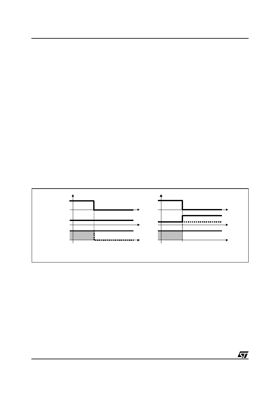
OUTPUT VOLTAGE MONITORING AND PROTECTION: POWER GOOD
The output voltage is monitored by the Slave device through the pin VSEN. If it is not within +12/-10% (typ.) of
the programmed value, the PGOOD output is forced low. PGOOD is always active in the Slave device, also dur-
ing soft-start. PGOOD in the Master device has the only masking function during soft-start. Since the master
has not the output voltage sense, it keeps the PGOOD to GND during soft-start and after this step it is freed.
The Slave device provides Over-Voltage protection: when the voltage sensed by VSEN reaches 117% (typ.) of
the reference voltage present at the VPROG_IN pin, the Slave device stops switching keeping the LS mosfets
ON. The FAULT pin is driven high (5V) and the SLAVE_OK line is pulled low. The master device then stops
switching keeping the LS mosfets ON, too. Since the condition is latched, power supply (Vcc) turn off and on is
required to restart operations.
Under voltage protection is also provided and still detected by the Slave device. If the output voltage drops be-
low the 60% (typ.) of the reference voltage present at the VPROG_IN pin for more than one clock period, the
Slave device stops switching turning OFF all mosfets and pulling down the SLAVE_OK line: the Master device
stops switching with LS mosfets ON. The OSC/INH/FAULT is not driven high in this case.
Both Over Voltage and Under Voltage are active also during soft start (Under Voltage after than Vout reaches
0.8V). During soft-start the reference voltage used to determine the UV threshold is the increasing voltage driv-
en by the 2048 soft start digital counter. Moreover, OVP is always active, even during INHIBIT (see relevant
section).
Over / Under Voltage behavior are shown in Figure 9.
Figure 9. OVP and UVP latch
REMOTE VOLTAGE SENSE
A remote sense buffer is integrated into the device to allow output voltage remote sense implementation without
any additional external components. In this way, the output voltage programmed is regulated between the re-
mote buffer inputs compensating motherboard trace losses or connector losses if the device is used for a VRM
module.
The very low offset amplifier senses the output voltage remotely through the pins FBR and FBG (FBR is for the
regulated voltage sense while FBG is for the ground sense) and reports this voltage internally at VSEN pin with
unity gain eliminating the errors. Keeping the FBR and FBG traces parallel and guarded by a power plane re-
sults in common mode coupling for any picked-up noise.
If remote sense is not required, the output voltage is sensed by the VSEN pin connecting it directly to the output
voltage. In this case the FBG and FBR pins must be connected anyway to the regulated voltage
LS
OSC
SLAVE_OK
LS
OSC
SLAVE_OK
UNDER VOLTAGE LATCH
OVER VOLTAGE LATCH
L6918
L6918A
L6918A
L6918

19/35
L6918 L6918A
INPUT CAPACITOR
The input capacitor is designed considering mainly the input rms current that depends on the duty cycle as re-
ported in figure. Considering the four phase topology, the input rms current is highly reduced comparing with
single or dual phase operation.
It can be observed that the input rms value is one half of the dual-phase equivalent input current in the worst-
case condition that happens for D=1/8, 3/8,5/8 and 7/8.
The power dissipated by the input capacitance is then equal to:
Input capacitor is designed in order to sustain the ripple relative to the maximum load duty cycle. To reach the
high rms value needed by the CPU power supply application and also to minimize components cost, the input
capacitance is realized by more than one physical capacitor. The equivalent rms current is simply the sum of
the single capacitor's rms current.
Figure 10. Input rms Current vs. Duty Cycle.
OUTPUT CAPACITOR
Since the microprocessors require a current variation beyond 100A doing load transients, with a slope in the
range of tenth A/
µ
s, the output capacitor is a basic component for the fast response of the power supply.
Dual phase topology reduces the amount of output capacitance needed because of faster load transient re-
sponse (switching frequency is doubled at the load connections). Current ripple cancellation due to the 180∞
phase shift between the two phases also reduces requirements on the output ESR to sustain a specified voltage
ripple.
When a load transient is applied to the converter's output, for first few microseconds the current to the load is
supplied by the output capacitors. The controller recognizes immediately the load transient and increases the
duty cycle, but the current slope is limited by the inductor value.
The output voltage has a first drop due to the current variation inside the capacitor (neglecting the effect of the
ESL):
P
RM S
ESR
I
R M S
(
)
2
=
0.50
0.75
0.25
0.50
0.25
Single Phase
Dual Phase
Duty Cycle (V
OUT
/V
IN
)
Rm
s
Cu
r
r
e
n
t
No
r
m
a
l
i
z
e
d
(
I
RM
S
/I
OUT
)
4 Phase
V
OU T
I
OU T
ESR
=

L6918 L6918A
20/35
A minimum capacitor value is required to sustain the current during the load transient without discharge it. The
voltage drop due to the output capacitor discharge is given by the following equation:
Where D
MAX
is the maximum duty cycle value. The lower is the ESR, the lower is the output drop during load
transient and the lower is the output voltage static ripple.
INDUCTOR DESIGN
The inductance value is defined by a compromise between the transient response time, the efficiency, the cost
and the size. The inductor has to be calculated to sustain the output and the input voltage variation to maintain
the ripple current
I
L
between 20% and 30% of the maximum output current. The inductance value can be cal-
culated with this relationship:
Where f
SW
is the switching frequency, V
IN
is the input voltage and V
OUT
is the output voltage.
Increasing the value of the inductance reduces the ripple current but, at the same time, reduces the converter
response time to a load transient. The response time is the time required by the inductor to change its current
from initial to final value. Since the inductor has not finished its charging time, the output current is supplied by
the output capacitors. Minimizing the response time can minimize the output capacitance required.
The response time to a load transient is different for the application or the removal of the load: if during the ap-
plication of the load the inductor is charged by a voltage equal to the difference between the input and the output
voltage, during the removal it is discharged only by the output voltage. The following expressions give approx-
imate response time for DI load transient in case of enough fast compensation network response:
The worst condition depends on the input voltage available and the output voltage selected. Anyway the worst
case is the response time after removal of the load with the minimum output voltage programmed and the max-
imum input voltage available.
Figure 11. Inductor ripple current vs. Vout
V
OU T
i
O U T
2
L
2 C
O U T
V
IN m in
D
M A X
V
OU T
≠
(
)
-------------------------------------------------------------------------------------------
=
L
V
IN
V
O U T
≠
f
S W
I
L
------------------------------
V
OU T
V
IN
--------------
=
t
a ppli ca tion
L
I
V
IN
V
O U T
≠
------------------------------
=
t
r em oval
L
I
V
O UT
--------------
=
Figure 12 ≠ Inductor ripple current vs. Vout
0
1
2
3
4
5
6
7
8
9
0 .5
1 .5
2 .5
3 .5
Output V oltage [V ]
Inductor Ripple [A]
L=3
µ
H,
Vin=12V
L=2
µ
H,
Vin=12V
L=1.5
µ
H, Vin=12V
L=2
µ
H,
Vin=5V
L=1.5
µ
H,
Vin=5V
L=3
µ
H, Vin=5V

21/35
L6918 L6918A
MAIN CONTROL LOOP
The four phases control loop is composed by two dual phases devices that are independent each other. So, the
compensation network and the control loop stability of each device don't depend on the other except for the fact
that the other converter represents a load for this one.
The L6918/A control loop is composed by the Current Sharing control loop and the Average Current Mode con-
trol loop. Each loop gives, with a proper gain, the correction to the PWM in order to minimize the error in its
regulation: the Current Sharing control loop equalize the currents in the inductors while the Average Current
Mode control loop fixes the output voltage equal to the reference programmed by VID. Figure 12 reports the
block diagram of the main control loop
Figure 12. Main Control Loop Diagram
CURRENT SHARING (CS) CONTROL LOOP
The devices are configured to work in a four synchronized phase application. Since the application is composed
by two-phase devices that share reference and synchronization signals, the current sharing between the phases
is realized in two different steps:
1. Sharing between the phases of the same device;
2. Sharing between devices.
The Current Sharing between phases of the same device uses the internal current information to correct the
PWM signal in order to equalize the current. Active current sharing is implemented using the information from
Tran conductance differential amplifier in an average current mode control scheme. A current reference equal
to the average of the read current (I
AVG
) is internally built; the error between the read current and this reference
is converted to a voltage with a proper gain and it is used to adjust the duty cycle whose dominant value is set
by the error amplifier at COMP pin (See fig. 13).
The current sharing control is a high bandwidth control allowing current sharing even during load transients.
The current sharing error is affected by the choice of external components; choose precise Rg resistor (±1% is
necessary) to sense the current. The current sharing error is internally dominated by the voltage mismatch of
Tran conductance differential amplifier between phases; considering a voltage mismatch equal to 2mV across
the sense resistor, the current reading error is given by the following equation:
Where
I
READ
is the difference between one phase current and the ideal current (I
MAX/2
).
For Rsense=4m
and Imax=40A the current sharing error is equal to 2.5%, neglecting errors due to Rg and
Rsense mismatches.
L1
L2
+
+
PWM1
1/5
+
-
1/5
I
INFO2
I
INFO1
4/5
Z
F(S)
PWM2
C
O
FB
COMP
R
O
ERROR
AMPLIFIER
REFERENCE
PROGRAMMED
BY VID
CURRENT
SHARING
DUTY CYCLE
CORRECTION
R
FB
D02IN1392
I
R EA D
I
M AX
--------------------
2mV
R
S EN SE
I
M AX
---------------------------------------
=

L6918 L6918A
22/35
Figure 13. Current Sharing Control Loop.
The current sharing between devices uses the droop function. Each device can be modeled with its Thevenin
equivalent circuit (that is an ideal voltage source equal to the programmed voltage by VIDs and its related output
resistance R
OUT
), while the whole converter is modeled by the same ideal voltage source and an equivalent
output resistance R
DROOP
=R
OUT
/2;
Considering this modelization reported in figure 14, it can be seen that the recirculating current between devices
depends on the accuracy of the regulation.
The accuracy of the voltage source is given by the offset of the master error amplifier Vos (6mV typ) and de-
pends on the ratio between this offset and the output voltage variation with load (R
OUT
,I
OUT
). The mismatch
between the regulated voltages causes a converter to source a current that is sunk by the other one. The accu-
racy related to droop resistance depends on precision of feedback current of the device I
FB
, sense resistors
R
SENSE
, Transconductance resistors Rg and feedback resistors R
FB
.
The current sharing error (CSE) results:
Considering the external resistors tolerance of 1%, the typical current feedback accuracy of 2.5
µ
A/50
µ
A (5%),
4 phases operation, Error Amplifier offset Vos=6mV, droop resistance R
DROOP
=1.5m
(R
OUT
=2,R
DROOP
) and
I
LOAD
=60A (I
OUT
=I
LOAD
/2), it results:
Figure 14. Equivalent Circuit for current sharing error calculation
L1
L2
+
+
PWM1
1/5
1/5
I
INFO2
I
INFO1
PWM2
COMP
V
OUT
CURRENT
SHARING
DUTY CYCLE
CORRECTION
D02IN1393
CSE
I
OU T
I
O U T
----------------
1
2
---
Vos
R
O U T
I
OU T
--------------------------------
2
1
2
---
I
FB
I
F B
------------
2
1
2
---
R
F B
R
FB
---------------
2
2
2
---
R
SEN SE
R
SE N SE
--------------------------
2
4
2
---
R
g
R
g
-----------
2
+
+
+
+
=
CSE
1
2
---
0.006V
1.5m
60A
----------------------------------
2
1
2
---
2.5
µ
A
50
µ
A
----------------
2
1
2
---
0.01
(
)
2
2
2
---
0.01
(
)
2
4
2
---
0.01
(
)
2
+
+
+
+
0.062 6.2%
(
)
=
=
VID
R
DROOP
V
OUT
R
LOAD
I
LOAD
L6
918
A
L6918
V
OUT
R
OUT
R
OUT
R
LOAD
V
PROG
Recirculating Current
I
LOAD
I
OUT
I
OUT

23/35
L6918 L6918A
AVERAGE CURRENT MODE (ACM) CONTROL LOOP
The average current mode control loop is reported in figure 15. The current information I
FB
sourced by the FB
pin flows into R
FB
implementing the dependence of the output voltage from the read current.
The ACM control loop gain results (obtained opening the loop after the COMP pin):
where:
≠
is the equivalent output resistance determined by the droop function;
≠ Z
P
(s) is the impedance resulting by the parallel of the output capacitor (and its ESR) and the applied
load Ro;
≠ Z
F
(s) is the compensation network impedance;
≠ Z
L
(s) is the parallel of the two inductor impedance;
≠ A(s) is the error amplifier gain;
≠
is the ACM PWM transfer function where
V
osc
is the oscillator ramp amplitude
and has a typical value of 2V
Removing the dependence from the Error Amplifier gain, so assuming this gain high enough, the control loop
gain results:
With further simplifications, it results:
Considering now that in the application of interest it can be assumed that Ro>>R
L
; ESR<<Ro and
R
DROOP
<<Ro, it results:
The ACM control loop gain is designed to obtain a high DC gain to minimize static error and cross the 0dB axes
with a constant -20dB/dec slope with the desired crossover frequency
T. Neglecting the effect of Z
F
(s), the
transfer function has one zero and two poles. Both the poles are fixed once the output filter is designed and the
zero is fixed by ESR and the Droop resistance.
To obtain the desired shape an R
F
-C
F
series network is considered for the Z
F
(s) implementation.
A zero at
f
=1/R
F
C
F
is then introduced together with an integrator. This integrator minimizes the static error
G
LOO P
s
( )
P WM Z
F
s
( )
R
D R O OP
Z
P
s
( )
+
(
)
Z
P
s
( )
Z
L
s
( )
+
(
)
Z
F
s
( )
A s
( )
---------------
1
1
A s
( )
------------
+
R
F B
+
--------------------------------------------------------------------------------------------------------------------
≠
=
R
DR O OP
Rsense
Rg
----------------------
R
F B
=
PWM
4
5
---
V
IN
V
OS C
-------------------
=
G
LOO P
s
( )
4
5
---
V
IN
V
OS C
-------------------
Z
F
s
( )
Z
P
s
( )
Z
L
s
( )
+
------------------------------------
Rs
Rg
--------
Z
P
s
( )
R
F B
---------------
+
≠
=
G
LOO P
s
( )
4
5
---
V
I N
V
O SC
-------------------
Z
F
s
( )
R
FB
---------------
Ro
R
D R O OP
+
Ro
R
L
2
-------
+
-------------------------------------
1
s C o
R
D R O OP
//Ro
E SR
+
(
)
+
s
2
Co
L
2
---
s
L
2 Ro
---------------
Co ESR
Co
R
L
2
-------
+
+
1
+
+
----------------------------------------------------------------------------------------------------------------------------------
≠
=
G
LOO P
s
( )
4
5
---
V
IN
V
O SC
-------------------
Z
F
s
( )
R
F B
---------------
1
s Co
R
D R O OP
ESR
+
(
)
+
s
2
Co
L
2
---
s
L
2 Ro
---------------
C o ESR
Co
R
L
2
-------
+
+
1
+
+
----------------------------------------------------------------------------------------------------------------------------------
≠
=

L6918 L6918A
24/35
while placing the zero in correspondence with the L-C resonance a simple -20dB/dec shape of the gain is as-
sured (See Figure 15). In fact, considering the usual value for the output filter, the LC resonance results to be
at frequency lower than the above reported zero.
Figure 15. ACM Control Loop Gain Block Diagram (left) and Bode Diagram (right).
Compensation network can be simply designed placing
Z
=
LC
and imposing the cross-over frequency
T
as
desired obtaining:
In a four phase operation (since the four phase converter is realized by two dual phase converters in parallel
that shares current using droop), also the other sub-system in parallel must be considered. In particular, in the
above reported relationships, it must be considered with Co and ESR the total output capacitance and equiva-
lent ESR while the output impedance Zo of the other sub-system must be considered in parallel to the output
capacitance Co and to the load Ro.
The output impedance of the other sub-system in parallel results:
Considering Zo in parallel to Ro, it can be verified that the R
F
and C
F
design relationships are still valid.
LAYOUT GUIDELINES
Since the device manages control functions and high-current drivers, layout is one of the most important things
to consider when designing such high current applications.
A good layout solution can generate a benefit in lowering power dissipation on the power paths, reducing radi-
ation and a proper connection between signal and power ground can optimize the performance of the control
loops.
Integrated power drivers reduce components count and interconnections between control functions and drivers,
reducing the board space.
Here below are listed the main points to focus on when starting a new layout and rules are suggested for a cor-
rect implementation.
dB
T
Z
LC
G
LOOP
Z
F
(s)
K
K
4
5
---
V
I N
V
osc
---------------
1
R
F B
----------
dB
=
Rout
Cout
ESR
L/2
R
FB
R
F
C
F
REF
PWM
I
FB
V
COMP
V
OUT
d
∑
V
IN
Z
F
R
F
R
F B
V
O SC
V
IN
----------------------------------
5
4
---
T
L
2
R
D R O OP
ESR
+
(
)
-------------------------------------------------------
=
C
F
Co
L
2
---
R
F
--------------------
=
Zo s
( )
Z
L
s
( )
4
5
---
V
IN
V
O SC
-------------------
Rsense
Rg
----------------------
Z
F
s
( )
+
1
4
5
---
V
IN
V
OS C
-------------------
Z
F
s
( )
R
F B
---------------
+
-----------------------------------------------------------------------------------------------
=

25/35
L6918 L6918A
Power Connections.
These are the connections where switching and continuous current flows from the input supply towards the load.
The first priority when placing components has to be reserved to this power section, minimizing the length of
each connection as much as possible.
To minimize noise and voltage spikes (EMI and losses) these interconnections must be a part of a power plane
and anyway realized by wide and thick copper traces. The critical components, i.e. the power transistors, must
be located as close as possible, together and to the controller. Considering that the "electrical" components re-
ported in figure are composed by more than one "physical" component, a ground plane or "star" grounding con-
nection is suggested to minimize effects due to multiple connections.
Fig. 16a shows the details of the power connections involved and the current loops. The input capacitance
(CIN), or at least a portion of the total capacitance needed, has to be placed close to the power section in order
to eliminate the stray inductance generated by the copper traces. Low ESR and ESL capacitors are required.
Figure 16. Power connections and related connections layout guidelines (same for both phases).
Power Connections Related.
Fig.16b shows some small signal components placement, and how and where to mix signal and power ground planes.
The distance from drivers and mosfet gates should be reduced as much as possible. Propagation delay times as
well as for the voltage spikes generated by the distributed inductance along the copper traces are so minimized.
In fact, the further the mosfet is from the device, the longer is the interconnecting gate trace and as a consequence,
the higher are the voltage spikes corresponding to the gate PWM rising and falling signals. Even if these spikes
are clamped by inherent internal diodes, propagation delays, noise and potential causes of instabilities are intro-
duced jeopardizing good system behavior. One important consequence is that the switching losses for the high
side mosfet are significantly increased.
For this reason, it is suggested to have the device oriented with the driver side towards the mosfets and the GATEx
and PHASEx traces walking together toward the high side mosfet in order to minimize distance (see fig 17). In
addition, since the PHASEx pin is the return path for the high side driver, this pin must be connected directly to
the High Side mosfet Source pin to have a proper driving for this mosfet. For the LS mosfets, the return path is the
PGND pin: it can be connected directly to the power ground plane (if implemented) or in the same way to the LS
mosfets Source pin. GATEx and PHASEx connections (and also PGND when no power ground plane is imple-
mented) must also be designed to handle current peaks in excess of 2A (30 mils wide is suggested).
V
IN
LOAD
HS
R
gate
LS
R
gate
HGATEx
PHASEx
LGATEx
PGNDx
C
IN
C
OUT
L
D
C
BOOTx
V
IN
LOAD
HS
LS
BOOTx
PHASEx
VCC
SGND
C
IN
C
OUT
L
D
+V
CC
C
V CC
a. PCB power and ground planes areas
b. PCB small signal components placement

L6918 L6918A
26/35
Figure 17. Device orientation (left) and sense nets routing (right).
Gate resistors of few ohms help in reducing the power dissipated by the IC without compromising the system
efficiency.
The placement of other components is also important:
≠ The bootstrap capacitor must be placed as close as possible to the BOOTx and PHASEx pins to min-
imize the loop that is created.
≠ Decoupling capacitor from Vcc and SGND placed as close as possible to the involved pins.
≠ Decoupling capacitor from VCCDR and PGND placed as close as possible to those pins. This capac-
itor sustains the peak currents requested by the low-side mosfet drivers.
≠ Refer to SGND all the sensible components such as frequency set-up resistor (when present) and
also the optional resistor from FB to GND used to give the positive droop effect.
≠ Connect SGND to PGND on the load side (output capacitor) to avoid undesirable load regulation ef-
fect and to ensure the right precision to the regulation when the remote sense buffer is not used.
≠ An additional 100nF ceramic capacitor is suggested to place near HS mosfet drain. This helps in re-
ducing noise.
≠ PHASE pin spikes. Since the HS mosfet switches in hard mode, heavy voltage spikes can be ob-
served on the PHASE pins. If these voltage spikes overcome the max breakdown voltage of the pin,
the device can absorb energy and it can cause damages. The voltage spikes must be limited by prop-
er layout, the use of gate resistors, Schottky diodes in parallel to the low side mosfets and/or snubber
network on the low side mosfets, to a value lower than 26V, for 20nSec, at Fosc of 600kHz max.
Current Sense Connectio ns.
≠ Remote Buffer: The input connections for this component must be routed as parallel nets from the
FBG/FBR pins to the load in order to compensate losses along the output power traces and also to
avoid the pick-up of any common mode noise. Connecting these pins in points far from the load will
cause a non-optimum load regulation, increasing output tolerance.
≠ Current Reading: The Rg resistor has to be placed as close as possible to the ISENx and PGNDSx
pins in order to limit the noise injection into the device. The PCB traces connecting these resistors to
the reading point must be routed as parallel traces in order to avoid the pick-up of any common mode
noise. It's also important to avoid any offset in the measurement and to get a better precision, to con-
nect the traces as close as possible to the sensing elements, dedicated current sense resistor or low
side mosfet R
dsON
.
≠ Moreover, when using the low side mosfet R
dsON
as current sense element, the ISENx pin is practi-
cally connected to the PHASEx pin. DO NOT CONNECT THE PINS TOGETHER AND THEN TO
THE HS SOURCE! The device won't work properly because of the noise generated by the return of
the high side driver. In this case route two separate nets: connect the PHASEx pin to the HS Source
(route together with HGATEx) with a wide net (30 mils) and the ISENx pin to the LS Drain (route to-
gether with PGNDSx). Moreover, the PGNDSx pin is always connected, through the Rg resistor, to
the PGND: DO NOT CONNECT DIRECTLY TO THE PGND! In this case the device won't work prop-
erly. Route anyway to the LS mosfet source (together with ISENx net).
Right and wrong connections are reported in Figure 18.
Symmetrical layout is also suggested to avoid any unbalance between the two phases of the converter
Towards HS mosfet
(30 mils wide)
Towards LS mosfet
(30 mils wide)
Towards HS mosfet
(30 mils wide)
To
LS
mosfet
(or sense resistor)
To
regulated
output
To
LS
mosfet
(or sense resistor)

27/35
L6918 L6918A
Figure 18. PCB layout connections for sense nets.
Interconnections between devices.
Master and Slave devices share reference and other signals for the regulation. To avoid noise injection into de-
vices, it is recommended to route these nets carefully.
≠ VPROG_IN / VPROG_OUT: This is the reference for the regulation. It must be routed far away from
any noisy trace and guarded by ground traces in order to avoid noise injection into the device. It can
be filtered with a 30nF maximum of distributed capacitance vs. signal ground.
≠ SLAVE_OK: This signal is used by the devices for the start-up synchronization and also to commu-
nicate UVP from Slave to Master device. It must be filtered by 1nF capacitor near the pin of each de-
vice to avoid the noise to cause false protection's trigger.
Demo Board Description
The L6918 demo board shows the operation of the device in a four phases application. This evaluation board al-
lows output voltage adjustability (1.100V - 1.850V) through the switches S0-S4 and high output current capability.
The board has been laid out with the possibility to use up to two D
2
PACK mosfets for the low side switch in order
to give maximum flexibility in the mosfet choice.
The four layers demo board's copper thickness is of 70
µ
m in order to minimize conduction losses considering
the high current that the circuit is able to deliver.
Demo board schematic circuit is reported in Figure 19.
Several jumpers allow setting different configurations for the device: JP3, JP4 and JP5 allow configuring the
remote buffer as desired. Simply shorting JP4 and JP5 the remote buffer is enabled and it senses the output
voltage on-board; to implement a real remote sense, leave these jumpers open and connect the FBG and FBR
connectors on the demo board to the remote load. To avoid using the remote buffer, simply short all the jumpers
JP3, JP4 and JP5. Local sense through the R7 is used for the regulation.
The input can be configured in different ways using the jumpers JP1, JP2 and JP6; these jumpers control also
the mosfet driver supply voltage. Anyway, power conversion starts from V
IN
and the device is supplied from V
CC
(See Figure 20).
NOT CORRECT
CORRECT
To
PHASE
connection
VIA to GND plane
To HS Gate
and Source
To
LS Drain
and Source
Wrong (left) and correct (right) connections for the current reading sensing nets.

L6918 L6918A
28/35
Figure 19. Demo Board Schematic
PGOOD
PGND
PGNDS2
ISEN2
LGATE2
PHASE2
UGATE2
BOOT2
VCC
SGND
OSC / INH
VID0
VID1
VID2
VID3
VID4
ISEN1
LGATE1
PHASE1
UGATE1
BOOT1
VCCDR
6
24
25
26
27
16
15
2
5
4
3
1
13
11
22
21
20
18
19
7
28
23
10
12
VPROG_OUT
SLAVE_OK
17
R25
R24
Q7
Q8
C26
L4
C32
R30
D9
C28
C11,C13,C51;
C46,C47,C52
C14..C23,
C35..C44
C24
R21
JP3
R23
S1
S0
S3
S2
S4
R26
R27
Q5
L3
Q6
C27
D10
C29
Vin
GNDin
GNDCORE
VoutCOR
PGOOD
Master
L6918A
DZ1
C31
JP2
JP1
R33
R35
R32
R34
C9,C10;
C33,C34
R38
R39
R16
Q5a
Q7a
R19
R20
JP5
JP4
FBG
PGND
PGNDS2
ISEN2
LGATE2
PHASE2
UGATE2
BOOT2
VCC
PGOOD
SYNC_OUT
SYNC/ADJ
PGNDS1
ISEN1
LGATE1
PHASE1
UGATE1
BOOT1
VCCDR
6
24
25
26
27
16
15
2
5
4
3
1
13
14
22
21
20
18
19
28
23
11
12
VPROG_IN
SLAVE_OK
SGND
OSC / INH
7
17
R4
R3
Q3
Q4
C3
L2
C7
R10
D3
C6
R2
R5
R6
Q1
L1
Q2
C4
D4
C5
FBG
FBR
Slave
L6918
C8
R13
R15
R12
R14
R18
R17
Q1a
Q3a
D5
D6
Vcc
GNDcc
FB
COMP
9
8
C48
R29
C25
R31
R28
JP6
PGNDS1
VSEN
FB
COMP
10
9
8
C1
R8
C2
R9
R7
FBR
SY
N
C
_
O
U
T
SY
N
C
_
I
N
C12
C50
C45
C49
SL/ADJ
R22
C30
C53
R11
C24
14
To Slave's
PGOOD
R37
To L6918A
Pin 6
R36
To L6918
Pin 6

29/35
L6918 L6918A
Figure 20. Power supply configuration
Two main configurations can be distinguished: Single Supply (V
CC
= V
IN
= 12V) and Double Supply (V
CC
= 12V
V
IN
= 5V or different).
≠ Single Supply: In this case JP6 has to be completely shorted. The device is supplied with the same rail
that is used for the conversion. With an additional zener diode DZ1 a lower voltage can be derived to
supply the mosfets driver if Logic level mosfet are used. In this case JP1 must be left open so that the
HS driver is supplied with V
IN
-V
DZ1
through BOOTx and JP2 must be shorted to the left to use V
IN
or to
the right to use V
IN
-V
DZ1
to supply the LS driver through VCCDR pin. Otherwise, JP1 must be shorted
and JP2 can be freely shorted in one of the two positions.
≠ Double Supply: In this case V
CC
supply directly the controller (12V) while VIN supplies the HS drains
for the power conversion. This last one can start indifferently from the 5V bus (Typ.) or from other buses
allowing maximum flexibility in the power conversion. Supply for the mosfet driver can be programmed
through the jumpers JP1, JP2 and JP6 as previously illustrated. JP6 selects now V
CC
or V
IN
depending
on the requirements.
Some examples are reported in the following Figures 21 and 22.
Figure 21. Jumpers configuration: Double Supply
Vin
GNDin
DZ1
JP2
JP1
Vcc
GNDcc
JP6
To Vcc pin
To HS Drains (Power Input)
To BOOTx (HS Driver Supply)
To VCCDR pin (LS Driver Supply)
Vin = 5V
GNDin
DZ1
JP2
JP1
Vcc = 12V
GNDcc
JP6
Vcc = 12V
HS Drains = 5V
HS Supply = 5V
VCCDR (LS Supply) = 5V
Vin = 5V
GNDin
DZ1
JP2
JP1
Vcc = 12V
GNDcc
JP6
Vcc = 12V
HS Drains = 5V
HS Supply = 12V
VCCDR (LS Supply) = 12V
(a) V
CC
= 12V; V
BOOTx
= VCCDR = V
IN
= 5V
(b) V
CC
= V
BOOTx
= VCCDR = 12V; V
IN
= 5V

L6918 L6918A
30/35
Figure 22. Jumpers configuration: Single Supply
PCB AND COMPONENT LAYOUT
Figure 23. PCB and Components Layouts (Dimensions: 10.8mm x 14.5mm)
Vin = 12V
GNDin
DZ1 6.8V
JP2
JP1
Vcc = Open
GNDcc
JP6
Vcc = 12V
HS Drains = 12V
HS Supply = 5.2V
VCCDR (LS Supply) = 12V
Vin = 12V
GNDin
DZ1
JP2
JP1
Vcc = Open
GNDcc
JP6
Vcc = 12V
HS Drains = 12V
HS Supply = 12V
VCCDR (LS Supply) = 12V
(a) V
CC
= V
IN
= VCCDR = 12V; V
BOOTx
= 5.2V
(b) V
CC
= V
IN
= V
BOOTx
= VCCDR = 12V
Component Side
Internal PGND Plane
Internal SGND Plane
Solder Side

31/35
L6918 L6918A
CPU Power Supply: 12V
IN
; 1.45V
OUT
; 110A
DC
Considering the high slope for the load transient, a high switching frequency has to be used. In addition to fast
reaction, this helps in reducing output and input capacitor. Inductance value is also reduced.
A switching frequency of 200kHz for each phase is then considered allowing large bandwidth for the compen-
sation network. Considering the high output current, power conversion will start from the 12V bus.
≠ Current Reading Network and Over Current:
Since the maximum output current is I
MAX
= 110A, the over current threshold has been set to 110A
(27.5A x 4) in the worst case (max mosfet temperature). Since the device limits the valley of the trian-
gular ripple across the inductors, the current ripple must be considered too. Considering the inductor
core saturation, a current ripple of 10A has to be considered so that the OCP threshold in worst case
becomes OCPx = 22A (27.5A-5A). Considering to sense the output current across the low-side mosfets
RdsON (two in parallel to reduce equivalent R
dsON
), each STB90NF03L has 6.5m
max at 25∞C that
becomes 9.1m
at 100∞C considering the temperature variation; the resulting transconductance resis-
tor Rg has to be:
≠ Droop function Design:
Considering a voltage drop of 85mV at full load, the feedback resistor R
FB
has to be:
≠ Inductor design:
Transient response performance needs a compromise in the inductor choice value: the biggest the in-
ductor, the highest the efficient but the worse the transient response and vice versa. Considering then
an inductor value of 1
µ
H, the current ripple becomes:
≠ Output Capacitor:
Ten Rubycon MBZ (3300
µ
F / 6.3V / 12m
max ESR) has been used implementing a resulting ESR of
1.2m
resulting in an ESR voltage drop of 52A*1.2m
= 62mV after a 52A load transient.
≠ Compensation Network:
A voltage loop bandwidth of 20kHz is considered to let the device fast react after load transient.
The R
F
C
F
network results:
(R8)
(C2)
Further adjustments can be done on the work bench to fit the requirements and to compensate layout parasitic
components.
Rg
I
O C Px
R
d sO N
35
µ
------------------
22
4.5m
35
µ
-------------
2.7 k
(R3 to R6; R24 to R27)
=
=
=
R
FB
85m V
70
µ
A
----------------
1.2 k
(R7)
=
=
I
Vin
Vo ut
≠
L
-----------------------------
d
F sw
-----------
12
1.4
≠
1
µ
---------------------
1.4
12
--------
1
200k
-------------
6.2A (L1, L2)
=
=
=
R
F
R
F B
V
O S
V
IN
------------------------------
5
4
---
T
L
2
R
D R OOP
ESR
+
(
)
-------------------------------------------------------
1.2K 2
12
--------------------
5
4
---
20k 2
1
µ
2
4.5m
2.7
-------------
1k
1.2m
+
----------------------------------------------------------
3.9k
=
=
=
C
F
C o
L
2
---
R
F
--------------------
6 3300
µ
1
µ
2
-------
3.9k
-----------------------------------------
22 nF
=
=
=

L6918 L6918A
32/35
Part List
Resistors
R2, R9, R20, R23, R31, R42
Not Mounted
SMD 0805
R3, R4, R5, R6
R24, R25, R26, R27
2.7K
1%
SMD 0805
R7, R28
1.2K
1%
SMD 0805
R11, R22
510
SMD 0805
R12 to R19
R32, R33, R34, R35, R38, R39
0
SMD 0805
R8, R29
3.9K
SMD 0805
R10, R30
82
SMD 0805
R21
10K
SMD 0805
R36, R37
1M
1%
SMD 0805
Capacitors
C1, C48
Not Mounted
SMD 0805
C2, C25
47n
SMD 0805
C24, C30
100n
SMD 0805
C3, C4, C26, C27
100n
SMD 0805
C5, C6, C7, C28, C29, C32
1
µ
SMD 0805
C8, C31
10
µ
SMD 1206
C9, C10, C33, C34
10
µ
or 22
µ
/ 16V
TDK Multilayer Ceramic
SMD 1206
C11, C13, C46, C47,
C51, C52
1800
µ
/ 16V
Rubycon MBZ
Radial 23x10.5
C12, C45, C49, C50
1n
SMD 0805
C53
1n
SMD 0805
C14, C16, C18, C20, C22
C35, C37, C39, C41, C43
3300
µ
/6.3V Rubycon MBZ
Radial 23x10.5
Diodes
D3, D4, D9, D10
1N4148
SOT23
DZ1
Not Mounted
MINIMELF
Mosfets
Q1, Q1A, Q3, Q3A,
Q5, Q5A, Q7, Q7A
STB90NF03L
STMicroelectronics
D2PACK
Q2, Q4, Q6, Q8
STB90NF03L
STMicroelectronics
D2PACK
Inductors
L1, L2, L3, L4
1
µ
77121 Core / 5 Turns 2 x 1.5 mm
Controllers
U2
L6918
STMicroelectronics
SO28

33/35
L6918 L6918A
STATIC PERFORMANCES
Figure 24 shows the demo board measured efficiency versus load current in steady state conditions without air-
flow at ambient temperature.
Figure 24. System Efficiency
Figure 25 shows the mosfets temperature versus output current in steady state condition without any air-flow
or heat sink. It can be observed that the mosfets are under 100∞C in any conditions. Load regulation is also re-
ported from 10A to 110A.
Figure 25. Mosfet Temperature and Load Regulation.
DYNAMIC PERFORMANCES
Figure 26 shows the system response to a load transient from 0A to 110A. The output voltage is contained in
the ±50mV range. Additional output capacitors can help in reducing the initial voltage spike mainly due to the
ESR.
Figure 26. 110A Load Transient Response.
55
60
65
70
75
80
85
90
0
10
20
30
40
50
60
70
80
90
100
110
Output Current [A]
Efficiency [%]
30
40
50
60
70
80
90
100
110
0
10 20
30 40 50 60
70 80 90 100 110
Output Current [A]
Temperature [
o
C]
High-Side MOS
Low-Side MOS
1.350
1.370
1.390
1.410
1.430
1.450
1.470
0
10 20 30 40 50 60 70 80 90 100 110
Output Current [A]
Vout [V]
L6918 L6918A
34/35
SO28
DIM.
mm
inch
MIN.
TYP.
MAX.
MIN.
TYP.
MAX.
A
2.65
0.104
a1
0.1
0.3
0.004
0.012
b
0.35
0.49
0.014
0.019
b1
0.23
0.32
0.009
0.013
C
0.5
0.020
c1
45
∞
(typ.)
D
17.7
18.1
0.697
0.713
E
10
10.65
0.394
0.419
e
1.27
0.050
e3
16.51
0.65
F
7.4
7.6
0.291
0.299
L
0.4
1.27
0.016
0.050
S
8
∞
(max.)
OUTLINE AND
MECHANICAL DATA

Information furnished is believed to be accurate and reliable. However, STMicroelectronics assumes no responsibility for the consequences
of use of such information nor for any infringement of patents or other rights of third parties which may result from its use. No license is granted
by implication or otherwise under any patent or patent rights of STMicroelectronics. Specifications mentioned in this publication are subject
to change without notice. This publication supersedes and replaces all information previously supplied. STMicroelectronics products are not
authorized for use as critical components in life support devices or systems without express written approval of STMicroelectronics.
The ST logo is a registered trademark of STMicroelectronics
©
2002 STMicroelectronics - All Rights Reserved
STMicroelectronics GROUP OF COMPANIES
Australia - Brazil - Canada - China - Finland - France - Germany - Hong Kong - India - Israel - Italy - Japan -Malaysia - Malta - Morocco -
Singapore - Spain - Sweden - Switzerland - United Kingdom - United States.
http://www.st.com
35/35
L6918 L6918A