 | –≠–ª–µ–∫—Ç—Ä–æ–Ω–Ω—ã–π –∫–æ–º–ø–æ–Ω–µ–Ω—Ç: L6920DC | –°–∫–∞—á–∞—Ç—å:  PDF PDF  ZIP ZIP |
June 2006
Rev 1
1/16
16
L6920DC
Synchronous rectifier step up converter
General features
0.8V start up input voltage
Up to 5.5V operating input voltage
Internal synchronous rectifier
Adjustable output voltage from 1.8V to 5.5V
3.3V and 5V fixed output voltages
Low battery voltage detection
Reverse battery protection
550mA minimum input current limit
Switching frequency up to 1MHz
1.23V reference voltage available
Applications
Conversion from 1 to 3 alkaline,
NiMH, NiCd battery cells or 1 lithium ION
PDA and handheld instruments
Digital cameras
Cellular phones
GPS
Distributed power
Description
The L6920DC is a high efficiency monolithic step
up switching converter IC especially designed for
battery powered application.
Package is MSOP8 in order to minimize PCB
space. It requires only three external components
to realize the conversion from the battery voltage
to the selected output voltage.
The minimum output voltage is 1.8V: suitable to
supply the most advanced ASIC and µP.
High switching frequency allows for a low profile,
small sized inductor and output capacitor to be
used.
Reference voltage, low battery detection and
Shutdown are provided together with over current,
over voltage.
MSOP8
www.st.com
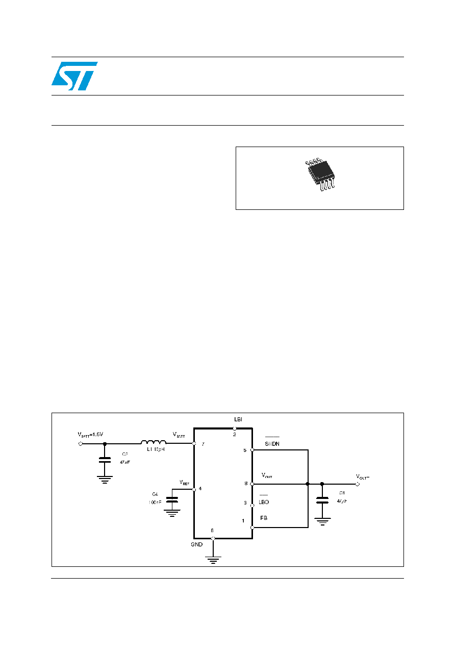
Application circuit
L6920DC
3.3V

Contents
L6920DC
2/16
Contents
1
Pin settings . . . . . . . . . . . . . . . . . . . . . . . . . . . . . . . . . . . . . . . . . . . . . . . . 3
1.1
Pin connection . . . . . . . . . . . . . . . . . . . . . . . . . . . . . . . . . . . . . . . . . . . . . . 3
1.2
Pin description . . . . . . . . . . . . . . . . . . . . . . . . . . . . . . . . . . . . . . . . . . . . . . 3
2
Electrical data . . . . . . . . . . . . . . . . . . . . . . . . . . . . . . . . . . . . . . . . . . . . . . 4
2.1
Maximum ratings . . . . . . . . . . . . . . . . . . . . . . . . . . . . . . . . . . . . . . . . . . . . 4
2.2
Thermal data . . . . . . . . . . . . . . . . . . . . . . . . . . . . . . . . . . . . . . . . . . . . . . . 4
3
Electrical characteristics . . . . . . . . . . . . . . . . . . . . . . . . . . . . . . . . . . . . . 5
4
Typical performance . . . . . . . . . . . . . . . . . . . . . . . . . . . . . . . . . . . . . . . . . 6
5
Detailed description . . . . . . . . . . . . . . . . . . . . . . . . . . . . . . . . . . . . . . . . . 7
5.1
Principle of operation . . . . . . . . . . . . . . . . . . . . . . . . . . . . . . . . . . . . . . . . . 7
5.2
Start-up . . . . . . . . . . . . . . . . . . . . . . . . . . . . . . . . . . . . . . . . . . . . . . . . . . . 9
5.3
Shutdown . . . . . . . . . . . . . . . . . . . . . . . . . . . . . . . . . . . . . . . . . . . . . . . . . 10
5.4
Low battery detection . . . . . . . . . . . . . . . . . . . . . . . . . . . . . . . . . . . . . . . . 10
5.5
Low battery input . . . . . . . . . . . . . . . . . . . . . . . . . . . . . . . . . . . . . . . . . . . 10
5.6
Reverse polarity . . . . . . . . . . . . . . . . . . . . . . . . . . . . . . . . . . . . . . . . . . . . 10
5.7
Output voltage selection . . . . . . . . . . . . . . . . . . . . . . . . . . . . . . . . . . . . . . 10
6
Package mechanical data . . . . . . . . . . . . . . . . . . . . . . . . . . . . . . . . . . . . 12
7
Order code . . . . . . . . . . . . . . . . . . . . . . . . . . . . . . . . . . . . . . . . . . . . . . . . 14
8
Revision history . . . . . . . . . . . . . . . . . . . . . . . . . . . . . . . . . . . . . . . . . . . 15
L6920DC
Pin settings
3/16
1 Pin
settings
1.1 Pin
connection
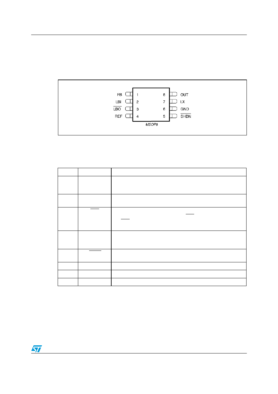
Figure 1.
Pin connection (top view)
1.2 Pin
description
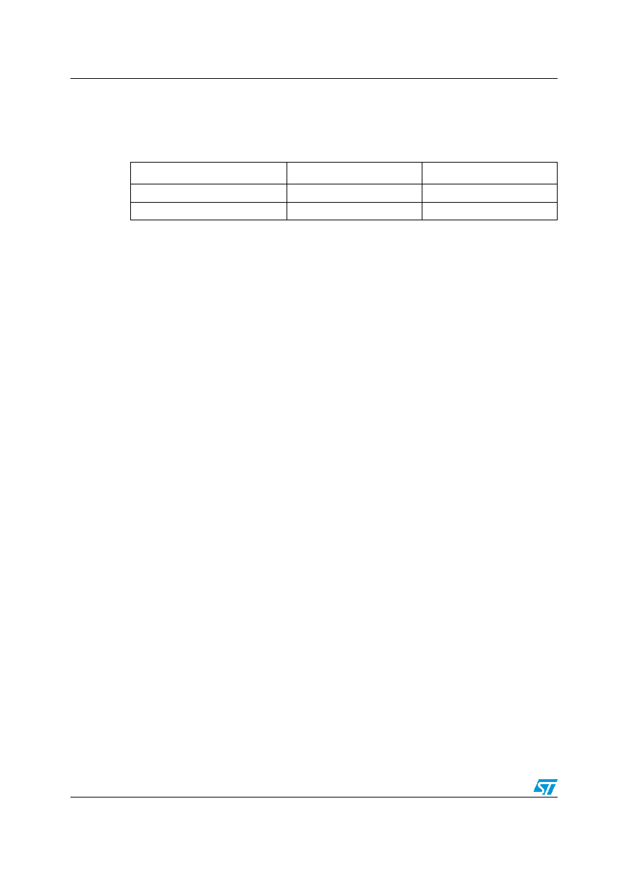
Table 1. Pin description
N∞
Type
Description
1
FB
Output voltage selector. Connect FB to GND for Vout=5V or to OUT for
Vout=3.3V. Connect FB to an external resistor divider for adjustable
output voltage
2
LBI
Battery low voltage detector input. The internal threshold is set to 1.23V.
A resistor divider is needed to adjust the desired low battery threshold.
3
LBO
Battery low voltage detector output. If the voltage at the LBI pin drops
below the internal threshold typ. 1.23V, LBO goes low.
The
LBO
is an open drain output and so a pull-up resistor (about
200K
) has to be added for correct output setting .
4
REF
1.23V reference voltage. Bypass this output to GND with a 100nF
capacitor for filtering high frequency noise. No capacitor is required for
stability
5
SHDN
Shutdown pin. When pin 5 is below 0.2V the device is in shutdown,
when pin 5 is above 0.6V the device is operating.
6
GND
Ground pin
7
LX
Step-up inductor connection
8
OUT
Power OUTPUT pin
Electrical data
L6920DC
4/16
2 Electrical
data
2.1 Maximum
ratings
2.2 Thermal
data
Table 2. Absolute maximum ratings
Symbol
Parameter
Value
Unit
V
ccmax
V
cc
to GND
6
V
LBI, SHDN, FB to GND
6
V
V
out max
Vout to GND
6
V
Table 3. Thermal data
Symbol
Parameter
Value
Unit
R
thJA
Maximum thermal resistance junction-ambient
180
∞ C/W
T
J
Maximum junction temperature
150
∞ C

L6920DC
Electrical characteristics
5/16
3 Electrical
characteristics
Table 4. Electrical characteristcs
(V
IN
= 2V, FB = GND, T
J
= 25∞C unless otherwise specified)
Symbol
Parameter
Test condition
Min
Typ
Max
Unit
V
CC
Section
V
IN
Minimum Start Up Input
Voltage
V
out
= 3.3V
0.8
V
I
q
Quiescent Current
I
l
= 0 mA, FB = 1.4V, V
out
= 3.3V
LBI = SHDN = 2V
9
12
µA
I
l
= 0 mA, FB = 1.4V, V
out
= 5V
LBI = SHDN = 2V
11
15
µA
I
sd
Shut Down Current
V
in
= 5V, I
l
= 0 mA
0.1
1
µA
Irev
Reverse battery current
V
in
= -4V
0.1
1
µA
Power section
R
on-N
Active switch ON resistance
300
m
R
on-P
Synchronous switch ON
resistance
300
m
Control section
V
out
Output voltage
FB = OUT, I
l
= 0 mA
3.2
3.3
3.4
V
FB = GND, I
l
= 0 mA
4.9
5
5.1
V
Output voltage range
External divider
1.8
5.5
V
V
LBI
LBI threshold
1.23
V
V
LBO
LBO
logic LOW
I
sink
= 1mA
0.2
0.4
V
I
lim
LX switch current limit
0.55
0.9
A
T
onmax
Maximum on time
V
out
= 3.3V
3.75
5
6.25
µs
T
offmin
Minimum off time
V
out
= 3.3V
0.75
1
1.25
µs
SHDN
SHDN
logic LOW
0.2
V
SHDN
logic HIGH
0.6
V
V
ref
Reference Voltage
1.18
1.23
1.27
V

Typical performance
L6920DC
6/16
4 Typical
performance
Figure 2.
Efficiency vs output current @ V
OUT
= 3.3V
Figure 3.
Efficiency vs output current @ V
OUT
= 5V
Figure 4.
Start up voltage vs output current @ V
out
= 5V & V
out
= 3.3V
40
45
50
55
60
65
70
75
80
85
90
95
0.1
1
10
100
1000
Vin=2.4V
Vin=1.2V
L6920DB
Vout=3.3V
L=10µH
Cout=47µF
Cin=10µF
L6920DC
0
10
20
30
40
50
60
70
80
90
100
0.1
1
10
100
1000
Vin=3.6V
Vin=2.4V
Vin=1.2V
L6920DB
Vout=5V
L=10µH
Cout=47µF
Cin=10µF
L6920DC
VStart up vs . out put cur rent
600
700
800
900
1000
1100
1200
1300
1400
1500
1600
0.1
1
10
100
1000
Out put cu rrent (mA)
VSt
a
r
t
u
p
(
m
V)
VStart up v s. output current
600
700
800
900
1000
1100
1200
1300
1400
1500
1600
0.1
1
10
100
1000
Output current (mA)
V
S
ta
r
t
u
p
(mV
)
Vout =3.3V
Vout =5V
L6920DC
Detailed description
7/16
5 Detailed
description
The L6920DC is a high efficiency, low voltage step-up DC/DC converter particularly suitable
for 1 to 3 cells (Li-Ion/ polymer, NiMH respectively) battery up conversion.
These performances are achieved via a strong reduction of quiescent current (10
µA only)
and adopting a synchronous rectification that implies also a reduced cost in the application
(no external diode required).
Operation is based on maximum ON time - minimum OFF time control.
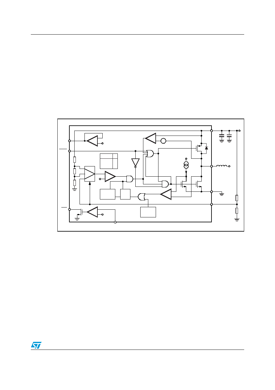
A simplified block diagram is shown here below.
Figure 5.
Simplified block diagram
5.1
Principle of operation
In L6920DC the control is based on a comparator that continuously checks the status of
output voltage.
If the output voltage is lower than the expected value, the control function of the L6920DC
directs the energy stored in the inductor to be transferred to the load. This is accomplished
by alternating between two basic steps:
T
ON
phase: the energy is transferred from the battery to the inductor by shorting LX
node to ground via the N-channel power switch. The switch is turned off if the current
flowing in the inductor reaches the current limit or after a maximum on time set to 5
µs.
T
OFF
phase: the energy stored in the inductor is transferred to the load through the
synchronous switch for at least a minimum off time equal to 1
µs. After this, the
synchronous switch is turned off as soon as the output voltage goes lower than the
regulated voltage or the current flowing in the inductor goes down to zero.
R
Q
S
Ton max
5
µsec
Toff min
1
µsec
VBG
VBG
VBG
A
B
C
-
+
-
+
-
+
-
+
-
+
VOUT
ZERO CROSSING
OPAMP
(CR)
CURRENT LIMIT
OUT
FB
GND
V
REF
LBI
LBO
D99IN1041
SHDN
LX
V
IN
V
OUT
V
OUT
GND
R
1
,R
2
FB
Y
Y
A
B
C
- +
Detailed description
L6920DC
8/16
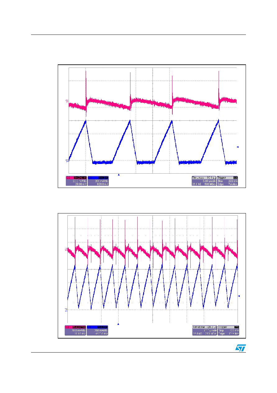
So, in case of light load, the device works in PFM mode, as shown in
Figure 8
:
Figure 6.
PFM mode condition: V
out
= 5V; V
batt
=1.5V ; C2 = V
out
; C3 = Inductor
Current
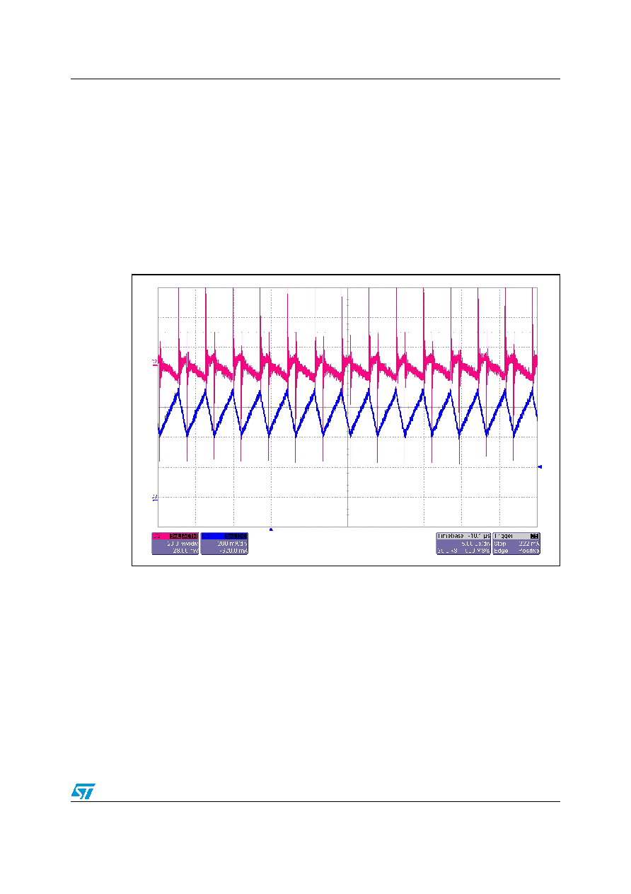
Figure 7
shows how the device works in case of heavy load.
Figure 7.
Heavy load conditions C2 = V
out
; C3 = Inductor Current; V
out
= 5V;
V
batt
=1.5V
L6920DC
Detailed description
9/16
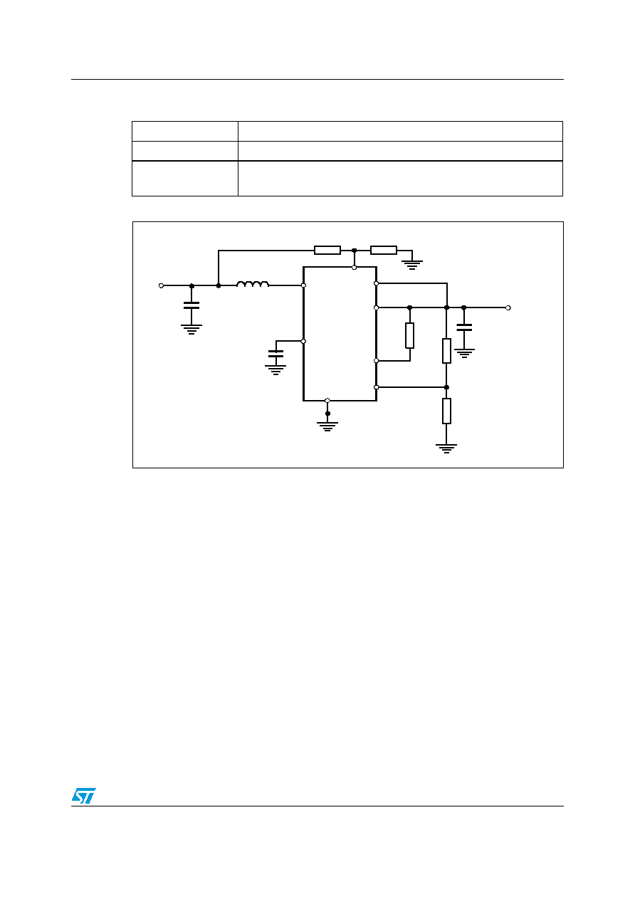
The maximum load current is defined by the following relationship:
Equation 1
Where
is the efficiency and I
LIM
is the current limit.
Of course, if I
LOAD
is greater than I
LOAD_LIM
the regulation is lost (
Figure 8
).
Figure 8.
No regulation C2 = V
out
; C3 = Inductor Current
5.2 Start-up
One of the key features of L6920DC is the startup at supply voltage down to 0.8V (please
see the diagram in
Figure 4
).
The device leaves the startup mode of operation as soon as Vout goes over 1.4V. During
startup, the synchronous switch is off and the energy is transferred to the load through its
intrinsic body diode.
The N-channel switches with a very low R
DS(on)
thanks to an internal charge pump used to
bias the power MOS gate. Because of this modified behavior, T
ON
/T
OFF
times are
lengthened. Current limit and zero crossing detection are still available.
I
LOAD_LIM
V
in
V
out
-----------
I
LIM
T
OFF_MIN
V
out
V
in
≠
2
L
-------------------------
≠
=

Detailed description
L6920DC
10/16
5.3 Shutdown
In shutdown mode (SHDN pulled low) all internal circuitries are turned off, minimizing the
current provided by the battery (I
SHDN
< 100 nA, in typical case).
Both switches are turned off, and the low battery comparator output is forced in high
impedance state.
The synchronous switch body diode causes a parasitic path between power supply and
output that can't be avoided also in shutdown.
5.4
Low battery detection
The L6920DC includes a low battery detector comparator.
Threshold is V
REF
voltage and a hysteresis is added to avoid oscillations when input crosses
the threshold slowly. The LBO is an open drain output so a pull up resistor is required for a
proper use.
5.5
Low battery input
It is possible to fix, using an external resistor divider, the LBO threshold, in order to adapt
the LBO detection at the correct input source, by the following equation:
Equation 2
Where V
batt-th
is the battery voltage at which the internal comparetor is triggered.
5.6 Reverse
polarity
A protection circuit has been implemented to avoid that L6920DC and the battery are
destroyed in case of wrong battery insertion.
In addition, this circuit has been designed so that the current required by the battery is zero
also in reverse polarity.
If a battery can be inserted in reverse direction, a non polarized capacitor should be
installed in location of C2.
5.7
Output voltage selection
Output voltage must be selected acting on FB pin.
Three choices are available: fixed 3.3V, 5V or adjustable output set via an external resistor
divider.
V
batt-th
1.23V
=
1
R1
R2
--------
+
L6920DC
Detailed description
11/16
Figure 9.
Test circuit
Table 5. Output voltage connection
V
out
= 3.3V
FB pin connected to OUT (see application circuit)
V
out
= 5V
FB pin connected to GND
1.8V < V
out
< 5.5V
FB pin connected to a resistive divider V
out
1.23V
1
R4
R5
--------
+
=
V
BATT
LBI
V
OUT
V
REF
GND
___
LBO
_____
SHDN
FB
1
2
3
4
5
6
7
8
L6920DB
V
BATT
=1.5V
V
OUT
=2.5V
C4
100nF
C1
47
µF
C2
47
µF
L1 10
µH
R4
200K
R5
200K
R3
R1
R2
V
BATT
LBI
V
OUT
V
REF
GND
___
LBO
_____
SHDN
FB
1
2
3
4
5
6
7
8
L6920DB
V
BATT
=1.5V
V
OUT
=2.5V
C4
100nF
C1
47
µF
C2
47
µF
L1 10
µH
R4
200K
R5
200K
R3
R1
R2
L6920DC

Package mechanical data
L6920DC
12/16
6
Package mechanical data
In order to meet environmental requirements, ST offers these devices in ECOPACKÆ
packages. These packages have a Lead-free second level interconnect . The category of
second level interconnect is marked on the package and on the inner box label, in
compliance with JEDEC Standard JESD97. The maximum ratings related to soldering
conditions are also marked on the inner box label. ECOPACK is an ST trademark.
ECOPACK specifications are available at:
www.st.com
L6920DC
Package mechanical data
13/16
Table 6. MSOP8 Mechanical data
Dim.
mm.
inch
Min
Typ
Max
Min
Typ
Max
A 1.10
0.043
A1 0.050
0.150
0.002
0.006
A2 0.750
0.850
0.950 0.03 0.033
0.037
b 0.250
0.400
0.010
0.016
c 0.130
0.230
0.005
0.009
D
(1)
1.
D and F does not include mold flash or protrusions. Mold flash or potrusions shall not exceed 0.15mm
(.006inch) per side.
2.900 3.000 3.100 0.114 0.118 0.122
E 4.650 4.900 5.150 0.183 0.193 0.20
E1
(1)
2.900 3.000 3.100 0.114 0.118 0.122
e 0.650
0.026
L
0.400 0.550 0.700 0.016 0.022 0.028
L1 0.950
0.037
k
0∞ (min.) 6∞ (max.)
aaa 0.100
0.004
Figure 10. Package dimensions
Order code
L6920DC
14/16
7 Order
code
Table 7. Order code
Part number
Package
Packaging
L6920DC
MSOP8
Tube
L6920DCTR
MSOP8
Tape and reel

L6920DC
Revision history
15/16
8 Revision
history
Table 8. Revision history
Date
Revision
Changes
29-Jun-2006
1
First issue

L6920DC
16/16
Please Read Carefully:
Information in this document is provided solely in connection with ST products. STMicroelectronics NV and its subsidiaries ("ST") reserve the
right to make changes, corrections, modifications or improvements, to this document, and the products and services described herein at any
time, without notice.
All ST products are sold pursuant to ST's terms and conditions of sale.
Purchasers are solely responsible for the choice, selection and use of the ST products and services described herein, and ST assumes no
liability whatsoever relating to the choice, selection or use of the ST products and services described herein.
No license, express or implied, by estoppel or otherwise, to any intellectual property rights is granted under this document. If any part of this
document refers to any third party products or services it shall not be deemed a license grant by ST for the use of such third party products
or services, or any intellectual property contained therein or considered as a warranty covering the use in any manner whatsoever of such
third party products or services or any intellectual property contained therein.
UNLESS OTHERWISE SET FORTH IN ST'S TERMS AND CONDITIONS OF SALE ST DISCLAIMS ANY EXPRESS OR IMPLIED
WARRANTY WITH RESPECT TO THE USE AND/OR SALE OF ST PRODUCTS INCLUDING WITHOUT LIMITATION IMPLIED
WARRANTIES OF MERCHANTABILITY, FITNESS FOR A PARTICULAR PURPOSE (AND THEIR EQUIVALENTS UNDER THE LAWS
OF ANY JURISDICTION), OR INFRINGEMENT OF ANY PATENT, COPYRIGHT OR OTHER INTELLECTUAL PROPERTY RIGHT.
UNLESS EXPRESSLY APPROVED IN WRITING BY AN AUTHORIZE REPRESENTATIVE OF ST, ST PRODUCTS ARE NOT DESIGNED,
AUTHORIZED OR WARRANTED FOR USE IN MILITARY, AIR CRAFT, SPACE, LIFE SAVING, OR LIFE SUSTAINING APPLICATIONS,
NOR IN PRODUCTS OR SYSTEMS, WHERE FAILURE OR MALFUNCTION MAY RESULT IN PERSONAL INJURY, DEATH, OR
SEVERE PROPERTY OR ENVIRONMENTAL DAMAGE.
Resale of ST products with provisions different from the statements and/or technical features set forth in this document shall immediately void
any warranty granted by ST for the ST product or service described herein and shall not create or extend in any manner whatsoever, any
liability of ST.
ST and the ST logo are trademarks or registered trademarks of ST in various countries.
Information in this document supersedes and replaces all information previously supplied.
The ST logo is a registered trademark of STMicroelectronics. All other names are the property of their respective owners.
© 2006 STMicroelectronics - All rights reserved
STMicroelectronics group of companies
Australia - Belgium - Brazil - Canada - China - Czech Republic - Finland - France - Germany - Hong Kong - India - Israel - Italy - Japan -
Malaysia - Malta - Morocco - Singapore - Spain - Sweden - Switzerland - United Kingdom - United States of America
www.st.com