1/46
L7250
July 2001
This is preliminary information on a new product now in development. Details are subject to change without notice.
s
12V & 5V (±10%) OPERATION
s
REGISTER BASED ARCHITECTURE
s
3 WIRE SERIAL COMMUNICATION
INTERFACE UP TO 33 MHZ
s
BCD TECHNOLOGY
Spindle Motor Controller
s
INTERNAL POWER DEVICE 0.9 OHM MAX
VALUE @ 125∞C (SINK+SOURCE)
s
2.5A PEAK CURRENT CAPABILITY
s
ST SMOOTHDRIVE SINUSOIDAL PWM
COMMUTATION
s
DEDICATED ADC FOR POWER SUPPLY
VOLTAGE COMPENSATION
s
SPINDLE CURRENT LIMITING VIA FIXED
FREQUENCY PWM OF SPINDLE POWER
OUTPUTS AT THE SMOOTHDRIVE PWM
RATE
s
SYNCHRONOUS RECTIFICATION DURING
PWM TO REDUCE POWER DISSIPATION
s
CURRENT SENSING VIA EXTERNAL
CURRENT SENSE RESISTOR
s
INDUCTIVE SENSE POSITION START UP
DRIVEN BY
µ
PROCESSOR
s
SPINDLE BRAKING DURING POWER DOWN
CONDITION
Voice Coil Motor Driver with Ramp Load/Unload
s
INTERNAL POWER DEVICE 0.9 OHM MAX
VALUE @ 125∞C (SINK+SOURCE)
s
2A PEAK CURRENT CAPABILITY
s
15 BIT LINEAR DAC FOR CURRENT
COMMAND, WITH INTERNAL REFERENCE
VOLTAGE
s
SENSE AMPLIFIER GAIN SWITCH
s
CLASS AB OUTPUT STAGE WITH ZERO
DEAD-BAND AND MINIMAL CROSSOVER
DISTORTION
s
RAMP LOAD AND UNLOAD CAPABILITY AS
WELL AS CONSTANT VOLTAGE RETRACT
s
EXTERNAL CURRENT SENSE RESISTOR IN
SERIES WITH MOTOR.
s
HIGH CMRR (>70DB) AND PSRR (>60DB)
SENSE AMP
s
EXTERNAL CURRENT CONTROL LOOP
COMPENSATION
s
HIGH BANDWIDTH VCM CURRENT
CONTROL LOOP CAPABILITY
s
HIGH PSRR, LOW OFFSET, LOW DRIFT GM
LOOP
s
VCM VOLTAGE MODE, CONTROLLED BY
VCM DAC
s
GM LOOP OFFSET CALIBRATION SCHEME
INCLUDES A COMPARATOR ON THE
ERROR AMP
Auxiliary Functions
s
3.3V AND 1.8V LINEAR REGULATOR
CONTROLLER
s
NEGATIVE VOLTAGE REGULATOR
s
INTERNAL ISOFET 0.1 OHM @125C
s
POWER MONITOR OF 12V, 5V, 3.3V AND
1.8V
s
SHOCK SENSOR CIRCUIT TAKES INPUTS
FROM PIEZO OR CHARGING ELEMENT
s
10 BIT ADC WITH 4 MUXED INPUTS
s
THERMAL SENSE CIRCUIT AND OVER
TEMPERATURE SHUT DOWN
s
CHARGE PUMP BOOST VOLTAGE
GENERATOR FOR HIGH SIDE GATE DRIVE
s
ANALOG PINS AVAILABLE TO ENTER
SIGNALS TO BE CONVERTED BY THE
INTERNAL ADC
DESCRIPTION
L7250 is a power IC for driving the SPINDLE and
VCM motors, suitable for 5V & 12V application. The
spindle system includes integrated power FETs
which are driven using ST's Smoothdrive pseudo-si-
nusoidal commutation technology. The voice coil mo-
tor (VCM) system includes integrated power FETs,
as well as ramp load and unload capability. Linear
3.3V and1.8V voltage regulators are included, as well
as a negative regulator.
Power monitoring of VCC5, VCC12, and of the two
positive voltage regulators is also included.L7250
uses a 3 wire serial interface: S_DATA, S_CLK and
S_ENABLE
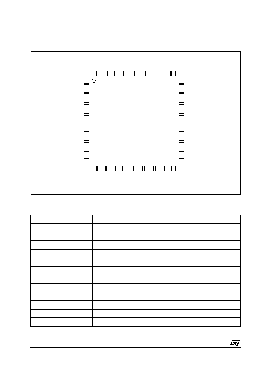
TQFP64
ORDERING NUMBER: L7250
PRODUCT PREVIEW
5V & 12V SPINDLE AND VCM MOTORS DRIVER

3/46
L7250
13
25_BASE
O5
Reg 1.8V ext NPN base
14
25_FEED
I5
Reg 1.8V feedback
15
33_BASE
O5
Reg 3.3V ext NPN base
16
33_FEED
IO5
Reg 3.3 V feedback
17
CPOR
IO5
POR delay capacitor
18
NPOR
O5
POR output signal
19
CBRAKE
IO5
Spindle brake capacitor
20
AGND
gnd
analog gnd
21
VREF25
IO5
2.5V reference
22
ZC
O5
Spindle zero crossing
23
Skin
I5
Shock sensor input
24
Skout
O5
Shock sensor 1st opamp output
25
SkFin
I5
Shock sensor filter input
26
SkFout
O5
Shock sensor filter output
27
SkDout
O5
Shock sensor output
28
Timer1
IO5
Timer 1 for unload procedure
29
CalCoarse
I5
VCM BEMF coarse calibration
30
ADaux
I5
auxiliary input for the ADC
31
VCMBEMF
O5
VCM BEMF processor output
32
Test
IO5
used for testing porpouse (*)
33
SEN
I5
Serial enable
34
SDATA
IO5
Serial data
35
SYSClk
I5
System clock
36
SCLK
I5
Serial clock
37
DAC_OUT
O5
VCM DAC output
38
ERR_IN
I5
VCM error opamp input
39
ERR_OUT
O5
VCM error opamp output
40
SNS_OUT
O5
VCM sense opamp output
41
SNS_P
I12
VCM sense opamp positive input
42
SNS_N
I12
VCM sense opamp negative input
43
VCMGND3
gnd
VCM power ground
PIN DESCRIPTION (continued)
N∞
Pin
V
Description

L7250
4/46
(*) used also to set the IC power supply application. If this pin is pull-up externally the L7250 became a 5V application
S = Supply ; IO = Input/Output ; I = Input ; O = Output ; gnd = Ground.
44
VCMGND4
gnd
VCM power ground
45
VCMN1
O12
VCM negative output
46
VCMN2
O12
VCM negative output
47
RSEN1
O12
Spindle power sensing resitor
48
RSEN2
O12
Spindle power sensing resitor
49
Rsense
I5
Spindle sensing resistor input
50
OUTW1
O12
Spindle phase C output
51
OUTW2
O12
Spindle phase C output
52
VM1
IO12
Vmotor
53
VM2
IO12
Vmotor
54
VCV4
S12
12V power supply
55
VCV3
S12
12V power supply
56
OUTV1
O12
Spindle phase B output
57
OUTV2
O12
Spindle phase B output
58
RSEN3
O12
Spindle power sensing resitor
59
RSEN4
O12
Spindle power sensing resitor
60
OUTU1
O12
Spindle phase A output
61
OUTU2
O12
Spindle phase A output
62
CT
I12
Spindle central tap
63
CPOSCH
IO20
Charge pump diodes connection
64
VBOOST
IO20
Charge Pump voltage
PIN DESCRIPTION (continued)
N∞
Pin
V
Description

5/46
L7250
ELECTRICAL CHARACTERISTCS
ABSOLUTE MAXIMUM RATINGS
Symbol
Parameter
Value
Unit
VCV1,VCV2,VCV3,VCV4
14
V
VCC5 maximum voltage
6
V
OUTU1,OUTU2,OUTV1,OUTV2,OUTW1,OUTW2
VCMP1,VCMP2,VCMN1,VCMN2
VM1,VM2
-1V to 16
V
Digital Input Voltage
-0.3 to VCC5
V
Operating free-air temperature
0 to 70
∞C
Storage Temperature
-55 to 150
∞C
ELECTRICAL CHARACTERISTCS
POWER SUPPLY [VCC5 & VCV] VCC5 = 5V ±10%, VCV = 12V ±10%. T
amb
= 25∞C (unless otherwise specified)
Symbol
Parameter
Test Condition
Min.
Typ.
Max.
Unit
POWER MONITOR, SUPPLY CURRENTS, ETC.
Icc5
VCC5 Operating current
Spindle and VCM enabled, no
load
9
mA
Ivcv
VCV + VRET Operating current
Spindle and VCM enabled, no
load
44
mA
CHARGE PUMP VOLTAGE BOOSTER
VBOOS
T
Charge pump output voltage
VCV = 12V
Iload = 5mA
18.5
V
VBOOS
Tfreq
Switching frequency
1
MHz
POWER MONITOR
vt5
VCC5 threshold
4.0
4.175
4.35
V
vt12
VCC12 threshold
9
9.5
10
V
hv5
VCC5 hysteresis
40
100
160
mV
hv12
VCC12 hysteresis
100
200
300
mV
vt33
V33 Threshold
2.7
2.8
2.9
V
hv33
V33 Hysteresis
20
40
60
mV
vt18
V18 Threshold (at pin 25_FEED)
1.07
1.12
1.17
V
hv18
V18Hysteresis
25
50
75
mV
NPOR
low
NPOR low level output voltage
VCV > 4.5V Iol = 5mA
0.75
V