 | –≠–ª–µ–∫—Ç—Ä–æ–Ω–Ω—ã–π –∫–æ–º–ø–æ–Ω–µ–Ω—Ç: L78M08C | –°–∫–∞—á–∞—Ç—å:  PDF PDF  ZIP ZIP |
1/21
October 2003
s
OUTPUT CURRENT TO 0.5A
s
OUTPUT VOLTAGES OF 5; 6; 8; 9; 12; 15;
18; 20; 24V
s
THERMAL OVERLOAD PROTECTION
s
SHORT CIRCUIT PROTECTION
s
OUTPUT TRANSITION SOA PROTECTION
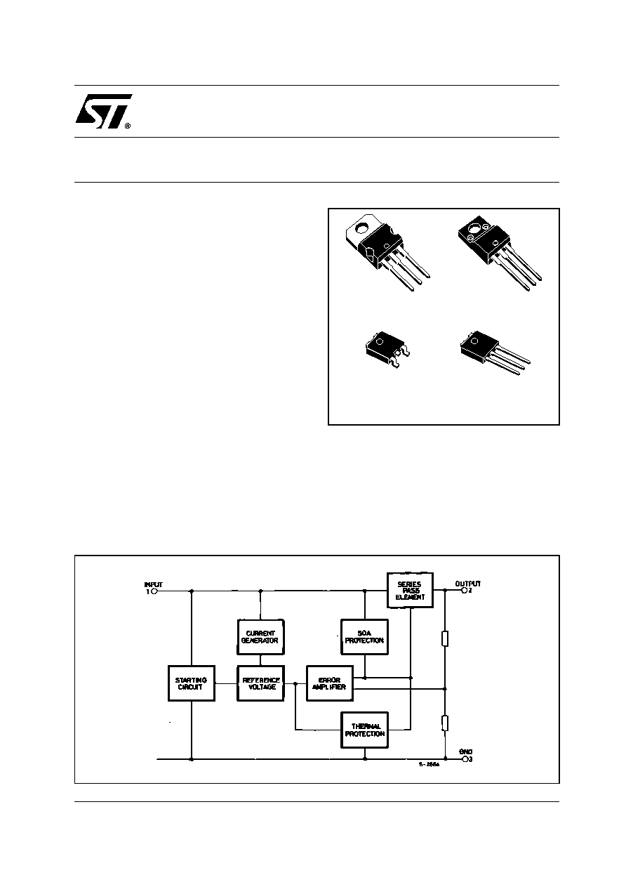
DESCRIPTION
The L78M00 series of three-terminal positive
regulators is available in TO-220, TO-220FP,
DPAK and IPAK packages and with several fixed
output voltages, making it useful in a wide range of
applications. These regulators can provide local
on-card regulation, eliminating the distribution
problems associated with single point regulation.
Each type employs internal current limiting,
thermal shut-down and safe area protection,
making it essentially indestructible. If adequate
heat sinking is provided, they can deliver over
0.5A output current. Although designed primarily
as fixed voltage regulators, these devices can be
used
with
external
components
to
obtain
adjustable voltage and currents.
L78M00
SERIES
POSITIVE VOLTAGE REGULATORS
SCHEMATIC DIAGRAM
TO-220
DPAK
TO-220FP
IPAK
L78M00 SERIES
2/21
ABSOLUTE MAXIMUM RATINGS
Absolute Maximum Ratings are those values beyond which damage to the device may occur. Functional operation under these condition is
not implied.
THERMAL DATA
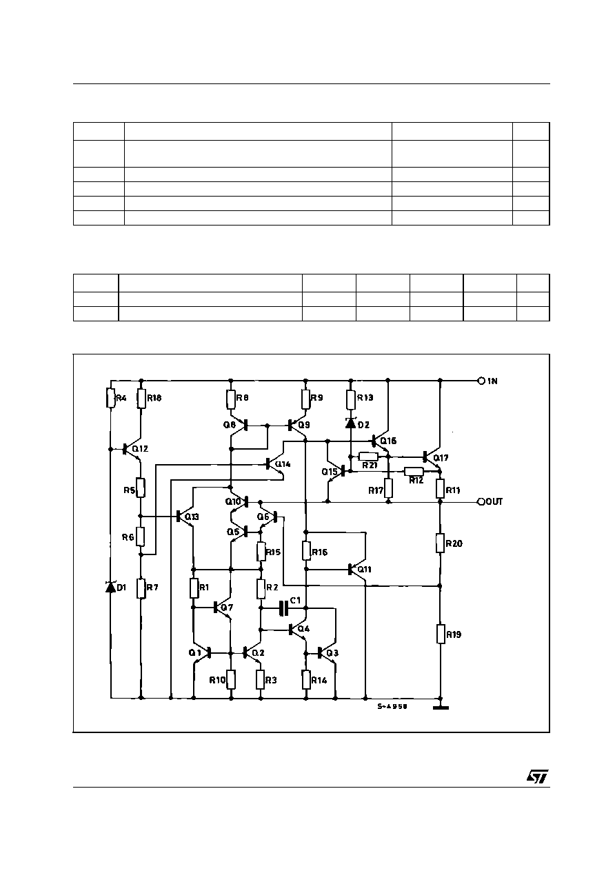
SHEMATIC DIAGRAM
Symbol
Parameter≤
Value
Unit
V
I
DC Input Voltage
(for V
O
= 5 to 18V)
(for V
O
= 20, 24V)
35
40
V
V
I
O
Output Current
Internally Limited
mA
P
D
Power Dissipation
Internally Limited
mW
T
stg
Storage Temperature Range
-65 to +150
∞C
T
op
Operating Junction Temperature Range
0 to +150
∞C
Symbol
Parameter
TO-220
TO-220FP
DPAK
IPAK
Unit
R
thj-case
Thermal Resistance Junction-case
3
5
8
∞C/W
R
thj-amb
Thermal Resistance Junction-ambient
50
60
100
∞C/W

L78M00 SERIES
3/21
CONNECTION DIAGRAM (top view)
ORDERING CODES
(*) Available in Tape & Reel with the suffix "-TR".
APPLICATION CIRCUITS
TYPE
TO-220
TO-220FP
DPAK (*)
IPAK
OUTPUT
VOLTAGE
L78M05
L78M05CV
L78M05CP
L78M05CDT
L78M05CDT-1
5 V
L78M06
L78M06CV
L78M06CP
L78M06CDT
L78M06CDT-1
6 V
L78M08
L78M08CV
L78M08CP
L78M08CDT
L78M08CDT-1
8 V
L78M09
L78M09CV
L78M09CP
L78M09CDT
L78M09CDT-1
9 V
L78M10
L78M10CV
L78M10CP
L78M10CDT
L78M10CDT-1
10 V
L78M12
L78M12CV
L78M12CP
L78M12CDT
L78M12CDT-1
12 V
L78M15
L78M15CV
L78M15CP
L78M15CDT
L78M15CDT-1
15 V
L78M18
L78M18CV
L78M18CP
L78M18CDT
L78M18CDT-1
18 V
L78M20
L78M20CV
L78M20CP
L78M20CDT
L78M20CDT-1
20 V
L78M24
L78M24CV
L78M24CP
L78M24CDT
L78M24CDT-1
24 V
TO-220
TO-220FP
IPAK
DPAK
L78M00 SERIES
4/21
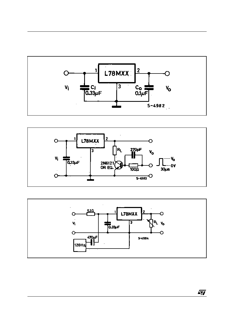
TEST CIRCUITS
Figure 1 : DC Parameter
Figure 2 : Load Regulation
Figure 3 : Ripple Rejection
L78M00 SERIES
5/21
ELECTRICAL CHARACTERISTICS OF L78M05C (refer to the test circuits, T
J
= 25∞C, V
I
= 10V,
I
O
= 350 mA, C
I
= 0.33 µF, C
O
= 0.1 µF unless otherwise specified).
ELECTRICAL CHARACTERISTICS OF L78M06C (refer to the test circuits, T
J
= 25∞C, V
I
= 11V,
I
O
= 350 mA, C
I
= 0.33 µF, C
O
= 0.1 µF unless otherwise specified).
Symbol
Parameter
Test Conditions
Min.
Typ.
Max.
Unit
V
O
Output Voltage
4.8
5
5.2
V
V
O
Output Voltage
I
O
= 5 to 350 mA
V
I
= 7 to 20 V
4.75
5
5.25
V
V
O
Line Regulation
V
I
= 7 to 25 V
I
O
= 200 mA
100
mV
V
I
= 8 to 25 V
I
O
= 200 mA
50
V
O
Load Regulation
I
O
= 5 to 500 mA
T
J
= 25∞C
100
mV
I
O
= 5 to 200 mA
T
J
= 25∞C
50
I
d
Quiescent Current
6
mA
I
d
Quiescent Current Change
I
O
= 5 to 350 mA
0.5
mA
I
O
= 200 mA
V
I
= 8 to 25 V
0.8
V
O
/
T Output Voltage Drift
I
O
= 5 mA
T
J
= 0 to 125∞C
-0.5
mV/∞C
SVR
Supply Voltage Rejection
V
I
= 8 to 18 V
f = 120Hz
I
O
= 300mA
62
dB
eN
Output Noise Voltage
B =10Hz to 100KHz
40
µ
V
V
d
Dropout Voltage
2
V
I
sc
Short Circuit Current
V
I
= 35 V
300
mA
Symbol
Parameter
Test Conditions
Min.
Typ.
Max.
Unit
V
O
Output Voltage
5.75
6
6.25
V
V
O
Output Voltage
I
O
= 5 to 350 mA
V
I
= 8 to 21 V
5.7
6
6.3
V
V
O
Line Regulation
V
I
= 8 to 25 V
I
O
= 200 mA
100
mV
V
I
= 9 to 25 V
I
O
= 200 mA
50
V
O
Load Regulation
I
O
= 5 to 500 mA
T
J
= 25∞C
120
mV
I
O
= 5 to 200 mA
T
J
= 25∞C
60
I
d
Quiescent Current
6
mA
I
d
Quiescent Current Change
I
O
= 5 to 350 mA
0.5
mA
I
O
= 200 mA
V
I
= 9 to 25 V
0.8
V
O
/
T Output Voltage Drift
I
O
= 5 mA
T
J
= 0 to 125∞C
-0.5
mV/∞C
SVR
Supply Voltage Rejection
V
I
= 9 to 19 V
f = 120Hz
I
O
= 300mA
59
dB
eN
Output Noise Voltage
B =10Hz to 100KHz
45
µ
V
V
d
Dropout Voltage
2
V
I
sc
Short Circuit Current
V
I
= 35 V
270
mA

L78M00 SERIES
6/21
ELECTRICAL CHARACTERISTICS OF L78M08C (refer to the test circuits, T
J
= 25∞C, V
I
= 14V,
I
O
= 350 mA, C
I
= 0.33 µF, C
O
= 0.1 µF unless otherwise specified).
ELECTRICAL CHARACTERISTICS OF L78M09C (refer to the test circuits, T
J
= 25∞C, V
I
= 15V,
I
O
= 350 mA, C
I
= 0.33 µF, C
O
= 0.1 µF unless otherwise specified).
Symbol
Parameter
Test Conditions
Min.
Typ.
Max.
Unit
V
O
Output Voltage
7.7
8
8.3
V
V
O
Output Voltage
I
O
= 5 to 350 mA
V
I
= 10.5 to 23 V
7.6
8
8.4
V
V
O
Line Regulation
V
I
= 10.5 to 25 V
I
O
= 200 mA
100
mV
V
I
= 11 to 25 V
I
O
= 200 mA
50
V
O
Load Regulation
I
O
= 5 to 500 mA
T
J
= 25∞C
160
mV
I
O
= 5 to 200 mA
T
J
= 25∞C
80
I
d
Quiescent Current
6
mA
I
d
Quiescent Current Change
I
O
= 5 to 350 mA
0.5
mA
I
O
= 200 mA
V
I
= 10.5 to 25 V
0.8
V
O
/
T Output Voltage Drift
I
O
= 5 mA
T
J
= 0 to 125∞C
-0.5
mV/∞C
SVR
Supply Voltage Rejection
V
I
= 11.5 to 21.5 V f = 120Hz
I
O
= 300mA
56
dB
eN
Output Noise Voltage
B =10Hz to 100KHz
52
µ
V
V
d
Dropout Voltage
2
V
I
sc
Short Circuit Current
V
I
= 35 V
250
mA
Symbol
Parameter
Test Conditions
Min.
Typ.
Max.
Unit
V
O
Output Voltage
8.65
9
9.35
V
V
O
Output Voltage
I
O
= 5 to 350 mA
V
I
= 11.5 to 24 V
8.55
9
9.45
V
V
O
Line Regulation
V
I
= 11.5 to 25 V
I
O
= 200 mA
100
mV
V
I
= 12 to 25 V
I
O
= 200 mA
50
V
O
Load Regulation
I
O
= 5 to 500 mA
T
J
= 25∞C
180
mV
I
O
= 5 to 200 mA
T
J
= 25∞C
90
I
d
Quiescent Current
6
mA
I
d
Quiescent Current Change
I
O
= 5 to 350 mA
0.5
mA
I
O
= 200 mA
V
I
= 11.5 to 25 V
0.8
V
O
/
T Output Voltage Drift
I
O
= 5 mA
T
J
= 0 to 125∞C
-0.5
mV/∞C
SVR
Supply Voltage Rejection
V
I
= 12.5 to 23 V
f = 120Hz
I
O
= 300mA
56
dB
eN
Output Noise Voltage
B =10Hz to 100KHz
58
µ
V
V
d
Dropout Voltage
2
V
I
sc
Short Circuit Current
V
I
= 35 V
250
mA
L78M00 SERIES
7/21
ELECTRICAL CHARACTERISTICS OF L78M10C (refer to the test circuits, T
J
= 25∞C, V
I
= 16V,
I
O
= 350 mA, C
I
= 0.33 µF, C
O
= 0.1 µF unless otherwise specified).
ELECTRICAL CHARACTERISTICS OF L78M12C (refer to the test circuits, T
J
= 25∞C, V
I
= 19V,
I
O
= 350 mA, C
I
= 0.33 µF, C
O
= 0.1 µF unless otherwise specified).
Symbol
Parameter
Test Conditions
Min.
Typ.
Max.
Unit
V
O
Output Voltage
9.6
10
10.4
V
V
O
Output Voltage
I
O
= 5 to 350 mA
V
I
= 12.5 to 25 V
9.5
10
10.5
V
V
O
Line Regulation
V
I
= 12.5 to 30 V
I
O
= 200 mA
100
mV
V
I
= 13 to 30 V
I
O
= 200 mA
50
V
O
Load Regulation
I
O
= 5 to 500 mA
T
J
= 25∞C
200
mV
I
O
= 5 to 200 mA
T
J
= 25∞C
100
I
d
Quiescent Current
6
mA
I
d
Quiescent Current Change
I
O
= 5 to 350 mA
0.5
mA
I
O
= 200 mA
V
I
= 12.5 to 30 V
0.8
V
O
/
T Output Voltage Drift
I
O
= 5 mA
T
J
= 0 to 125∞C
-0.5
mV/∞C
SVR
Supply Voltage Rejection
V
I
= 13.5 to 24 V
f = 120Hz
I
O
= 300mA
56
dB
eN
Output Noise Voltage
B =10Hz to 100KHz
64
µ
V
V
d
Dropout Voltage
2
V
I
sc
Short Circuit Current
V
I
= 35 V
245
mA
Symbol
Parameter
Test Conditions
Min.
Typ.
Max.
Unit
V
O
Output Voltage
11.5
12
12.5
V
V
O
Output Voltage
I
O
= 5 to 350 mA
V
I
= 14.5 to 27 V
11.4
12
12.6
V
V
O
Line Regulation
V
I
= 14.5 to 30 V
I
O
= 200 mA
100
mV
V
I
= 16 to 30 V
I
O
= 200 mA
50
V
O
Load Regulation
I
O
= 5 to 500 mA
T
J
= 25∞C
240
mV
I
O
= 5 to 200 mA
T
J
= 25∞C
120
I
d
Quiescent Current
6
mA
I
d
Quiescent Current Change
I
O
= 5 to 350 mA
0.5
mA
I
O
= 200 mA
V
I
= 14.5 to 30 V
0.8
V
O
/
T Output Voltage Drift
I
O
= 5 mA
T
J
= 0 to 125∞C
-1
mV/∞C
SVR
Supply Voltage Rejection
V
I
= 15 to 25 V
f = 120Hz
I
O
= 300mA
55
dB
eN
Output Noise Voltage
B =10Hz to 100KHz
75
µ
V
V
d
Dropout Voltage
2
V
I
sc
Short Circuit Current
V
I
= 35 V
240
mA
L78M00 SERIES
8/21
ELECTRICAL CHARACTERISTICS OF L78M15C (refer to the test circuits, T
J
= 25∞C, V
I
= 23V,
I
O
= 350 mA, C
I
= 0.33 µF, C
O
= 0.1 µF unless otherwise specified).
ELECTRICAL CHARACTERISTICS OF L78M18C (refer to the test circuits, T
J
= 25∞C, V
I
= 26V,
I
O
= 350 mA, C
I
= 0.33 µF, C
O
= 0.1 µF unless otherwise specified).
Symbol
Parameter
Test Conditions
Min.
Typ.
Max.
Unit
V
O
Output Voltage
14.4
15
15.6
V
V
O
Output Voltage
I
O
= 5 to 350 mA
V
I
= 17.5 to 30 V
14.25
15
15.75
V
V
O
Line Regulation
V
I
= 17.5 to 30 V
I
O
= 200 mA
100
mV
V
I
= 20 to 30 V
I
O
= 200 mA
50
V
O
Load Regulation
I
O
= 5 to 500 mA
T
J
= 25∞C
300
mV
I
O
= 5 to 200 mA
T
J
= 25∞C
150
I
d
Quiescent Current
6
mA
I
d
Quiescent Current Change
I
O
= 5 to 350 mA
0.5
mA
I
O
= 200 mA
V
I
= 17.5 to 30 V
0.8
V
O
/
T Output Voltage Drift
I
O
= 5 mA
T
J
= 0 to 125∞C
-1
mV/∞C
SVR
Supply Voltage Rejection
V
I
= 18.5 to 28.5 V f = 120Hz
I
O
= 300mA
54
dB
eN
Output Noise Voltage
B =10Hz to 100KHz
90
µ
V
V
d
Dropout Voltage
2
V
I
sc
Short Circuit Current
V
I
= 35 V
240
mA
Symbol
Parameter
Test Conditions
Min.
Typ.
Max.
Unit
V
O
Output Voltage
17.3
18
18.7
V
V
O
Output Voltage
I
O
= 5 to 350 mA
V
I
= 20.5 to 33 V
17.1
18
18.9
V
V
O
Line Regulation
V
I
= 21 to 33 V
I
O
= 200 mA
100
mV
V
I
= 24 to 33 V
I
O
= 200 mA
50
V
O
Load Regulation
I
O
= 5 to 500 mA
T
J
= 25∞C
360
mV
I
O
= 5 to 200 mA
T
J
= 25∞C
180
I
d
Quiescent Current
6
mA
I
d
Quiescent Current Change
I
O
= 5 to 350 mA
0.5
mA
I
O
= 200 mA
V
I
= 21 to 33 V
0.8
V
O
/
T Output Voltage Drift
I
O
= 5 mA
T
J
= 0 to 125∞C
-1.1
mV/∞C
SVR
Supply Voltage Rejection
V
I
= 22 to 32 V
f = 120Hz
I
O
= 300mA
53
dB
eN
Output Noise Voltage
B =10Hz to 100KHz
100
µ
V
V
d
Dropout Voltage
2
V
I
sc
Short Circuit Current
V
I
= 35 V
240
mA
L78M00 SERIES
9/21
ELECTRICAL CHARACTERISTICS OF L78M20C (refer to the test circuits, T
J
= 25∞C, V
I
= 29V,
I
O
= 350 mA, C
I
= 0.33 µF, C
O
= 0.1 µF unless otherwise specified).
ELECTRICAL CHARACTERISTICS OF L78M24C (refer to the test circuits, T
J
= 25∞C, V
I
= 33V,
I
O
= 350 mA, C
I
= 0.33 µF, C
O
= 0.1 µF unless otherwise specified),
Symbol
Parameter
Test Conditions
Min.
Typ.
Max.
Unit
V
O
Output Voltage
19.2
20
20.8
V
V
O
Output Voltage
I
O
= 5 to 350 mA
V
I
= 23 to 35 V
19
20
21
V
V
O
Line Regulation
V
I
= 23 to 35 V
I
O
= 200 mA
100
mV
V
I
= 24 to 35 V
I
O
= 200 mA
50
V
O
Load Regulation
I
O
= 5 to 500 mA
T
J
= 25∞C
400
mV
I
O
= 5 to 200 mA
T
J
= 25∞C
200
I
d
Quiescent Current
6
mA
I
d
Quiescent Current Change
I
O
= 5 to 350 mA
0.5
mA
I
O
= 200 mA
V
I
= 23 to 35 V
0.8
V
O
/
T Output Voltage Drift
I
O
= 5 mA
T
J
= 0 to 125∞C
-1.1
mV/∞C
SVR
Supply Voltage Rejection
V
I
= 24 to 34 V
f = 120Hz
I
O
= 300mA
53
dB
eN
Output Noise Voltage
B =10Hz to 100KHz
110
µ
V
V
d
Dropout Voltage
2
V
I
sc
Short Circuit Current
V
I
= 35 V
240
mA
Symbol
Parameter
Test Conditions
Min.
Typ.
Max.
Unit
V
O
Output Voltage
23
24
25
V
V
O
Output Voltage
I
O
= 5 to 350 mA
V
I
= 27 to 38 V
22.8
24
25.2
V
V
O
Line Regulation
V
I
= 27 to 38 V
I
O
= 200 mA
100
mV
V
I
= 28 to 38 V
I
O
= 200 mA
50
V
O
Load Regulation
I
O
= 5 to 500 mA
T
J
= 25∞C
480
mV
I
O
= 5 to 200 mA
T
J
= 25∞C
240
I
d
Quiescent Current
6
mA
I
d
Quiescent Current Change
I
O
= 5 to 350 mA
0.5
mA
I
O
= 200 mA
V
I
= 27 to 38 V
0.8
V
O
/
T Output Voltage Drift
I
O
= 5 mA
T
J
= 0 to 125∞C
-1.2
mV/∞C
SVR
Supply Voltage Rejection
V
I
= 28 to 38 V
f = 120Hz
I
O
= 300mA
50
dB
eN
Output Noise Voltage
B =10Hz to 100KHz
170
µ
V
V
d
Dropout Voltage
2
V
I
sc
Short Circuit Current
V
I
= 35 V
240
mA
L78M00 SERIES
10/21
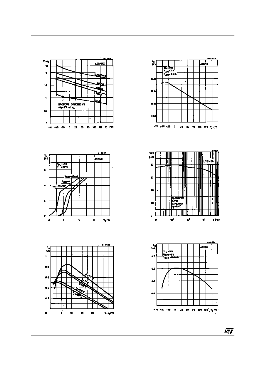
Figure 4 : Dropout Voltage vs Junction
Temperature
Figure 5 : Dropout Characteristics
Figure 6 : Peak Output Current vs Input-Output
Differential Voltage
Figure 7 : Output Voltage vs Junction
Temperature
Figure 8 : Supply Voltage Rejection vs
Frequency
Figure 9 : Quiescent Current vs Junction
Temperature

L78M00 SERIES
11/21
Figure 10 : Load Transient Response
Figure 11 : Line Transient Response
Figure 12 : Quiescent Current vs Input Voltage
L78M00 SERIES
12/21
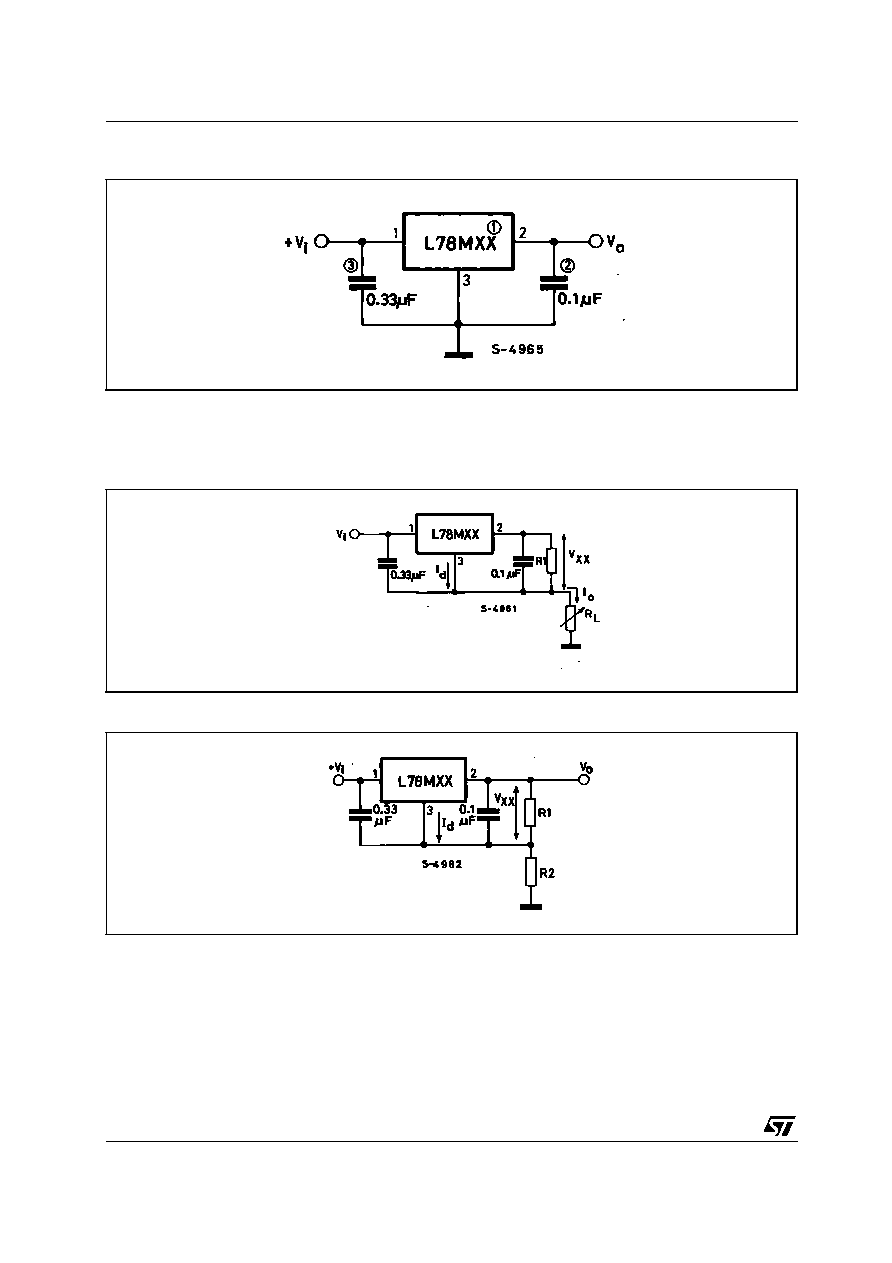
Figure 13 : Fixed Output Regulator
NOTE:
1. To specify an output voltage, substitute voltage value for "XX".
2. Although no output capacitor is need for stability, it does improve transient response.
3. Required if regulator is locate an appreciable distance from power supply filter.
Figure 14 :
Figure 15 :
V
xx
I
O
=
+ I
d
R
1
I
R1
5 Id
R
2
V
O
= V
XX
(1+
) + I
d
R
2
R
1

L78M00 SERIES
13/21
Figure 16 : Adjustable Output Regulator (7 to 30V)
Figure 17 : 0.5 to 10V Regulator
Figure 18 : High Current Voltage Regulator
Figure 19 : High Output Current with Short Circuit
R
4
V
O
= V
xx
R
1
V
BEQ1
R
1
=
I
Q1
I
REQ
-
Q1
V
BEQ1
I
O
= I
REG
+ Q
1
(I
REG
)
R
1
V
BEQ2
V
O
=
I
SC
L78M00 SERIES
14/21
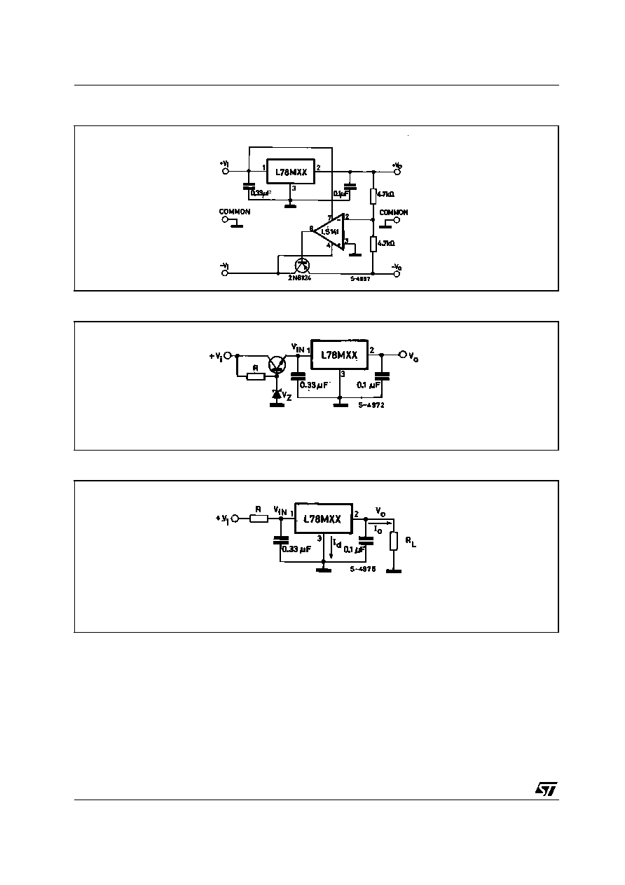
Figure 20 : Tracking Voltage Regulator
Figure 21 : High Input Voltage Circuit
Figure 22 : Reducing Power Dissipation with Dropping Resistor
V
IN
= V
I -
(V
Z
+ V
BE
)
V
I(min) -
V
XX -
V
DROP(max)
R =
I
O(max) +
I
d(max)
L78M00 SERIES
15/21
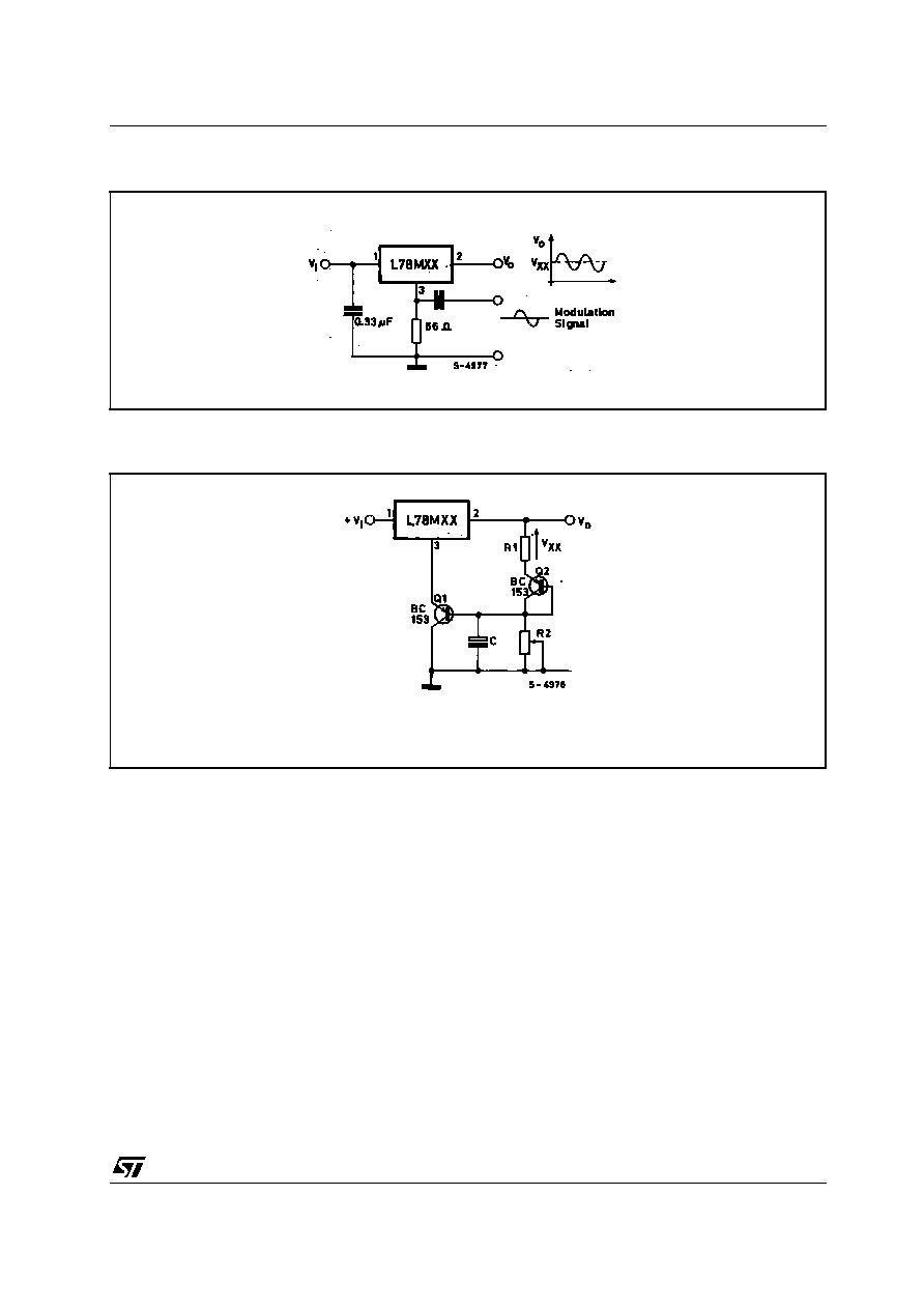
Figure 23 : Power AM Modulator (unity voltage gain, I
O
0.5)
NOTE: The circuit performs well up to 100 KHz.
Figure 24 : Adjustable Output Voltage with Temperature Compensation
NOTE: Q
2
is connected as a diode in order to compensate the variation of the Q
1
V
BE
with the temperature. C allows a slow risetime of the V
O
.
R
2
V
O
= V
XX
(1+
)
+ V
BE
R
1
L78M00 SERIES
16/21
DIM.
mm.
inch
MIN.
TYP
MAX.
MIN.
TYP.
MAX.
A
4.40
4.60
0.173
0.181
C
1.23
1.32
0.048
0.051
D
2.40
2.72
0.094
0.107
D1
1.27
0.050
E
0.49
0.70
0.019
0.027
F
0.61
0.88
0.024
0.034
F1
1.14
1.70
0.044
0.067
F2
1.14
1.70
0.044
0.067
G
4.95
5.15
0.194
0.203
G1
2.4
2.7
0.094
0.106
H2
10.0
10.40
0.393
0.409
L2
16.4
0.645
L4
13.0
14.0
0.511
0.551
L5
2.65
2.95
0.104
0.116
L6
15.25
15.75
0.600
0.620
L7
6.2
6.6
0.244
0.260
L9
3.5
3.93
0.137
0.154
DIA.
3.75
3.85
0.147
0.151
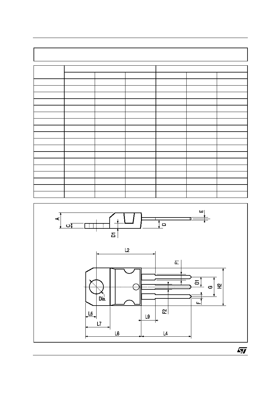
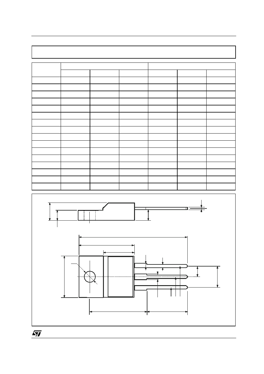
TO-220 MECHANICAL DATA
P011C
L78M00 SERIES
17/21
DIM.
mm.
inch
MIN.
TYP
MAX.
MIN.
TYP.
MAX.
A
4.40
4.60
0.173
0.181
B
2.5
2.7
0.098
0.106
D
2.5
2.75
0.098
0.108
E
0.45
0.70
0.017
0.027
F
0.75
1
0.030
0.039
F1
1.15
1.50
0.045
0.059
F2
1.15
1.50
0.045
0.059
G
4.95
5.2
0.194
0.204
G1
2.4
2.7
0.094
0.106
H
10.0
10.40
0.393
0.409
L2
16
0.630
L3
28.6
30.6
1.126
1.204
L4
9.8
10.6
0.385
0.417
L6
15.9
16.4
0.626
0.645
L7
9
9.3
0.354
0.366
DIA.
3
3.2
0.118
0.126
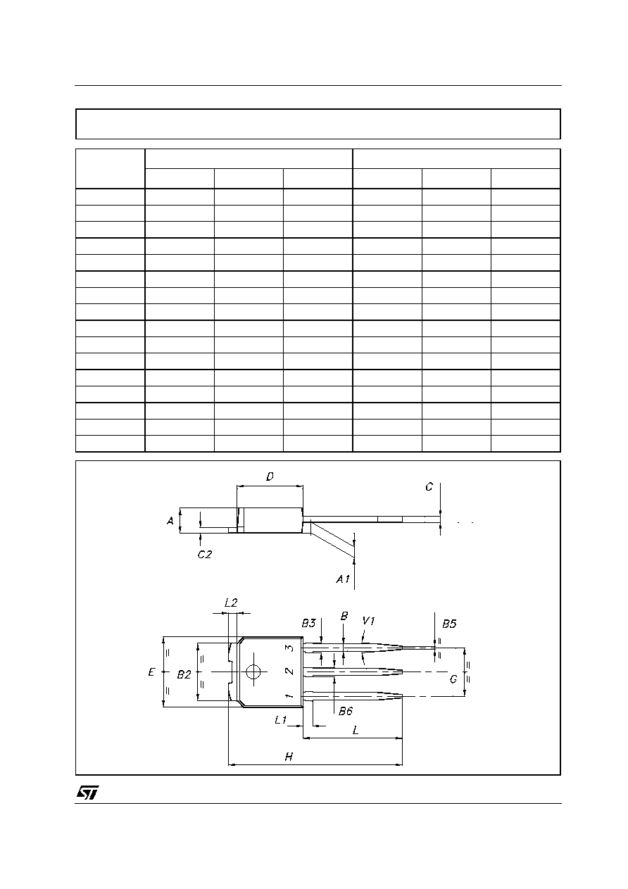
TO-220FP MECHANICAL DATA
L2
A
B
D
E
H
G
L6
Ø
F
L3
G1
1 2 3
F2
F1
L7
L4
7012510/G

L78M00 SERIES
18/21
DIM.
mm.
inch
MIN.
TYP
MAX.
MIN.
TYP.
MAX.
A
2.2
2.4
0.086
0.094
A1
0.9
1.1
0.035
0.043
A2
0.03
0.23
0.001
0.009
B
0.64
0.9
0.025
0.035
B2
5.2
5.4
0.204
0.212
C
0.45
0.6
0.017
0.023
C2
0.48
0.6
0.019
0.023
D
6
6.2
0.236
0.244
E
6.4
6.6
0.252
0.260
G
4.4
4.6
0.173
0.181
H
9.35
10.1
0.368
0.397
L2
0.8
0.031
L4
0.6
1
0.023
0.039
DPAK MECHANICAL DATA
0068772-B
L78M00 SERIES
19/21
DIM.
mm.
inch
MIN.
TYP
MAX.
MIN.
TYP.
MAX.
A
2.2
2.4
0.086
0.094
A1
0.9
1.1
0.035
0.043
B
0.64
0.9
0.025
0.035
B2
5.2
5.4
0.204
0.212
B3
0.95
0.037
B5
0.3
0.012
B6
0.95
0.037
C
0.45
0.6
0.017
0.023
C2
0.48
0.6
0.019
0.023
D
6
6.2
0.236
0.244
E
6.4
6.6
0.252
0.260
G
4.4
4.6
0.173
0.181
H
15.9
16.3
0.626
0.641
L
9
9.4
0.354
0.370
L1
0.8
1.2
0.031
0.047
L2
0.8
1
0.031
0.039
IPAK MECHANICAL DATA
0068771-F
L78M00 SERIES
20/21
DIM.
mm.
inch
MIN.
TYP
MAX.
MIN.
TYP.
MAX.
A
330
12.992
C
12.8
13.0
13.2
0.504
0.512
0.519
D
20.2
0.795
N
60
2.362
T
14.4
0.567
Ao
6.80
6.90
7.00
0.268
0.272
0.2.76
Bo
10.40
10.50
10.60
0.409
0.413
0.417
Ko
2.55
2.65
2.75
0.100
0.104
0.105
Po
3.9
4.0
4.1
0.153
0.157
0.161
P
7.9
8.0
8.1
0.311
0.315
0.319
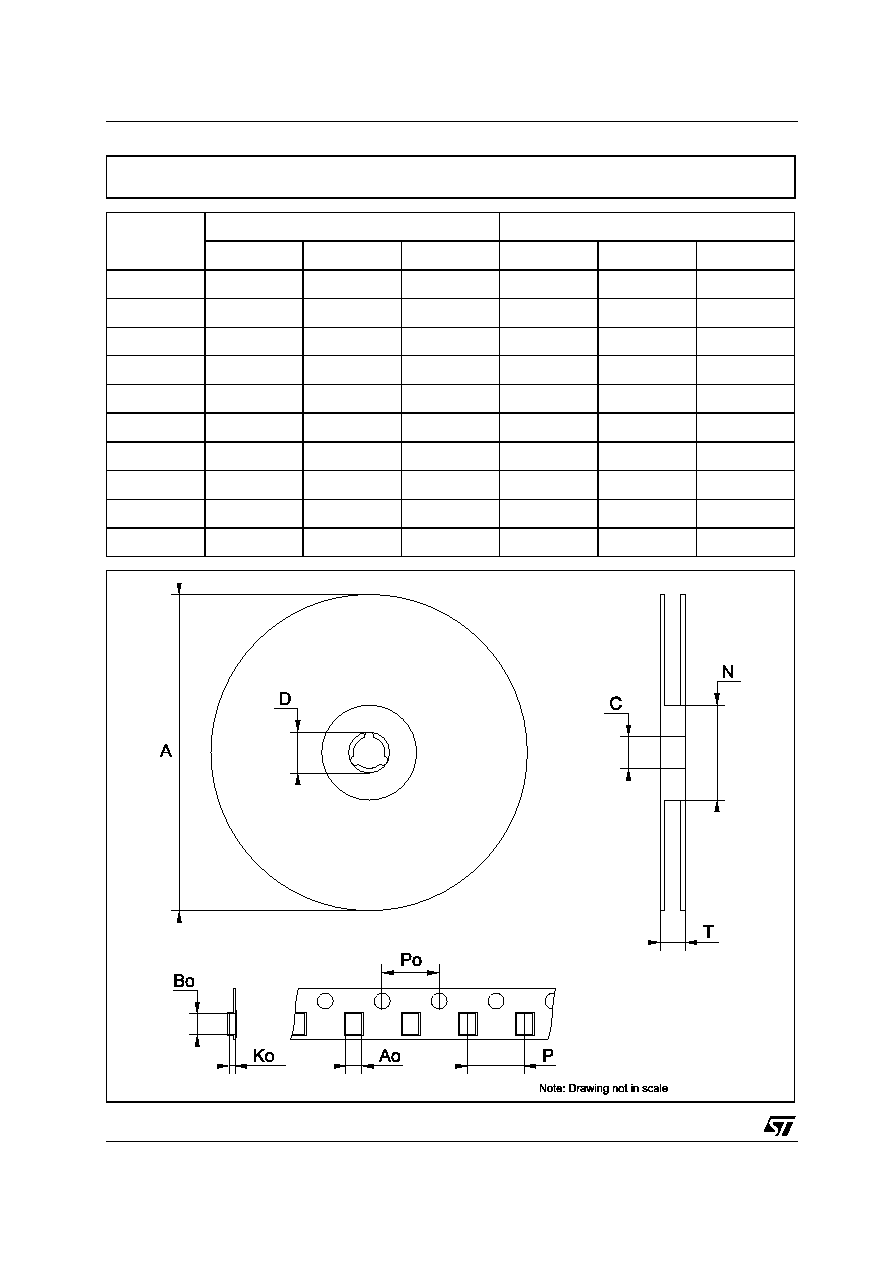
Tape & Reel DPAK-PPAK MECHANICAL DATA

L78M00 SERIES
21/21
Information furnished is believed to be accurate and reliable. However, STMicroelectronics assumes no responsibility for the
consequences of use of such information nor for any infringement of patents or other rights of third parties which may result from
its use. No license is granted by implication or otherwise under any patent or patent rights of STMicroelectronics. Specifications
mentioned in this publication are subject to change without notice. This publication supersedes and replaces all information
previously supplied. STMicroelectronics products are not authorized for use as critical components in life support devices or
systems without express written approval of STMicroelectronics.
The ST logo is a registered trademark of STMicroelectronics
All other names are the property of their respective owners
© 2003 STMicroelectronics - All Rights Reserved
STMicroelectronics GROUP OF COMPANIES
Australia - Belgium - Brazil - Canada - China - Czech Republic - Finland - France - Germany - Hong Kong - India - Israel - Italy - Japan -
Malaysia - Malta - Morocco - Singapore - Spain - Sweden - Switzerland - United Kingdom - United States.
http://www.st.com