 | –≠–ª–µ–∫—Ç—Ä–æ–Ω–Ω—ã–π –∫–æ–º–ø–æ–Ω–µ–Ω—Ç: L9333MD | –°–∫–∞—á–∞—Ç—å:  PDF PDF  ZIP ZIP |

1/13
L9333
January 2000
This is preliminary information on a new product now in development. Details are subject to change without notice.
s
WIDE OPERATING SUPPLY VOLTAGE
RANGE FROM 4.5V UP TO 32V FOR
TRANSIENT 45V
s
VERY LOW STANDBY QUIESCENT
CURRENT TYPICALLY < 2
µ
A
s
INPUT TO OUTPUT SIGNAL TRANSFER
FUNCTION PROGRAMMABLE
s
HIGH SIGNAL RANGE FROM -14V UP TO 45V
FOR ALL INPUTS
s
3.3V CMOS COMPATIBLE INPUTS
s
DEFINED OUTPUT OFF STATE FOR OPEN
INPUTS
s
FOUR OPEN DRAIN DMOS OUTPUTS, WITH
R
DSon
= 1.5
FOR V
S
> 6V AT 25
∞
C
s
OUTPUT CURRENT LIMITATION
s
CONTROLLED OUTPUT SLOPE FOR LOW EMI
s
OVERTEMPERATURE PROTECTION FOR
EACH CHANNEL
s
INTEGRATED OUTPUT CLAMPING FOR FAST
INDUCTIVE RECIRCULATION V
FB
> 45V
s
STATUS MONITORING FOR
- OVERTEMPERATURE
- DISCONNECTED GROUND OR SUPPLY
VOLTAGE
DESCRIPTION
The L9333 is a monolithic integrated quad low side
driver. It is intended to drive lines, lamps or relais in
automotive or industrial applications.
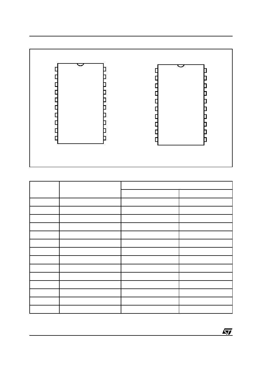
SO20 & SO20 (12+4+4)
ORDERING NUMBER:
L9333MD
(SO20 12+4+4)
L9333
(SO20)
PRODUCT PREVIEW
QUAD LOW SIDE DRIVER
BLOCK DIAGRAM
TH ER M A L
S H UT -
D OW N
D IA G-
N O S TIC
LO G IC
C H A NN E L1
C HA NN E L 4
R E F ER E NC E
V log ic
V int
IN 4
E N
VS
G ND
OU T 4
OU T 1
DIA G
4
PR G
=
&
R
EN
IN 1
R
IN
V S
PR G
R
IN
MULTIPOWER BCD TECHNOLOGY
L9333
2/13
PIN CONNECTION (Top view)
PIN FUNCTION
Pin Name
Description
Package
SO20
SO20 (SO 12+4+4)
VS
Supply Voltage
2
8
GND
Ground
9
4, 5, 6, 7, 14, 15, 16, 17
EN
Enable
6
11
PRG
Programming
15
20
DIAG
Diagnostic
19
3
IN 1
Input 1
16
1
IN 2
Input 2
17
2
IN 3
Input 3
4
9
IN 4
Input 4
5
10
OUT 1
OUTPUT 1
14
19
OUT 2
OUTPUT 2
13
18
OUT 3
OUTPUT 3
8
13
OUT4
OUTPUT4
7
12
NC
Not Connected
1,3,10,11,12,18,20
-
1
2
3
4
5
6
7
8
13
14
15
16
17
18
19
20
9
10
11
12
NC
VS
NC
IN3
IN4
EN
OUT4
OUT3
GND
NC
NC
DIAG
NC
IN2
IN1
PRG
OUT1
OUT2
NC
NC
SO
2
0
STD
1
2
3
4
5
6
7
8
13
14
15
16
17
18
19
20
9
10
11
12
IN1
IN2
DIAG
GND
GND
GND
GND
VS
IN3
IN4
PRG
OUT1
OUT2
GND
GND
GND
GND
OUT3
OUT4
EN
S
o
12
+4
+4
Me
d
.
P
o
w
e
r
3/13
L9333
ABSOLUTE MAXIMUM RATINGS
Notes: 1. In flyback phase the output voltage can reach 60V.
ESD - PROTECTION
Note: Human-Body-Model according to MIL 8832. The device widthstand ST1 class level.
THERMAL DATA
2. With 6cm
2
on board heat sink area.
3. Mounted on SMPCB2 board
Symbol
Parameter
Value
Unit
V
S
Supply voltage DC
Supply voltage Pulse (T = 400ms)
-0.3 to 32
-0.3 to 45
V
V
dV
S
/dt
Supply voltage transient
-10 to +10
V/
µ
s
V
IN
, V
EN
,
V
PRG
Input, Enable, Programming
Pin voltage
-14 to 45
V
V
OUT
Output voltage
-0.3 to 45
1)
V
V
DIAG
Diagnostic output voltage
-0.3 to 45
V
Parameter
Value
against GND
Unit
Supply pins and signal pins
±
2
KV
Output pins
±
4
KV
Symbol
Parameter
Min
Typ
Max
Unit
T
JSD
Temperature shutdown threshold
175
220
∞
C
T
JSDhys
Temperature shutdown hysteresis
20
K
SO 12+4+4
R
th (j-p)
Thermal resistance junction to pins
15
∞
C/W
R
th (j-a)
Thermal resistance junction to ambient
2)
50
∞
C/W
SO 20
R
th (j-a)
Thermal resistance junction to ambient
3)
97
∞
C/W

L9333
4/13
LIFE TIME
OPERATING RANGE:
Within the operating range the IC operates as described in the circuit description, including the diagnostic table.
ELECTRICAL CHARACTERISTCS
The electrical characteristics are valid within the defined Operating Conditions, unless otherwise specified.
The function is guaranteed by design until T
JSDon
switch-on-threshold.
Symbol
Parameter
Condition
Value
Unit
t
B
useful life time
V
S
14V
EN = low
20
years
t
b
operating life time
4.5V
V
S
32V
EN = high
5000
hours
Symbol
Parameter
Condition
Min
Max
Unit
V
S
Supply voltage
4.5
32
V
V
IN
, V
EN
,
V
PRG
Input voltage
-14
45
V
V
OUT
Output voltage
Voltage will be limited by internal Z-
Diode clamping
-0.3
60
V
V
DIAG
Diagnostic output voltage
-0.3
45
V
T
J
Junction temperature
-40
150
∞
C
Symbol
Parameter
Test Conditio n
Min.
Typ.
Max.
Unit
SUPPLY
I
Q
Quiescent current
V
S
14V; V
EN
0.3V
T
amb
85
∞
C
< 2
10
µ
A
V
S
14V; V
EN
0.3V
T
a
150
∞
C
50
µ
A
V
S
14V; EN = high, Output = off
EN = high, Output = on
1
2
3.5
mA
mA
Inputs, IN1 - IN4; Programming, PRG
V
INlow
Input voltage LOW
-14
1
V
V
INhigh
Input voltage HIGH
2
45
V
I
IN
Input current
0V
V
IN
45V
4)
-25
50
µ
A
R
IN
Input impedance
V
IN
< 0V; V
IN
> V
S
10
60
k
4. Current direction depends on the programming setting (PRG=high leads into a positive current see also Blockdiagram page 1)

5/13
L9333
Note :
All parameters are measured at 125
∞
C.
5. See also Fig.3 Timi ng Characteristics
Enable EN
V
ENlow
Input voltage LOW
-14
1
V
V
ENhigh
Input voltage HIGH
2
45
V
R
EN
Input impedance
-14V < V
EN
< 1.5V
5
k
I
EN
Input current
1.5V < V
EN
< 45V
5
80
µ
A
Output s OUT1- OUT4
R
DSon
Output ON-resistor
V
S
> 6V, I
O
= 0.3A
1.7
3.8
I
OLeak
Leakage current
V
O
= V
S
= 14V; T
a
< 125
∞
C
1
5
µ
A
V
O
= V
S
= 14V; T
a
< 150
∞
C
25
µ
A
V
OClamp
Output voltage during clamping
E
FB
2mJ; 10 mA < I
O
< 0.3A
45
52
60
V
I
OSC
Short-circuit current
V
S
> 6V
400
700
1000
mA
C
O
internal output capacities
V
O
> 4.5V
100
pF
Diagnostic Output DIAG
V
Dlow
Output voltage LOW
I
DL
= 0.6mA
0.8
V
I
Dmax
Max. output current
internal current limitation; V
D
=
14V
1
5
15
mA
I
DLeak
Leakage current
V
D
= V
S
= 14 V; T
a
< 125
∞
C
0.1
1
µ
A
V
D
= V
S
= 14 V; T
a
< 150
∞
C
5
µ
A
Timing Characteristics
5)
t
d,on
On delay time
V
S
= 14V
C
ext
= 0F; L
ext
= 0H
only testing condition
10mA
I
0
200mA
2
3.5
µ
s
t
d,off
Off delay time
3
4.5
µ
s
t
set
Enable settling time
20
µ
s
t
d,DIAG
ON or OFF Diagnostic delay time
10
µ
s
S
out
Output voltage slopes
2.5
9
16
V/
µ
s
Symbol
Parameter
Test Conditio n
Min.
Typ.
Max.
Unit
ELECTRICAL CHARACTERISTCS (continued)
L9333
6/13
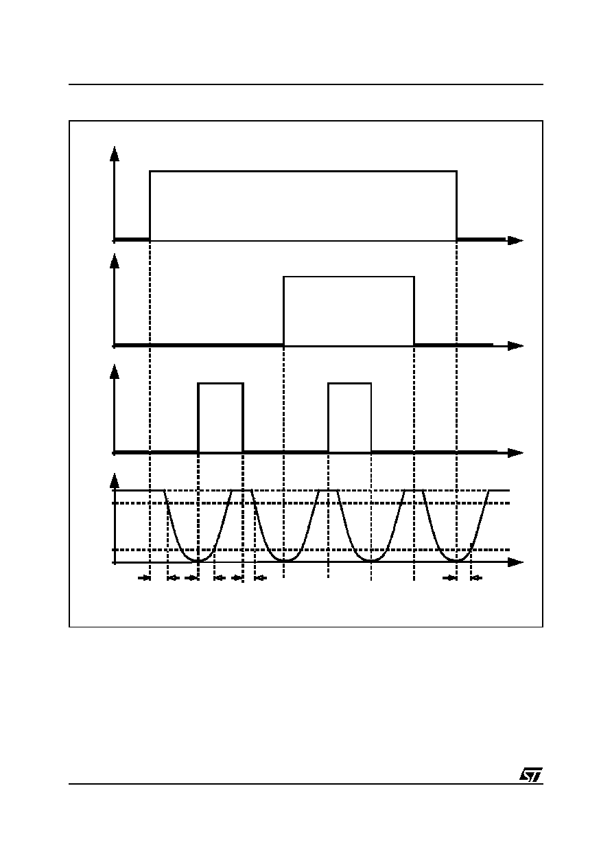
Figure 1. Timing Characteristics
6. Output voltage slope not controlled for enable low!
t
V
S
VO UT
V
IN
t
VE N
N o n - In v e r tin g M o d e
In v e r ti n g M o d e
t
set
t
d,off
t
d,on
A ctiv e
t
t
6)
VPR G
S
0.8 V
S
0.2 V
t
set
7/13
L9333
FUNCTIONAL DESCRIPTION
The L9333 is a quad low side driver for lines, lamps or inductive loads in automotive and industrial applications.
The logic input levels are 3.3V CMOS compatible. This allows the device to be driven directly by a microcon-
troller. For the noise immunity, all input thresholds have a hysteresis of typ. 100mV. Each input (IN, EN and
PRG) is protected to withstand voltages from -14V to 45V. The device is activated with a 'high' signal on ENable.
ENable 'low' switches the device into the sleep mode. In this mode the quiescent current is typically less than
2
µ
A. A high signal on PRoGramming input changes the signal transfer polarity from noninverting to the inverting
mode. This pin can be connected either to V
S
or GND. If these pins are not connected, the forced status of the
PRG and EN pin is low. For packaged applications it is still recommended to connect all input pins to ground
respective VS to avoid EMC influence. The forced condition leads to a mode change if the PRG pin was high
before the interruption. Independent of the PRoGramming input, the OUTput switches off, if the signal INput pin
is not connected. This function is verified using a leakage current of 5
µ
A (sink for PRG=high; source for
PRG=low) during circuit test.
Each output driver has a current limitation of min 0.4A and an independent thermal shut-down. The thermal
shut-down deactivates that output, which exceeds temperature switch off level. When the junction temperature
decreases 20K below this temperature threshold the output will be activated again. This 20K is the hysteresis
of the thermal shutdown function. The Gates, of the output DMOS transistors are charged and discharged with
a current source. Therefore the output slope is limited. This reduces the electromagnetic radiation. For induc-
tive loads an output voltage clamp of typically 52V is implemented.
The DIAGnostic is an open drain output. The logic status depends on the PRoGramming pin. If the PRG pin is
'low' the DIAG output becomes low, if the device works correctly. At thermal shut-down of one channel or if the
ground is disconnected the DIAGnostic output becomes high. If the PRG pin is 'high' this output is switched off
at normal function and switched on at overtemperature. For the fault condition of interrupted ground, the poten-
tial of VS and Diagnostic should be equal.
DIAGNOSTIC TABLE
X = not relevant
* selective for each channel at overtemperature
Pins
EN
PRG
IN
OUT
DIAG
Normal function
H
L
L
L (on)
L (on)
H
L
H
H (off)
L (on)
H
H
L
H (off)
H (off)
H
H
H
L (on)
H (off)
L
X
X
H (off)
H (off)
Overtemperature,
disconnected ground or
supply voltage
H
L
X
H (off)
*
H (off)
Overtemperature
H
H
X
H(off)
*
L(on)
L9333
8/13
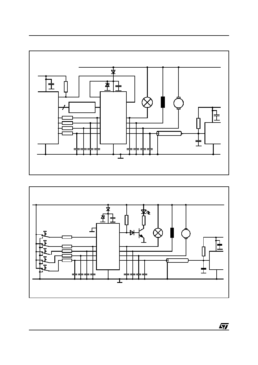
Figure 2. Application for Inverting Transfer Polarity
Figure 3. Application for non Inverting Transfer Polarity
Note We recommend to use the device for driving inductive loads with flyback energy E
FB
2mJ.
IN
OUT 1
OUT 2
OUT 3
OUT 4
IN 1
IN 2
IN 3
IN 4
GND
VS
PRG
EN
DIAG
Adressdecoder
A 0:8
D 0
D 1
D 2
D 3
8
VCC = 5V or 3.3V
VCC
GND
M
I
CRO
CO
NT
RO
L
L
E
R
INT
BOARD VOLTAGE 14 V
2 W
12 mH
250 mA
50 kHz
VCC
GND
VCC = 5V
33
µ
F
240
50pF
10
µ
H
L9333
M
IN
BOARD VOLTAGE 14 V
2 W
12 mH
250 mA
10
µ
H
VCC
GND
VCC = 5V
OUT 1
OUT 2
OUT 3
OUT 4
IN 1
IN 2
IN 3
IN 4
GND
VS
PRG
EN
DIAG
L9333
240
50pF
M
33
µ
F
9/13
L9333
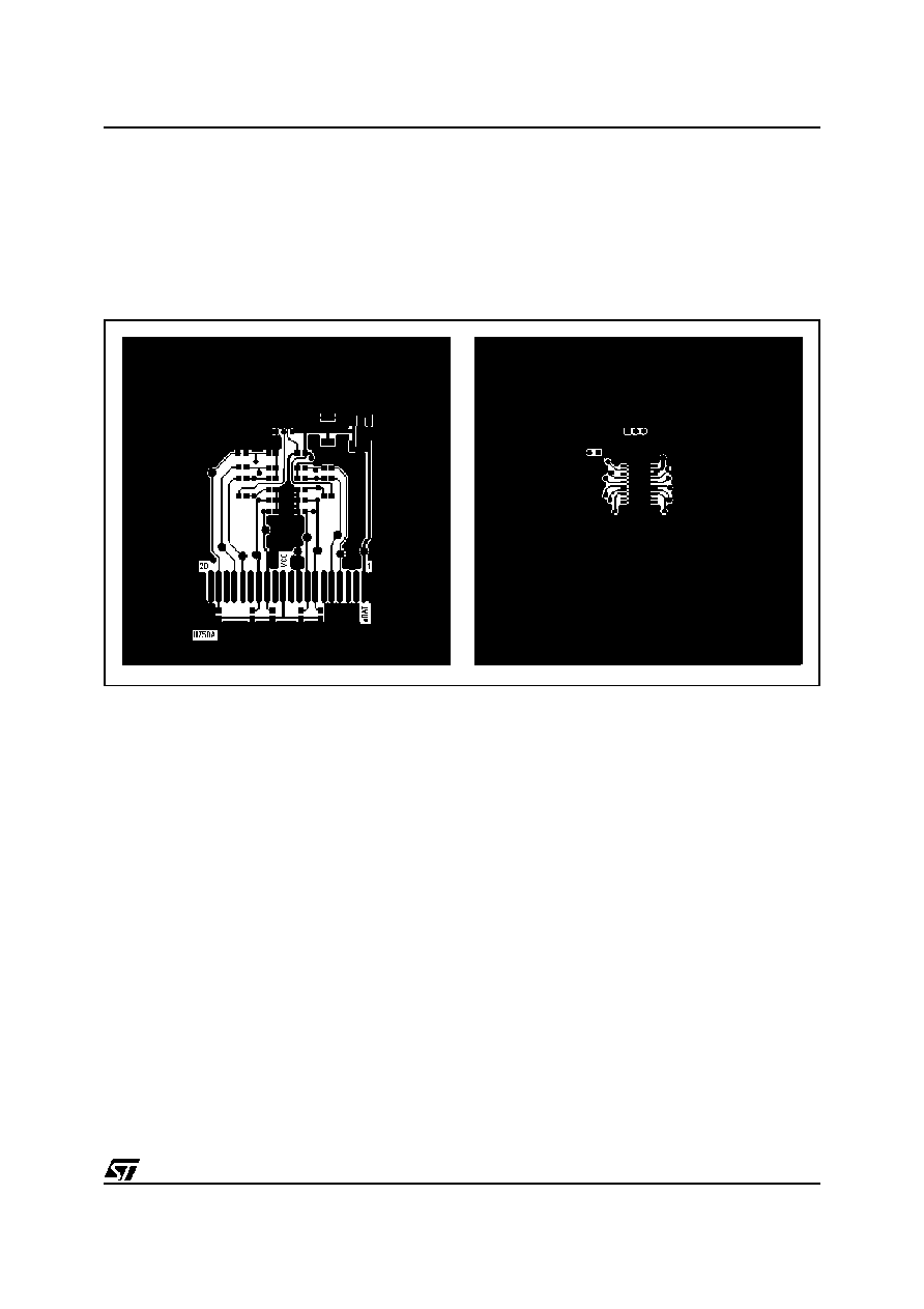
EMC SPECIFICATION
EMS (electromagnetic susceptibility)
Measurement setup:
DUT mounted on a specific application board is driven in a typical application circuit (see below). Two devices
are stimulated by a generator to read and write bus signals. They will be monitored externally to ensure proper
function.
Figure 4. PCB layout
Measurement method:
a)
The two bus lines are transferred 2m under a terminated stripline. That's where they were exposed to the
RF-field. Stripline setup and measurement method is described in DIN 40839-4 or ISO 11452-5.
b)
DUT mounted on the same application board is exposed to RF through the tophole of a TEM-cell. Mea-
surement method according SAE J1752.
c)
The two bus lines are transferred into a BCI current injection probe. Setup and measurement method is
described in ISO 11452-4.
Failure criteria:
Failure monitoring is done by envelope measurement of the logic signals with a LeCroy oscilloscope with ac-
ceptance levels of 20% in amplitude and 2% time.
Limits:
The device is measured within the described setup and limits without fail function.
The Electromagnetic Susceptivity is not tested in production.
a) Field strength under stripline of > 250V/m in the frequency range 1 - 400MHz modulation:AM 1kHz 80%.
b) Field strength in TEM-cell of > 500V/m in the frequency range 1 - 400MHz modulation:
AM 1kHz 80%.
c) RF-currents with BCI of > 100mA in the frequency range 1 - 400MHz modulation:
AM 1kHz 80%.
TOPSIDE
BACKSIDE
L9333
10/13
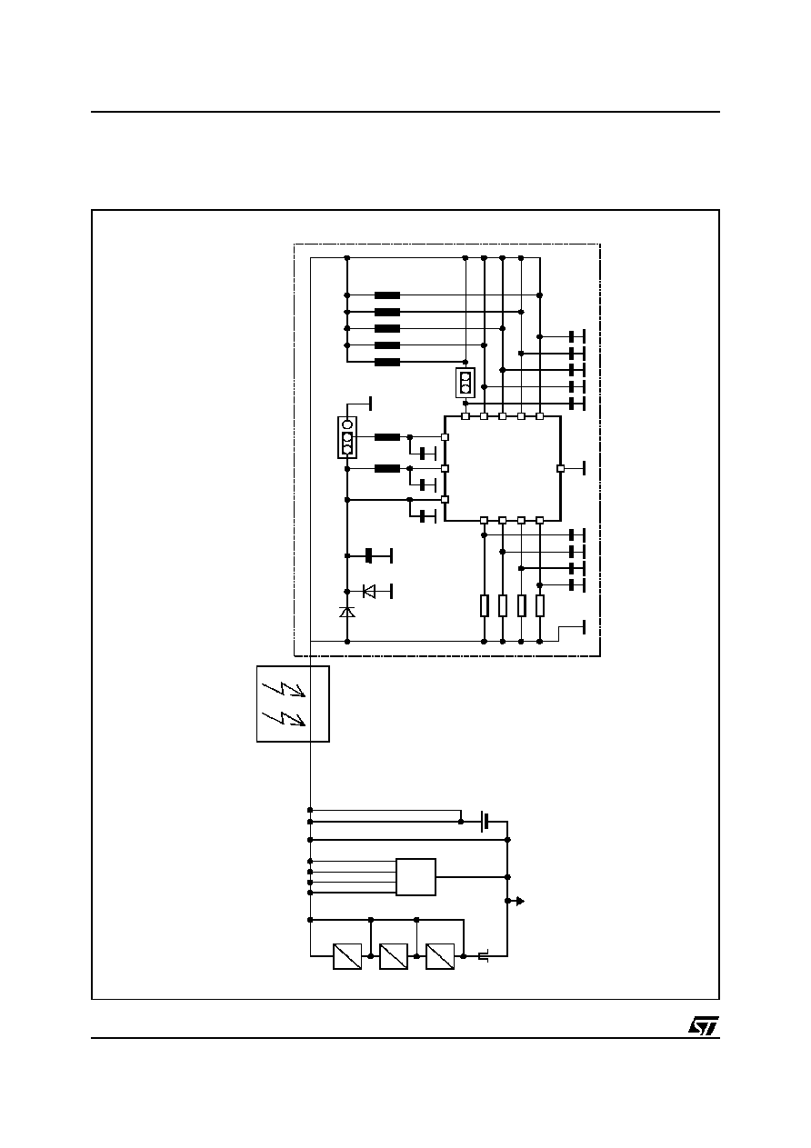
Measured Circuit
The EMS of the device was verified in the below described setup.
Figure 5.
2m
St
ri
p
l
i
n
e
f
2
16
7
8
13
9
1
11
12
5
H
z
25
0
H
z
50
0
H
z
17
4
5
1k
H
z
f
2
f
2
+
-
14
U(
t
)
14V
F
l
at
c
abl
e
A
N
E
CHO
I
C
CH
A
M
B
E
R
J
u
mper
SM
BYW0
1
-
2
0
0
S
M
6
T
39A
33
µ
F
10n
F
10k
4.
7n
F
4
.
7
nF
10
k
20k
4
4.
7
n
4.
7n
F
4
1n
F
o
p
t
i
ona
l
V
S
EN
PR
G
DI
A
G
OU
T
1
OU
T
2
OU
T
3
OU
T
4
IN
1
IN
2
IN
3
IN
4
GN
D
L9333
4
10k
4
10
0
o
p
t
i
ona
l
1
16
17
4
5
9
11
19
14
13
8
7
J
u
m
per
11/13
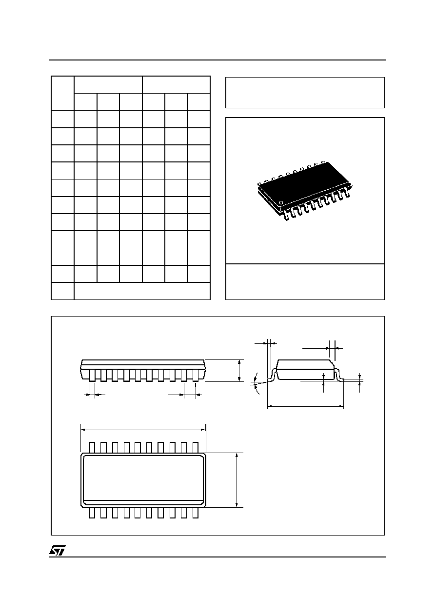
L9333
1
1
0
11
20
A
e
B
D
E
L
K
H
A1
C
SO20MEC
h x 45
∞
SO20
DIM.
mm
inch
MIN.
TYP.
MAX.
MIN.
TYP.
MAX.
A
2.35
2.65
0.093
0.104
A1
0.1
0.3
0.004
0.012
B
0.33
0.51
0.013
0.020
C
0.23
0.32
0.009
0.013
D
12.6
13
0.496
0.512
E
7.4
7.6
0.291
0.299
e
1.27
0.050
H
10
10.65
0.394
0.419
h
0.25
0.75
0.010
0.030
L
0.4
1.27
0.016
0.050
K
0
∞
(min.)8
∞
(max.)
OUTLINE AND
MECHANICAL DATA
L9333
12/13
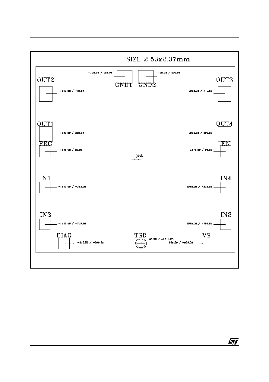
PAD
L9333

Information furnished is believed to be accurate and reliable. However, STMicroelectronics assumes no responsibility for the consequences
of use of such information nor for any infringement of patents or other rights of third parties which may result from its use. N o license is granted
by implication or otherwise under any patent or patent rights of STMicroelectronics. Specifications mentioned in this publication are subject
to change without notice. This publication supersedes and replaces all information previously supplied. STMicroelectronics products are not
authorized for use as critical components in life support devices or systems without express written approval of STMicroelectronics.
The ST logo is a registered trademark of STMicroelectronics
Æ
2000 STMicroelectronics - All Rights Reserved
STMicroelectronics GROUP OF COMPANIES
Australia - Brazil - China - Finland - France - Germany - Hong Kong - India - Italy - Japan - Malaysia - Malta - Morocco - Singapore - Spain
- Sweden - Switzerland - United Kingdom - U.S.A.
http:/ /www.st.com
13/13
L9333