 | –≠–ª–µ–∫—Ç—Ä–æ–Ω–Ω—ã–π –∫–æ–º–ø–æ–Ω–µ–Ω—Ç: L9616D | –°–∫–∞—á–∞—Ç—å:  PDF PDF  ZIP ZIP |
L9616
HIGH SPEED CAN BUS TRANSCEIVER
L9616 MEETS ISO/DIS 11898 UP TO
1MEGABAUD
TRANSMITTER
- GENERATION OF DIFFERENTIAL OUTPUT
SIGNALS
- SHORT CIRCUIT PROTECTED FROM -5V
TO 36V, DETECTION & SHUTDOWN
- SLOPE CONTROL TO REDUCE RFI AND EMI
- TWO STATES ADJUSTABLE SLOPE
CONTROL (
1MEGABAUD/
250KBAUD)
RECEIVER
- DIFFERENZIAL INPUT WITH HIGH
INTERFERENCE SUPPRESSION
- COMMON MODE INPUT VOLTAGE RANGE
(V
COM
) FROM -2V TO V
S
+3V
ESD PROTECTION LEVEL UP TO 4kV
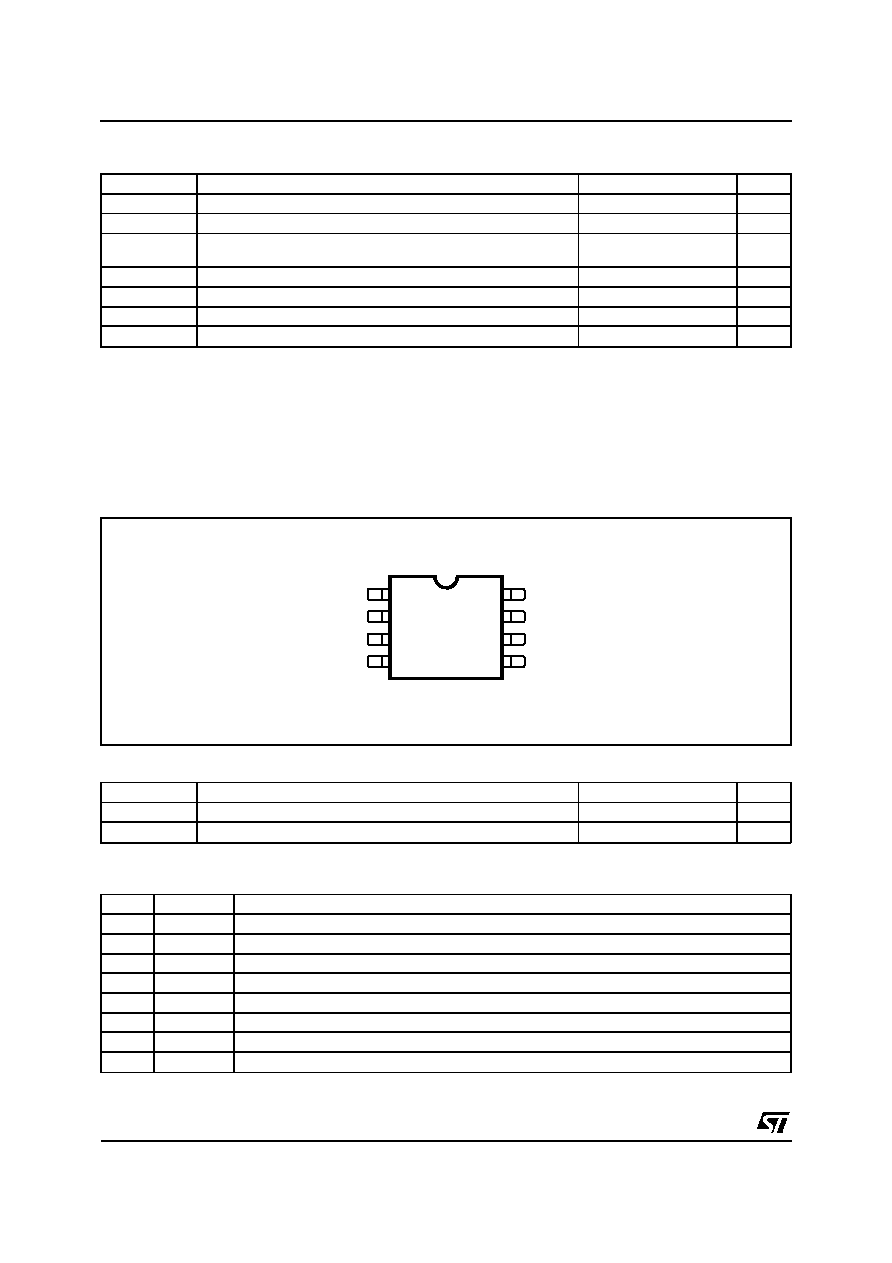
PACKAGE: SO-8
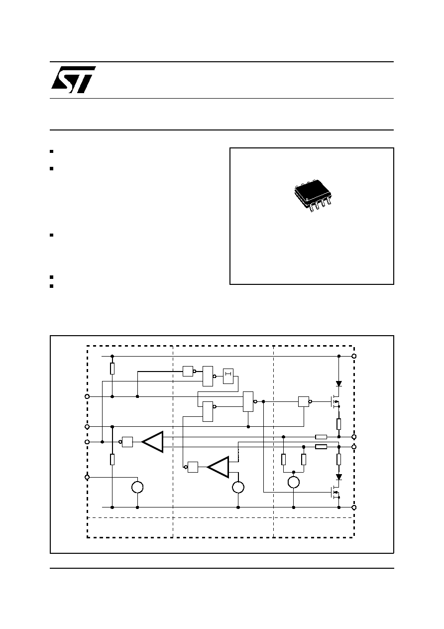
DESCRIPTION
The L9616 is a bidirectional transceiver for signal
conditioning and processing in connection with a
CAN controller. Data rates of up to 1MEGABAUD
are supported using either shielded or non-
shielded pair of lines.
November 2000
Æ
1
&
RX0
TX0
RX1
V
S
C_H
C_L
D96AT245
1
V
S
+
-
td
1
&
1
1
+
-
M
M
M
GND
3
7
6
2
ASC
V
REF
V
CLmax
1
8
4
5
RECEIVER
PROTECTION
TRANSMITTER
BLOCK DIAGRAM
SO-8
ORDERING NUMBER: L9616D
1/8
ABSOLUTE MAXIMUM RATINGS
Symbol
Parameter
Value
Unit
V
S
Supply Voltage
-0.3 to 7
V
V
C_H
, V
C_L
Bus Voltage at C_H, C_L (VS 0 to 5.5V)
-5 to 36
V
I
C_H
, I
C_L
Off State Leakage Current at C_H, C_L ( VS =0 to 5.5V,
V
C_H
= -5 to 36V, V
C_L
= -5 to 36 )
-3 to 5
mA
V
DC
DC Voltage at TXO, ASC (VS 0 to 5.5V)
GND -0.3 to V
S
+0.3
V
I
RXO
Output Current at RXO (V
S
0 to 5.5V)
-0.3 to 1
mA
T
stg
, T
J
Storage and Junction Temperature Range
-40 to 150
∞C
T
op
Operating Temperature Range
-40 to 125
∞C
All voltages, except bus voltage, are defined with respect to pin 2
Positive currents flow into the IC.
THERMAL DATA
Symbol
Parameter
Value
Unit
PIN FUNCTIONS
N.
Name
Function
1
TXO
Transmitter Input
2
GND
Ground
3
V
S
Supply Voltage
4
RXO
Receive Output
5
RX1
Reference Voltage
6
C_L
Low Side Bus Output
7
C_H
High Side Bus Output
8
ASC
Adjustable Slope Control
TX0
GND
V
S
RX0
RX1
C_L
C_H
ASC
1
3
2
4
6
5
7
8
D96AT246
PIN CONNECTION
L9616
2/8
ELECTRICAL CHARACTERISTICS (T
OP
= -40 to 125∞C; V
S
= 4.5 to 5.5V; Dominat: VTXO = GND; Re-
cessive: VTXO = V
S
; All voltages, except bus voltage, are defined with respect to pin 2. Positive currents
flow into the IC unless otherwise specified.)
Symbol
Parameter
Test Condition
Min.
Typ.
Max.
Unit
V
S
Supply Voltage
4.5
5
5.5
V
I
S
Supply Current
Dominant
80
mA
Recessive
20
mA
TRANSMITTER SECTION (R
A
= 60
between C_H and C_L)
C
TXO
TXO Input Capacitance
0V < V
TXO
< V
S
25
pF
V
TXO
TXO High Level Input Voltage
0.7 V
S
V
S
TXO Low Level Input Voltage
0
0.3 V
S
I
TXO
TXO High Level Input Current
V
TXO
= V
S
-2
0
2
µ
A
TXO Low Level Input Current
V
TXO
= GND
-275
0
-25
µ
A
C
ASC
ASC Input Capacitance
0V < V
ASC
< V
S
25
pF
V
ASC
ASC Input Voltage for High
Speed
0
0.1 V
S
ASC Input Voltage for Low Speed
0.9 V
S
VS
I
ASC
ASC Input Current
V
ASC
= V
S
25
275
µ
A
V
ASC
= 0V
-2
0
2
µ
A
V
C_H
, V
C_L
Bus Voltage Recessive
Recessive
0.4 V
S
0.5 Vs
0.6 Vs
I
C_H
, I
C_L
Leakage Current Recessive
VC_L = V
C_H
= -2 to 7V
-0.7
0.7
mA
V
C_L
= V
C_H
= 1 to 4V
-0.3
0.3
mA
R
IN(C_H
,
C_L)
Input Resistence
Recessive
5
50
K
R
Diff(C_H
,
C_L)
Differential Input Resistence
Recessive
10
100
K
V
Diff
=
V
C_H
- V
C_L)
Differential Output Voltage
Dominant, R
A
1.5
3
V
V
Diff
=
V
C_H
- V
C_L)
Differential Output Voltage
Recessive
-500
0
50
mV
t
d
Short Circuit Detection Time
C_H to C_L ; C_H to B
R
CS
< 1
1
5
10
µ
s
I
A
Supply Current in Case of Short
Circuit, C_H to C_L, C_H to B
(time = t
d
)
150
mA
V
C_Lmax
Overvoltage Protection
Threshold on C_L
7
8
10
V
RECEIVE SECTION
V
RXO
RXO High Level Output Voltage
V
Diff
< 0.5V; I
RXO
= 0.3mA;
V
C_H
= -2 to 7V; V
C_L
= -2 to 7V;
0.9 V
S
Vs
V
RXO Low Level Output Voltage
V
Diff
> 0.9V; I
RXO
= 1mA;
V
C_H
= -2 to 7V; V
C_L
= -2 to 7V;
0.5
V
V
S
=
V
C_H
-V
C_L
Input Signal Threshold
V
C_H
= -2 to 7V; V
C_L
= -2 to 7V;
500
700
900
mV
V
COM
= (V
C_H
+V
C_L
)/2
Input Common Mode Voltage
Range
-2
7
V
V
HYS
Differential Input Hysteresis
150
mV
REFERENCE OUTPUT
V
RX1
Reference Voltage
I
RX1
= 0
0.45 V
S
0.5 V
S
0.55 V
S
V
R
RX1
Output Resistance
2
9
K
L9616
3/8
FUNCTIONAL DESCRIPTION
The L9616 is used as an interface between a
CAN controller and the physical bus. The device
provides transmitting capability to the CAN con-
troller.
The transmitter outputs C_H and C_L are pro-
tected against short circuits and electrical tran-
sients which may occur in an automotive environ-
ment. In case of short circuit (C_H to C_L, C_H to
B) the protection circuit recognizes this fault con-
ditionand the transmitter output stages are dis-
abled with a delay of max. 10
µ
s to prevent de-
struction of the IC and high consumption of
supply current I
S
. If V
C_L
>V
C_Lmax
the transmitter
output stages would be disabled immediately.
Pin ASC makes it possible to select two different
modes of operation: High speed (
1MEGABaud)
and low speed (
250kBaud).
The ASC pin is tied to GND for normal operation
at
1MEGABaud. For slower speed operation at
250kBaud the rise and fall slope of the bus out-
put can be decreased to reduce EMI by connect-
ingg the ASC pin to V
S
.
FUNCTIONAL TABLE
TXO
C_H
C_L
Bus State
RXO
L
H
L
Dominant
L
H or
Floating
Floating
V
S
/2
Floating
V
S
/2
Recessive
H
DINAMIC CHARACTERISTICS (C
A
= 47pF between C_H and C_L; V
S
= 5V; t
R
< 5ns;
C
RXO
= 20pF between RXO and B; R
A
= 60
between C_H and C_L)
Symbol
Parameter
Test Condition
Min.
Typ.
Max.
Unit
t
OT
Signal Delay TXO to C_H, C_L
50
ns
S
R
Differential Output Slew Rate
(Transmitter)
V
ASC
= 0V
20
50
V/
µ
s
V
ASC
= V
S
5
20
V/
µ
s
t
OR
Signal Delay C_H, C_L to R
XO
V
ASC
= 0V
150
ns
t
OTR
Signal Delay T
XO
to R
XO
V
ASC
= 0V
300
ns
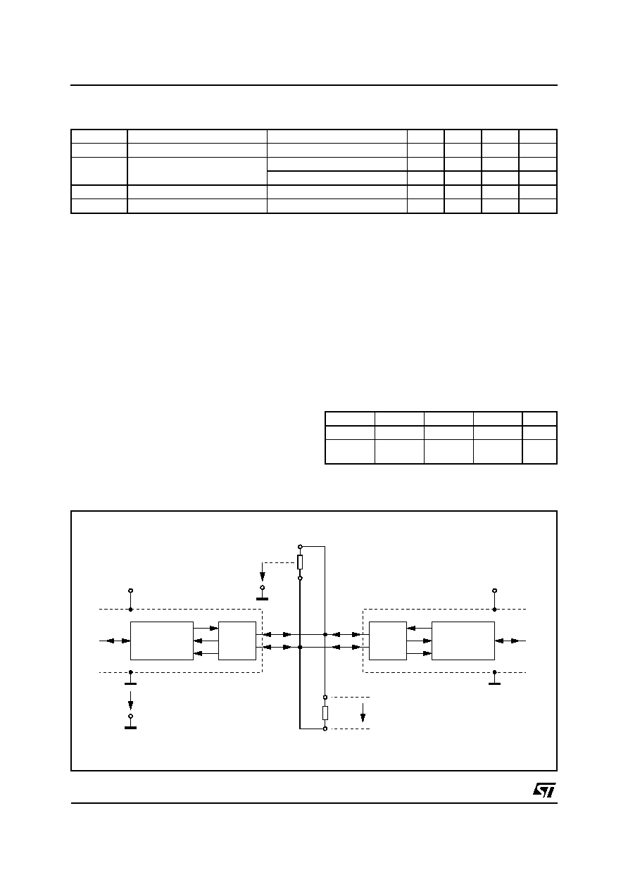
CONTROLLER
L9615
L9615
CONTROLLER
CAN BUS
SYSTEM n
V
COM
R
A
V
Sn
V
GNDn
V
GNDD
V
GNDm
R
A
V
Diff
C_H
C_L
SYSTEM m
V
GNDm
V
Sm
D96AT247A
TYPICAL APPLICATION
L9616
4/8
t
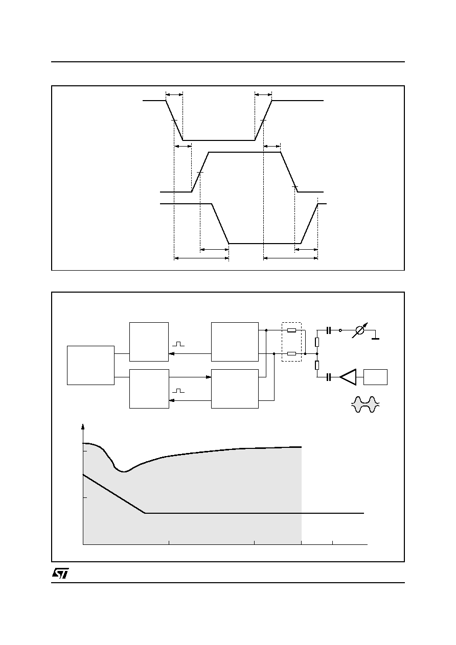
OTR
t
OTR
t
OR
t
OR
0.5V
0.9V
t
OT
t
OT
t
R
t
R
V
TX0
V
Diff
V
RX0
D96AT248
TIMING DIAGRAM
MONITORING
(BIT COMPARISON)
CAN
CONTROLLER
1
CAN
CONTROLLER
2
CAN
TRANSCELVER
1
CAN
TRANSCELVER
2
250Kbit/sec
250Kbit/sec
HP8640
30
30
EQUIVALENT TERMINATING
RESISTOR 2 x 120
PARALLEL AT LINE ENDS
6.8
µ
F
6.8
µ
F
100
450
Ust (Noise signal)
50
40dB
90%AM, 1KHz
10MHz
1MHz
100MHz
500MHz
1GHz
NOISE RESISTANT
NOT NOISE RESISTANT
min. request boundary
(automotive industry)
U
ST
(V)
30V
SS
20V
SS
10V
SS
D96AT249C
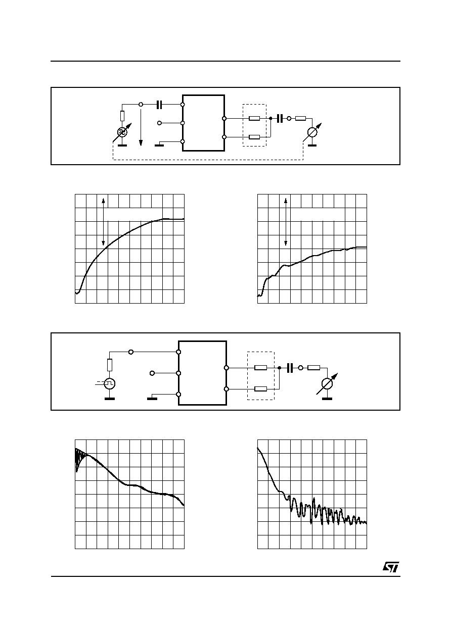
EMC PERFORMANCE (RECEIVER)
L9616
5/8
50
80dB
µ
F
30
30
50
4.7nF
µ
V
TEK495
Analyzer
equivalent terminating resistor
2 x 120
parallel at line ends
4.7nF
+5V
TX0
GND
V
S
C_H
C_L
D96AT250
EMC PERFORMANCE (TRANSMITTER)
0
40
80
120
160
f(KHz)
D96AT251
0
10
20
30
40
50
60
70
80
1
3.162
10
31.62
100
316.2
1000
3162
10000
ATTENUATION OF
TRANSMITTER
Transceiver Without Emc Reducing Measures
0
40
80
120
160
f(KHz)
D96AT252
0
10
20
30
40
50
60
70
80
1
3.162
10
31.62
100
316.2
1000
3162
10000
ATTENUATION OF
TRANSMITTER
Transceiver With Emc Reducing Measures
50
250KHz
30
30
50
4.7nF
µ
V
TEK495
Analyzer
equivalent terminating resistor
2 x 120
parallel at line ends
+5V
TX0
GND
V
S
C_H
C_L
D96AT253
5V
EMC PERFORMANCE (Transceiver Sending)
0
40
80
120
160
f(KHz)
D96AT254
0
10
20
30
40
50
60
70
80
1
3.162
10
31.62
100
316.2
1000
3162
10000
Transceiver Without Emc Reducing Measures
0
40
80
120
160
f(KHz)
D96AT255
0
10
20
30
40
50
60
70
80
1
3.162
10
31.62
100
316.2
1000
3162
10000
Transceiver With Emc Reducing Measures
L9616
6/8
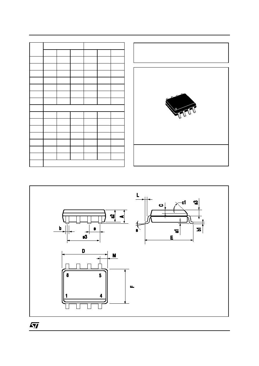
DIM.
mm
inch
MIN.
TYP.
MAX.
MIN.
TYP.
MAX.
A
1.75
0.069
a1
0.1
0.25
0.004
0.010
a2
1.65
0.065
a3
0.65
0.85
0.026
0.033
b
0.35
0.48
0.014
0.019
b1
0.19
0.25
0.007
0.010
C
0.25
0.5
0.010
0.020
c1
45
∞
(typ.)
D (1)
4.8
5.0
0.189
0.197
E
5.8
6.2
0.228
0.244
e
1.27
0.050
e3
3.81
0.150
F (1)
3.8
4.0
0.15
0.157
L
0.4
1.27
0.016
0.050
M
0.6
0.024
S
8
∞
(max.)
(1) D and F do not include mold flash or protrusions. Mold flash or
potrusions shall not exceed 0.15mm (.006inch).
SO8
OUTLINE AND
MECHANICAL DATA
L9616
7/8

Information furnished is believed to be accurate and reliable. However, STMicroelectronics assumes no responsibility for the consequences
of use of such information nor for any infringement of patents or other rights of third parties which may result from its use. No license is
granted by implication or otherwise under any patent or patent rights of STMicroelectronics. Specification mentioned in this publication are
subject to change without notice. This publication supersedes and replaces all information previously supplied. STMicroelectronics products
are not authorized for use as critical components in life support devices or systems without express written approval of STMicroelectronics.
The ST logo is a registered trademark of STMicroelectronics
© 2000 STMicroelectronics ≠ Printed in Italy ≠ All Rights Reserved
STMicroelectronics GROUP OF COMPANIES
Australia - Brazil - China - Finland - France - Germany - Hong Kong - India - Italy - Japan - Malaysia - Malta - Morocco -
Singapore - Spain - Sweden - Switzerland - United Kingdom - U.S.A.
http://www.st.com
L9616
8/8