 | –≠–ª–µ–∫—Ç—Ä–æ–Ω–Ω—ã–π –∫–æ–º–ø–æ–Ω–µ–Ω—Ç: L9703D | –°–∫–∞—á–∞—Ç—å:  PDF PDF  ZIP ZIP |
L9703
March 1992
OCTAL GROUND CONTACT MONITORING CIRCUIT
.
OPERATING DC SUPPLY VOLTAGE RANGE
5V TO 25V
.
SUPPLY OVERVOLTAGE PULSE UP TO 40V
.
VERY LOW STANDBY QUIESCENT CUR-
RENT 0.2mA
.
INTERNAL CLAMPING DIODES AT CONTACT
INPUTS TO V
S
AND GND
.
INPUT PULSE CURRENT CAPABILITY UP TO
+ 50mA ; ≠ 75mA
.
NOMINAL CONTACT CURRENT OF 10mA DE-
FINED BY EXTERNAL CONTACT SERIES RE-
SISTORS R
I N1≠8
.
CONTACT STATUS MONITORING BY COM-
PARING THE RESISTANCE AT CONTACT
SENSE INPUTS WITH THE INTERNAL REFER-
ENCE RESISTOR VALUE
.
HIGH IMMUNITY DUE TO RESISTANCE COM-
PARISON WITH HYSTERESIS
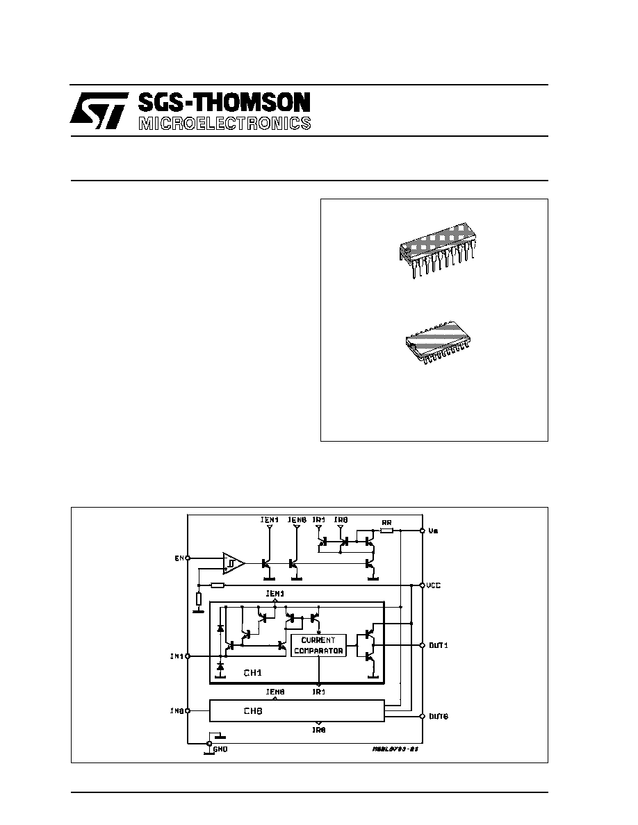
BLOCK DIAGRAM
SO-20L
DIP-20
ORDERING NUMBERS : L9703 (DIP-20)
L9703D (SO-20L)
DESCRIPTION
The L9703 is a bipolar monolithic integrated cir-
cuit for monitoring the status of up to eight con-
tacts connected to GND.
It contains eight contact sense inputs and eight
microcomputer compatible three-state outputs.
1/9

PIN CONNECTION (top view)
ABSOLUTE MAXIMUM RATINGS
Symbol
Parameter
Test Conditions
Unit
V
S
Transient Supply Voltage (t
1s)
+40
V
V
CC
Logic Supply Voltage
7
V
I
IN DC
Input DC Current
±
40
mA
I
INP
Input DC Pulse
(test pulse specification: 0 < tP < 2ms, f
0.2Hz, n = 25000)
50
-75
mA
mA
I
O
Output Current
Internally Limited
V
EN
Enable Input Voltage
V
CC
+0.3
-0.3
V
V
P
O
Power Dissipation at T
amb
= 80
∞
C
DIP20
SO20
875
420
mW
mW
T
stg,
T
J
Storage and Junction Temperature Range
-55 to 150
∞
C
THERMAL DATA
Symbol
Parameter
DIP20
SO20
Unit
R
th j-amb
Thermal Resistance Junction to Ambient
MAX.
80
165
∞
C/W
L9703
2/9
ELECTRICAL CHARACTERISTICS (5V
V
S
25V; -40
∞
C
T
j
125
∞
C; 4.75V
V
CC
5.25V unless oth-
erwise specified; the currents flowing in the arrow direction are assumed positive as marked in the application
circuit diagram, fig. 1).
Symbol
Parameter
Test Conditions
Min.
Typ.
Max.
Unit
V
ENL
Enable Input Voltage LOW
(device activated)
0.8
V
V
ENH
Enable Input Voltage HIGH
2.4
V
V
EN hyst
Enable Input Hysteresis
200
420
800
mV
I
EN
Enable Input Current
2.4V < V
EN
< V
CC
5
µ
A
0V < V
EN
< 0.8V
-5
-1
µ
A
V
OUTH
Output Voltage HIGH
0 < I
OUT
< 100
µ
A
4.0
V
CC
-0.1
V
CC
V
V
OUTL
Output Voltage LOW
I
OUT
= -1mA
0.05
0.2
0.4
V
I
OUT TS
Output TRISTATE Current
0 < V
OUT
< V
CC
0.5
µ
A
V
IN
Input Voltage (device active)
EN = LOW
R
IN
= 1k
V
S
- 2
V
S
- 1.5
V
S
- 0.4
V
V
IN
Input Clamped Voltage
(device disabled)
EN = HIGH
I
IN
= 30mA
I
IN
= -30mA
V
S
+ 0.3
-2
V
S
+ 1
-1
V
S
+ 2
-0.3
V
V
I
OUT
Output Current
OUT = HIGH
V
OUT
= 0
2
mA
I
OUT
Output Current
OUT = LOW
VOUT = 5.5V
-20
mA
R
IL
Input Resistor (note 1)
LOW Threshold
5V < V
S
< 16V
V
GND
0.1V
S
1.8
4
K
R
IH
Input Resistor (note 1)
HIGH Threshold
5.3
20
K
Input Resistor
Threshold Ratio (note1)
0.65
0.75
0.85
I
QC
Quiescent Current
EN = HIGH (t
ENH
80
µ
s)
5V < V
S
< 16V
-40
∞
C
T
j
100
∞
C
0.12
0.16
mA
I
QS
Quiescent Current
All Inputs Open
0.04
mA
All Inputs Closed
0.24
mA
I
QC
I
QS
Quiescent Current
EN = LOW
6
6
mA
mA
t
do
Delay Time/Output
(EN LOW to output data ready)
C
OUT
50pF
15
+3R
IN
C
IN
µ
s
t
dTS
Delay Time/Tristate
(EN HIGH to output TRISTATE)
C
OUT
50pF
10
µ
s
Note : 1. The input resistor threshold value is the resistor value from the IN-pin to ground at which the corresponding output changes
its status (see fig. 3).
R
IL
R
IH
L9703
3/9

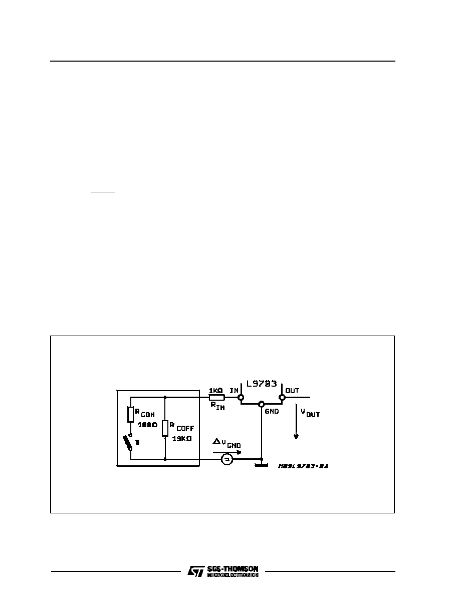
Figure 1 : Typical Application Diagram for the L9703 Circuit. The current flowing in the arrow direction is
assumed positive. The external capacitors C
IN
and C
OUT
represent the total wiring capacitance
at the corresponding pins.
APPLICATION CIRCUIT
L9703
4/9
FUNCTIONAL DESCRIPTION
The L9703 circuit monitors the status of the contacts
connected to ground and through this series exter-
nal resistors R
IN
to the contact sense input pins. The
contacts equivalent circuit is supposed to be as
shown in fig. 2.
The L9703 circuit compares the input current with
the current through the internal reference resistor.
The device is designed to work with an external input
series resistor of R
IN1-8
= 1k
. With this input resistor
the contact current, when the contact is closed and
the device activated (EN = LOW) is
V
S
- 2V
I
IN
=
1k
(1)
For this calculation the limit value of the V
S
to IN
saturation voltage of 2V was considered so that the
lowest limit value of I
IN
is calculated in (1).
The function of the circuit can be demonstrated with
the transfer characteristics, showing the output
status as a function of the input resistor R
I
, shown
in figure 3. The input resistor is a sum of the R
IN
and
the contact resistance R
CON
or R
COFF
, for the closed
contact :
R
I
= R
IN
+ R
CON,
(2)
and for the open contact :
R
I
= R
IN
+ R
COFF
.
(3)
The output goes HIGH when the input resistance in-
creases above5.3k
(typical value) and goes LOW,
when the input resistance decreases below 4k
(typical value). The limit values of R
I
= 1.8K
for
LOW and R
I
= 20k
for HIGH implies that a contact
with R
CON
= 100
(at I
IN
= 10mA) will be recognized
as ON = LOW and a contact with R
COFF
= 19k
will
be recognized as OFF = HIGH. These limits are
valid within the supply voltage range 6V
VS
16V
and
the
ground
potential
difference
of
VGND
= 0,1V.
The internal clamping diodes at the contact moni-
toring inputs, together with the external contacts se-
ries resistors R
IN
, allows the device to withstand
transientsat the contactconnection.The contactse-
ries resistor R
IN
limits the input current at the tran-
sient.
The dynamic behaviour of the circuit is defined by
the times t
do
and t
dTs
. When the contact is open, the
input capacitor C
IN
must be charged through the re-
sistor R
IN
. In this case the total delay time may also
be influenced by the time constant R
IN
C
IN
.
The delay time t
dTs
, when disabling the device, is de-
fined only by the internal circuitry. In both cases, an
external output capacitance less than 50pF is as-
sumed, the internal output capacitances of the
three-state buffers are less than 5pF.
Figure 2 : The Contact Sense Input Connection with the Contact Equivalent Circuit.
L9703
5/9
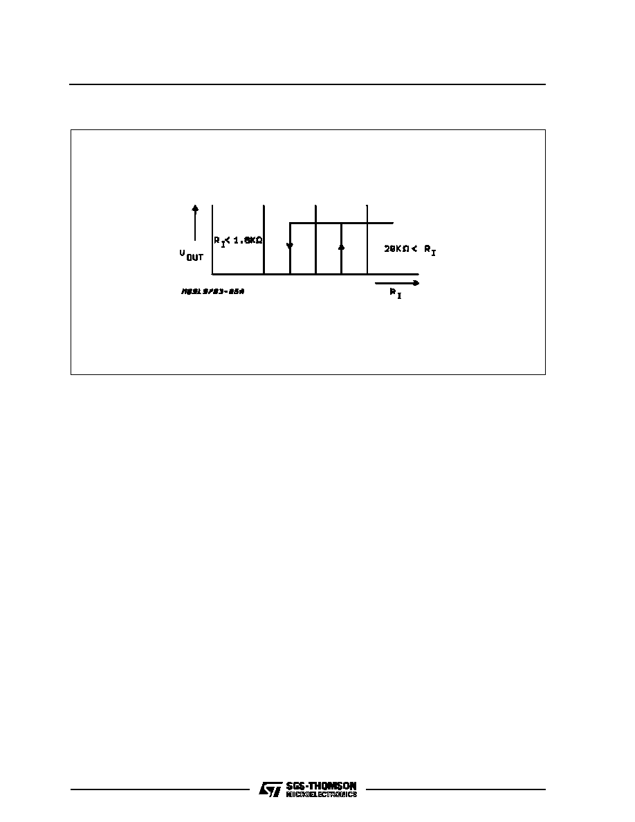
Figure 3 : The Output Voltage as a Function of the Input Resistance at the Corresponding Contact Sense
Input.
L9703
6/9
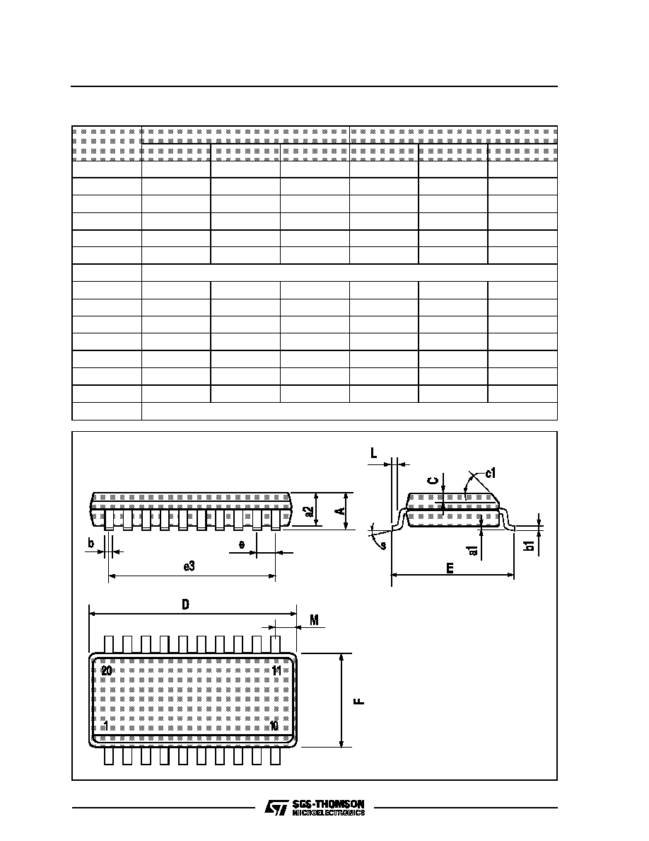
SO20 PACKAGE MECHANICAL DATA
DIM.
mm
inch
MIN.
TYP.
MAX.
MIN.
TYP.
MAX.
A
2.65
0.104
a1
0.1
0.3
0.004
0.012
a2
2.45
0.096
b
0.35
0.49
0.014
0.019
b1
0.23
0.32
0.009
0.013
C
0.5
0.020
c1
45 (typ.)
D
12.6
13.0
0.496
0.512
E
10
10.65
0.394
0.419
e
1.27
0.050
e3
11.43
0.450
F
7.4
7.6
0.291
0.299
L
0.5
1.27
0.020
0.050
M
0.75
0.030
S
8 (max.)
L9703
7/9
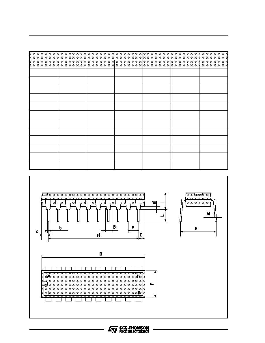
DIP20 PACKAGE MECHANICAL DATA
DIM.
mm
inch
MIN.
TYP.
MAX.
MIN.
TYP.
MAX.
a1
0.254
0.010
B
1.39
1.65
0.055
0.065
b
0.45
0.018
b1
0.25
0.010
D
25.4
1.000
E
8.5
0.335
e
2.54
0.100
e3
22.86
0.900
F
7.1
0.280
I
3.93
0.155
L
3.3
0.130
Z
1.34
0.053
L9703
8/9

Information furnished is believed to be accurate and reliable. However, SGS-THOMSON Microelectronics assumes no responsibility for
the consequences of use of such information nor for any infringement of patents or other rights of third parties which may result from its
use. No license is granted by implication or otherwise under any patent or patent rights of SGS-THOMSON Microelectronics. Specifica-
tions mentioned in this publication are subject to change without notice. This publication supersedes and replaces all information pre-
viously supplied. SGS-THOMSON Microelectronics products are not authorized for use as critical components in life support devices or
systems without express written approval of SGS-THOMSON Microelectronics.
©
1994 SGS-THOMSON Microelectronics - All Rights Reserved
SGS-THOMSON Microelectronics GROUP OF COMPANIES
Australia - Brazil - France - Germany - Hong Kong - Italy - Japan - Korea - Malaysia - Malta - Morocco - The Netherlands - Singapore -
Spain - Sweden - Switzerland - Taiwan - Thaliand - United Kingdom - U.S.A.
L9703
9/9