
LCDP1511D
Æ
September 1999 - Ed:2A
DUAL LINE PROGRAMMABLE TRANSIENT
VOLTAGE SUPPRESSOR FOR SLIC PROTECTION
SO8
Dual line programmable transient suppressor
Wide negative firing voltage range : V
MGL
= -80V
Low dynamic switching voltages : V
FP
and V
DGL
Low gate triggering current : I
GT
= 5mA max
Peak pulse current : I
PP
= 15 A (10/1000
µ
s)
Holding current : I
H
> 150 mA
FEATURES
The LCDP1511D is a dual line protector which pro-
tects subscriber line interface circuits (SLIC)
against transient overvoltages.
Positive overvoltages are clamped with diodes to-
wards GND, while negative overvoltages are sup-
pressed by thyristors connected to GND. The
breakdown voltage of the thyristors is determined
by the voltage applied to the gate, generally -V
bat
.
DESCRIPTION
Application Specific Discretes
A.S.D.
TM
COMPLIES WITH THE
FOLLOWING STANDARDS:
Peak Surge
Voltage
(V)
Voltage
Waveform
(
µ
s)
Current
Waveform
(
µ
s)
Admissible
Ipp
(A)
Necessary
Resistor
(
)
ITU-T K20
1000
10/700
5/310
25
-
VDE0433
2000
10/700
5/310
25
40
VDE0878
1500
1.2/50
1/20
40
-
IEC1000-4-5
level 2
level 2
10/700
1.2/50
5/310
8/20
25
25
-
-
FCC Part 68
1500
800
10/160
10/560
10/160
10/560
30
20
-
5
BELLCORE NWT-001089-CORE
2500
1000
2/10
10/1000
2/10
10/1000
70
15
25
45
TIP 1
RING 1
8
1
TIP 2
RING 2
5
4
GATE
GATE
2
3
GND
GND
7
6
FUNCTIONAL DIAGRAM
1/6

Symbol
Parameter
Value
Unit
Rth (j-a)
Junction to ambient
170
∞
C/W
THERMAL RESISTANCE
Symbol
Parameter
Value
Unit
I
PP
Peak pulse current (see note1)
10/1000
µ
s
5/310
µ
s
2/10
µ
s
15
25
70
A
I
FSM
Non repetitive surge peak on-state current
(see note2)
t
p
= 10ms
t
p
= 1s
5
3.5
A
V
MLG
V
MGL
Maximum voltage LINE/GND
Maximum voltage GATE/LINE
80
80
V
T
stg
Storage temperature range
- 55 to + 150
∞
C
T
L
Lead temperature for soldering during 10s
260
∞
C
ABSOLUTE MAXIMUM RATINGS (T
amb
= 25∞C).
100
50
% IPP
t
t
t
r
p
0
Note 1: Pulse waveform
10 / 1000
µ
s
tr = 10
µ
s
tp = 1000
µ
s
5 / 310
µ
s
tr = 5
µ
s
tp = 310
µ
s
2 / 10
µ
s
tr = 2
µ
s
tp = 10
µ
s
Note 2 : Maximum current flowing through the 4 wires together.
Symbol
Parameter
I
GT
Gate triggering current
I
H
Holding current
I
RM
Reverse leakage current LINE / GND
I
RG
Reverse leakage current GATE / LINE
V
RM
Reverse voltage LINE / GND
V
GT
Gate triggering voltage
V
F
Forward drop voltage LINE / GND
V
FP
Peak forward voltage
V
DGL
Dynamic switching voltage GATE / LINE
V
GATE
GATE / GND voltage
V
RG
Reverse voltage GATE / LINE
C
Capacitance LINE / GND
ELECTRICAL CHARACTERISTICS (T
amb
= 25∞C)
V
DGL
V
RM
V
R
I
PP
I
H
I
R
I
RM
V
F
LCDP1511D
2/6
Symbol
Test conditions
Max
Unit
V
F
Square pulse : t
p
= 500
µ
s I
F
= 1A
2
V
V
FP
(note 1)
10/700
µ
s
1.2/50
µ
s
2/10
µ
s
1kV
1.5kV
2.5kV
R
P
= 60
R
P
= 60
R
P
= 245
I
PP
= 10A
I
PP
= 15A
I
PP
= 10A
5
10
20
V
note 1 : see test circuit for VFP, RP is the protection resistor located on the line card
PARAMETERS RELATED TO THE DIODE LINE / GND (T
amb
= 25∞C)
Symbol
Test conditions
Max
Unit
I
RM
V
GATE / LINE
= -1V V
RM
= -75V
5
µ
A
C
V
R
= -3V F = 1MHz
V
R
= -48V F = 1MHz
200
100
pF
PARAMETERS RELATED TO LINE / GND (T
amb
= 25∞C)
Symbol
Test conditions
Min
Max
Unit
I
GT
V
GND / LINE
= -48V
5
mA
I
H
V
GATE
= -48V (see note 2)
150
mA
V
GT
at I
GT
2.5
V
I
RG
V
RG
= -75V
5
µ
A
V
DGL
V
GATE
= -48V (see note 3)
10/700
µ
s
1.2/50
µ
s
2/10
µ
s
1kV
1.5kV
2.5kV
R
P
= 60
R
P
= 60
R
P
=245
I
PP
= 10A
I
PP
= 15A
I
PP
= 10A
7
15
20
V
note 2 : see functional holding current test circuit
note 3 : See test circuit for VDGL
The oscillations with a time duration lower than 50ns are not taken into account
PARAMETERS RELATED TO THE PROTECTION THYRISTOR (T
amb
= 25∞C)
0.01
0.10
1.00
10.00
100.00
1000.00
0
1
2
3
4
5
6
7
t(s)
ITSM(A)
F=50Hz
Tj initial=25∞C
Fig. 1: Surge peak current versus overload duration.
-40
-20
0
20
40
60
80
100
120
0.0
0.2
0.4
0.6
0.8
1.0
1.2
1.4
1.6
1.8
2.0
Tj(∞C)
IH[Tj] / IH[Tj=25∞C]
Fig. 2: Relative variation of holding current versus
junction temperature.
LCDP1511D
3/6
Pulse (
µ
s)
V
p
C
1
C
2
L
R
1
R
2
R
3
R
4
I
PP
R
p
t
r
t
p
(V)
(
µ
F)
(nF)
(
µ
H)
(
)
(
)
(
)
(
)
(A)
(
)
10
700
1000
20
200
0
50
15
25
25
10
60
1.2
50
1500
1
33
0
76
13
25
25
15
60
2
10
2500
10
0
1.1
1.3
0
3
3
10
245
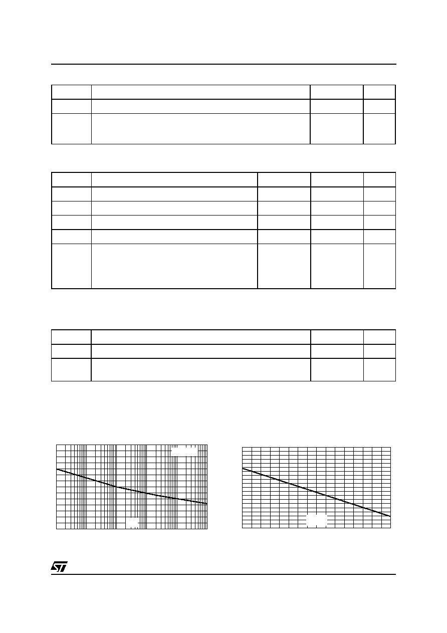
TEST CIRCUIT FOR V
FP
AND V
DGL
PARAMETERS
This is a GO-NO GO test which allows to confirm the holding current (I
H
) level in a functional test circuit.
TEST PROCEDURE :
- Adjust the current level at the I
H
value by short circuiting the D.U.T.
- Fire the D.U.T. with a surge current : I
PP
= 15A, 10/1000
µ
s.
- The D.U.T. will come back to the off-state within a duration of 50ms max.
C
C
R
R
TIP
R ING
G ND
V
P
4
3
2
R
2
R
1
(V is defined in unload condition)
P
L
1
R
- V
P
V
BAT
- 48 V
=
Surge generator
D.U.T.
FUNCTIONAL HOLDING CURRENT (I
H
) TEST CIRCUIT : GO-NO GO TEST
LCDP1511D
4/6

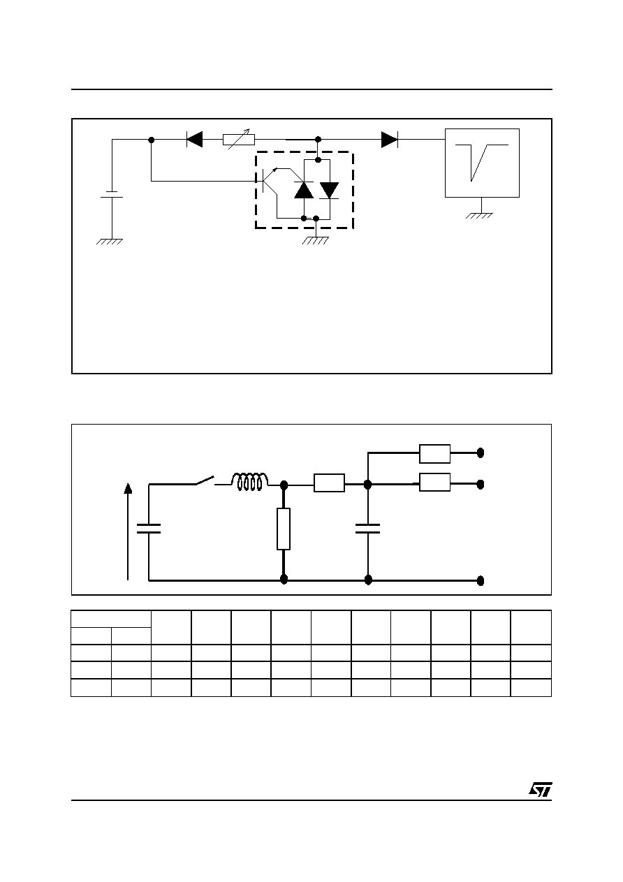
APPLICATION CIRCUIT: PABX line protection
APPLICATION CIRCUIT: Line Card protection
LCDP1511D
SLIC
-Vbat
SLIC
-Vbat
PTC or Fuse
PTC or Fuse
R
P
R
P
Line 1
CLP30-200B1
PTC or Fuse
PTC or Fuse
R
P
R
P
Line 2
CLP30-200B1
Ring
relay
1
Ring
relay
2
LCDP1511D
SLIC
-Vbat
SLIC
-Vbat
PTC or Fuse
PTC or Fuse
R
P
P
R
R
R
R
R
R
P
P
P
Line 1
Ring relay
Ring
relay
1
protection
PTC or Fuse
PTC or Fuse
Line 2
Ring relay
protection
Ring
relay
2
LCDP1511D
5/6