1/7
Application Specific Discretes
A.S.D.TM
LCP1511D
PROGRAMMABLE TRANSIENT VOLTAGE
SUPPRESSOR FOR SLIC PROTECTION
Æ
n
DUAL PROGRAMMABLE TRANSIENT SUP-
PRESSOR.
n
WIDE NEGATIVE FIRING VOLTAGE RANGE :
V
MGL
= -80V max.
n
LOW DYNAMIC SWITCHING VOLTAGES :
V
FP
and V
DGL
.
n
LOW GATE TRIGGERING CURRENT :
I
GT
= 5mA max.
n
PEAK PULSE CURRENT :
I
PP
= 30A for 10/1000
µ
s surge.
n
HOLDING CURRENT :
I
H
= 150mA.
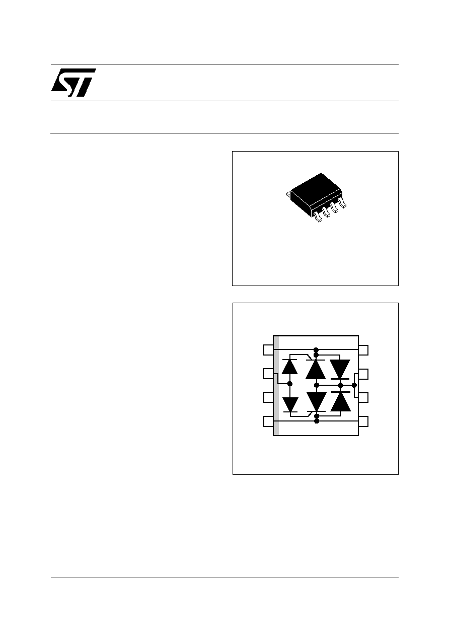
FEATURES
SO-8
This device has been especially designed to pro-
tect subscriber line card interfaces (SLIC) against
transient overvoltages.
Positive overloads are clipped with 2 diodes. Neg-
ative surges are suppressed by 2 thyristors, their
breakdown voltage being referenced to
-V
BAT
through the gate.
This component presents a very low gate
trigge-ring current (I
GT
) in order to reduce the cur-
rent consumption on printed circuit board during
the firing phase.
A particular attention has been given to the internal
wire bonding. The "4-point" configuration ensures
reliable protection, eliminating the overvoltage in-
troduced by the parasitic inductances of the wiring
(Ldi/dt), especially for very fast transients.
DESCRIPTION
October 2003 - Ed: 4
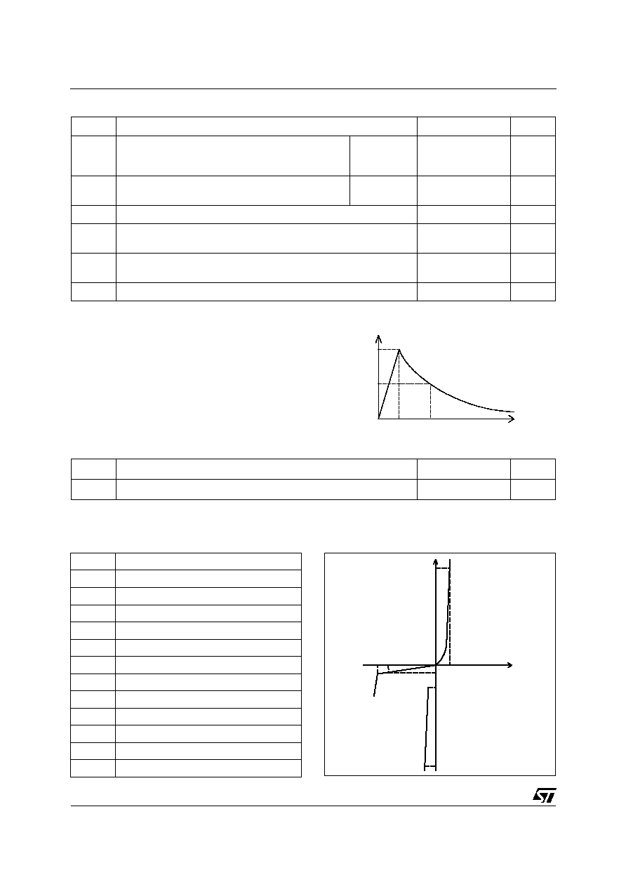
SCHEMATIC DIAGRAM
GND
GND
TIP
TIP
RING
RING
1
2
3
4
5
6
7
8
GATE
NC
CCITT K20 :
10/700
µ
s
1kV
5/310
µ
s
25A
VDE 0433 :
10/700
µ
s
2kV
5/310
µ
s
38A (*)
VDE 0878 :
1.2/50
µ
s
1.5kV
1/20
µ
s
40A
I3124 :
0.5/700
µ
s
1kV
0.2/310
µ
s
25A
FCC part 68 :
2/10
µ
s
2.5kV
2/10
µ
s
170A (*)
BELLCORE
TR-NWT-001089 : 2/10
µ
s
2.5kV
2/10
µ
s
170A (*)
(*) with series resistors or PTC.
COMPLIES WITH THE FOLLOWING STANDARDS
TM: ASD is trademarks of STMicroelectronics.
LCP1511D
2/7
Symbol
Parameter
Value
Unit
I
PP
Peak pulse current
(see note 1)
10/1000
µ
s
5/310
µ
s
2/10
µ
s
30
38
170
A
I
TSM
Non repetitive surge peak on-state current
(F = 50Hz)
t
p
= 10ms
t = 1s
8
3.5
A
I
GSM
Maximum gate current (half sine wave tp = 10ms)
2
A
V
MLG
V
MGL
Maximum voltage LINE / GROUND
Maximum voltage GATE / LINE
-100
-80
V
T
stg
T
j
Storage temperature range
Maximum junction temperature
- 55 to + 150
150
∞
C
T
L
Maximum lead temperature for soldering during 10s
260
∞C
ABSOLUTE MAXIMUM RATINGS (T
amb
= 25 ∞C)
Note 1 : Pulse waveform :
10/1000
µ
s
tr=10
µ
s
tp=1000
µ
s
5/310
µ
s
tr=5
µ
s
tp=310
µ
s
2/10
µ
s
tr=2
µ
s
tp=10
µ
s
Symbol
Parameter
Value
Unit
R
th (j-a)
Junction to ambient
170
∞
C/W
THERMAL RESISTANCE
Symbol
Parameter
I
GT
Gate triggering current
I
H
Holding current
I
RM
Reverse leakage current LINE/GND
I
RG
Reverse leakage current GATE/LINE
V
RM
Reverse voltage LINE/GND
V
F
Forward drop voltage LINE/GND
V
GT
Gate triggering voltage
V
FP
Peak forward voltage LINE/GND
V
DGL
Dynamic switching voltage GATE/LINE
V
GATE
GATE/GND voltage
V
LG
LINE/GND voltage
C
Off-state capacitance LINE/GND
ELECTRICAL CHARACTERISTICS (T
amb
= 25∞C)
I
I
H
I
PP
V
GATE
V
F
I
RM
V
LG
V
RM
I
F
100
50
% I
PP
t
t
r
p
0
t
LCP1511D
3/7
APPLICATION NOTE
Symbol
Test conditions
Maximum
Unit
V
F
I
F
=5A
t
p
=500
µ
s
3
V
V
FP
10/700
µ
s
1.5kV
R
p
=10
1.2/50
µ
s
1.5kV
R
p
=10
(see note 1)
2/10
µ
s
2.5kV
R
p
=62
5
7
12
V
Note 1 : See test circuit 2 for V
FP
; R
p
is the protection resistor located on the line card.
1 - PARAMETERS RELATED TO THE DIODE LINE/GND (T
amb
= 25 ∞C)
Sym-
bol
Test conditions
Min.
Max.
Unit
I
GT
V
GND/LINE
= -48V
0.2
5
mA
I
H
V
GATE
=-48V (see note 2)
150
mA
V
GT
at I
GT
2.5
V
I
RG
T
c
=25∞C
V
RG
=-75V
T
c
=70∞C
V
RG
=-75V
5
50
µ
A
V
DGL
VGATE= -48V (see note 3)
10/700
µ
s
1.5kV
Rp=10
I
PP
=30A
1.2/50
µ
s
1.5kV
Rp=10
I
PP
=30A
2/10
µ
s
2.5kV
Rp=62
I
PP
=38A
10
20
25
V
Note 2 :
See the functional holding current (I
H
) test circuit 2.
2 - PARAMETERS RELATED TO THE PROTECTION THYRISTOR (T
amb
= 25∞C)
Sym-
bol
Test conditions
Maximum
Unit
I
RM
T
c
=25∞C
V
GATE/LINE
= -1V
V
RM
=-75V
T
c
=70∞C
V
GATE/LINE
= -1V
V
RM
=-75V
5
50
µ
A
3 - PARAMETERS RELATED TO DIODE AND PROTECTION THYRISTOR (T
amb
= 25 ∞C)
1
2
3
4
8
7
6
5
IN
IN
OUT
OUT
TIP
RING
GND
TIP
RING
GATE
NC
In order to take advantage of the "4 point" structure
of the LCP, the TIP and RING lines go across the
device. In such case, the device will eliminate the
overvoltages generated by the parasitic induc-
tances of the wiring (Ldi/dt), especially for very fast
transients.
LCP1511D
4/7
R
P
V
BAT
48V
=
-
D.U.T.
Surge
generator
This is a GO-NO GO test which allows to confirm the holding current (I
H
) level in a functional test circuit.
TEST PROCEDURE :
- Adjust the current level at the I
H
value by short circuiting the D.U.T.
- Fire the D.U.T. with a surge current : I
PP
= 10A, 10/1000
µ
s.
- The D.U.T. will come back to the off-state within a duration of 50ms max.
C
C
R
R
TIP
R ING
G ND
V
P
4
3
2
R
2
R
1
(V is defined in unload condition)
P
L
1
Pulse (
µ
s)
V
p
C
1
C
2
L
R
1
R
2
R
3
R
4
I
PP
R
p
t
r
t
p
(V)
(
µ
F)
(nF)
(
µ
H)
(
)
(
)
(
)
(
)
(A)
(
)
10
700
1500
20
200
0
50
15
25
25
30
10
1.2
50
1500
1
33
0
76
13
25
25
30
10
2
10
2500
10
0
1.1
1.3
0
3
3
38
62
FUNCTIONAL HOLDING CURRENT (I
H
) TEST CIRCUIT 1 : GO-NO GO TEST
TEST CIRCUIT 2 FOR V
FP
AND V
DGL
PARAMETERS
LCP1511D
5/7
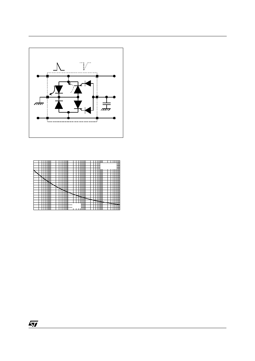
FUNCTIONAL DESCRIPTION
LINE A
LINE B
D
D
P
P
TIP
RING
- V
BAT
1
1
2
2
C
LINE A PROTECTION :
≠ For positive surges versus GND, the diode D1
will conduct.
≠ For negative surges versus GND, the protection
device P1 will trigger at a voltage fixed by the
-V
BAT
reference.
LINE B PROTECTION :
≠ For surges on line B, the operating mode is the
same, D2 or P2 is activated.
It is recommended to add a capacitor (C=220nF)
close to the gate of the LCP, in order to speed up
the triggering.
1E-2
1E-1
1E+0
1E+1
1E+2
1E+3
0
1
2
3
4
5
6
7
8
9
10
I
(A)
TSM
F=50Hz
Tj initial=25∞C
t(s)
Surge peak current versus overload duration.