1/20
October 2003
s
TYPICAL DROPOUT 1.3V AT 1.5A
s
THREE TERMINAL ADJUSTABLE OR FIXED
OUTPUT VOLTAGE 1.2V, 1.5V, 1.8V, 2.5V,
2.85V, 3.3V, 3.6V, 5V, 8V, 9V, 12V.
s
GUARANTEED OUTPUT CURRENT UP TO
1.5A
s
OUPUT TOLERANCE
±
1% AT 25∞C AND
±
2% IN FULL TEMPERATURE RANGE
s
INTERNAL POWER AND THERMAL LIMIT
s
WIDE OPERATING TEMPERATURE RANGE
-40∞C TO 125∞C
s
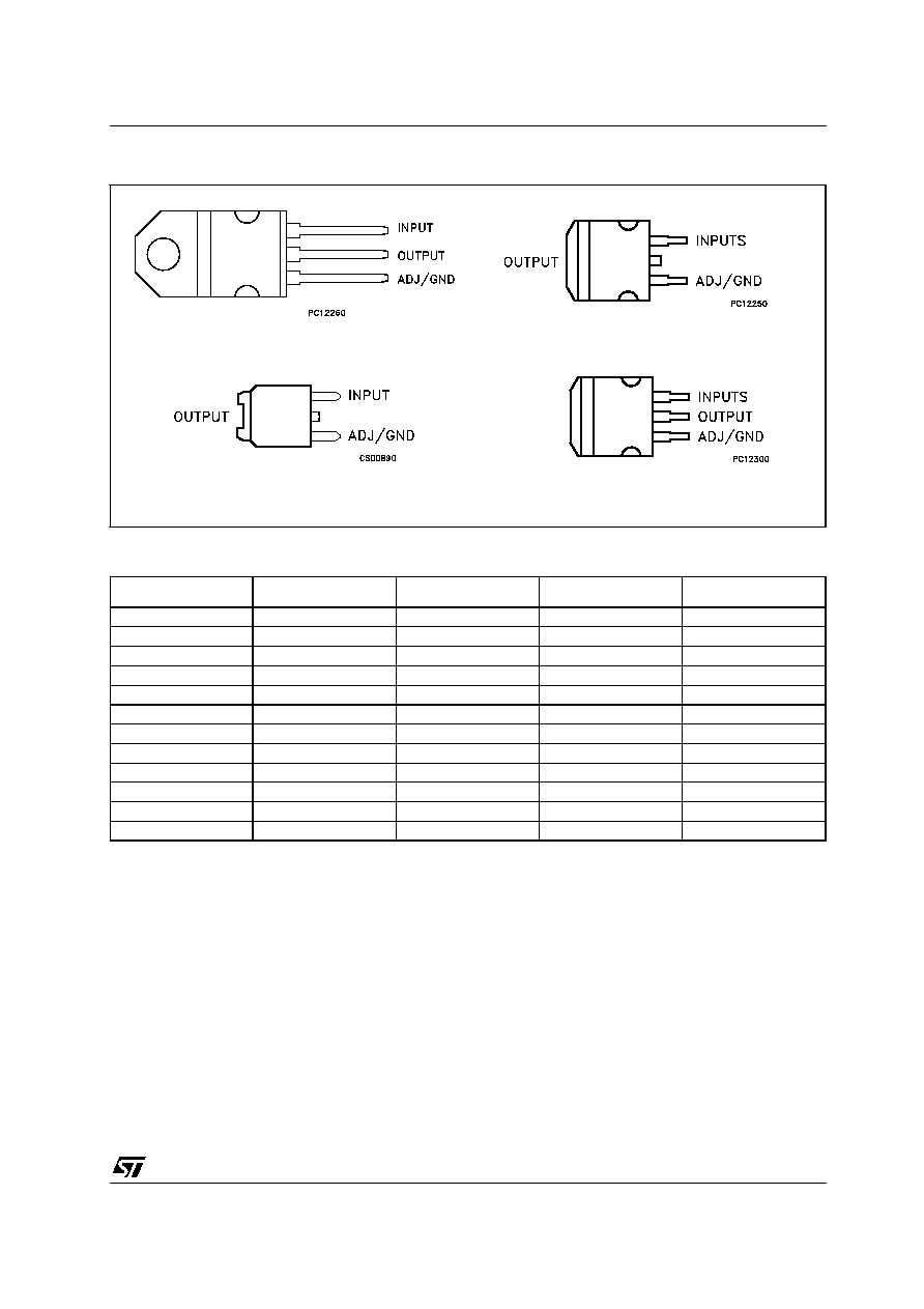
PACKAGE AVAILABLE : TO-220, D
2
PAK,
D
2
PAK/A, DPAK
s
PINOUT COMPATIBILITY WITH STANDARD
ADJUSTABLE VREG
DESCRIPTION
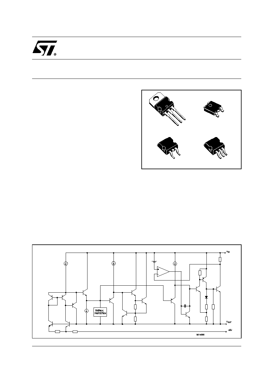
The LD1086 is a LOW DROP Voltage Regulator
able to provide up to 1.5A of Output Current.
Dropout is guaranteed at a maximum of 1.2V at
the maximum output current, decreasing at lower
loads. The LD1086 is pin to pin compatible with
the older 3-terminal adjustable regulators, but has
better performances in term of drop and output
tolerance .
A 2.85V output version is suitable for SCSI-2
active termination. Unlike PNP regulators, where
a part of the output current is wasted as quiescent
current, the LD1086 quiescent current flows into
the load, so increase efficiency. Only a 10µF
minimum capacitor is need for stability. The
device is supplied in TO-220, D
2
PAK, D
2
PAK/A
and DPAK. On chip trimming allows the regulator
to reach a very tight output voltage tolerance,
within ±1% at 25∞C.
LD1086
SERIES
1.5A LOW DROP POSITIVE VOLTAGE
REGULATOR ADJUSTABLE AND FIXED
SCHEMATIC DIAGRAM
TO-220
DPAK
D
2
PAK
D
2
PAK/A
LD1086 SERIES
2/20
ABSOLUTE MAXIMUM RATINGS
Absolute Maximum Ratings are those values beyond which damage to the device may occur. Functional operation under these condition is
not implied.
THERMAL DATA
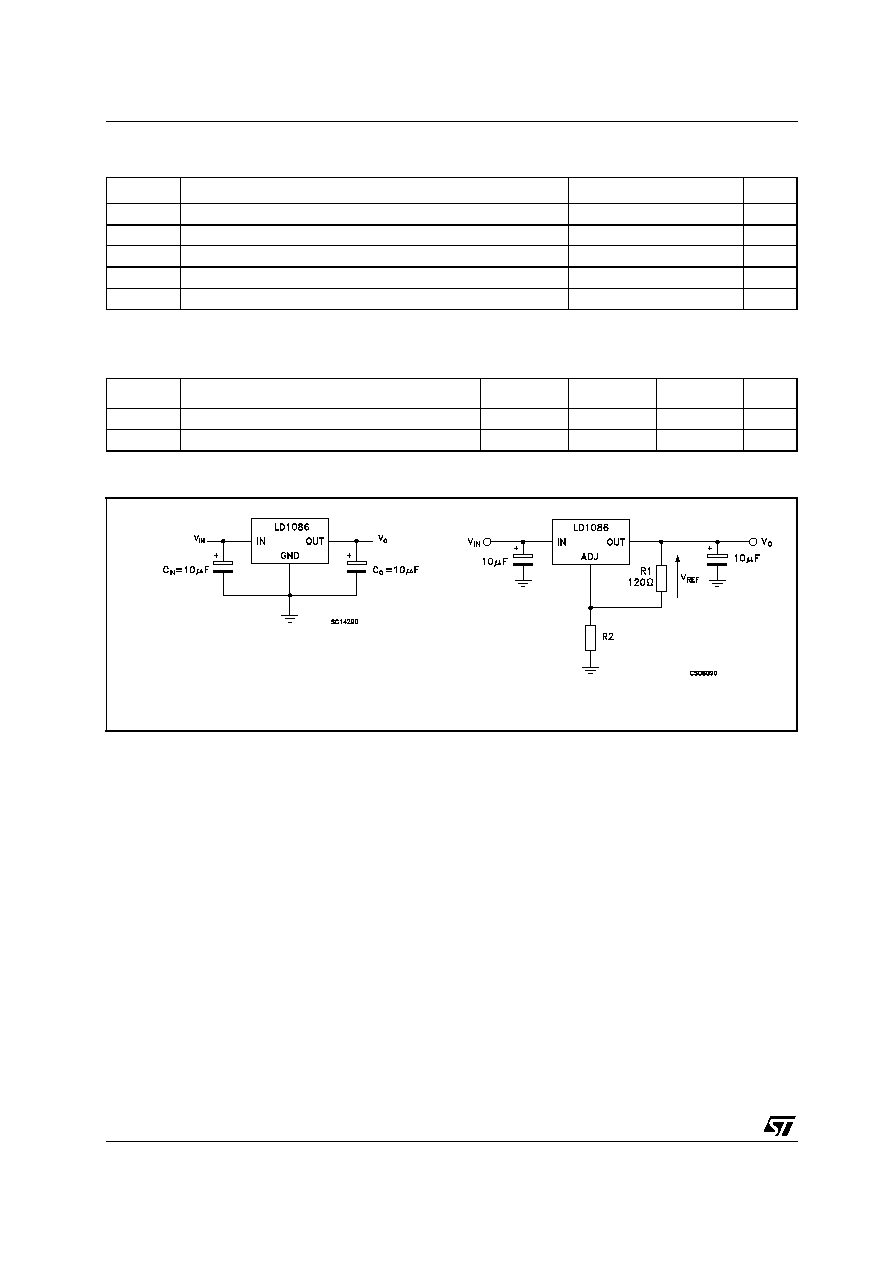
APPLICATION CIRCUITS
Symbol
Parameter≤
Value
Unit
V
I
DC Input Voltage
30
V
I
O
Output Current
Internally Limited
mA
P
D
Power Dissipation
Internally Limited
mW
T
stg
Storage Temperature Range
-55 to +150
∞C
T
op
Operating Junction Temperature Range
-40 to +125
∞C
Symbol
Parameter
TO-220
D
2
PAK
DPAK
Unit
R
thj-case
Thermal Resistance Junction-case
3
3
8
∞C/W
R
thj-amb
Thermal Resistance Junction-ambient
50
62.5
∞C/W
R
2
V
O
= V
REF
(1 +
)
R
1
LD1086 SERIES
4/20
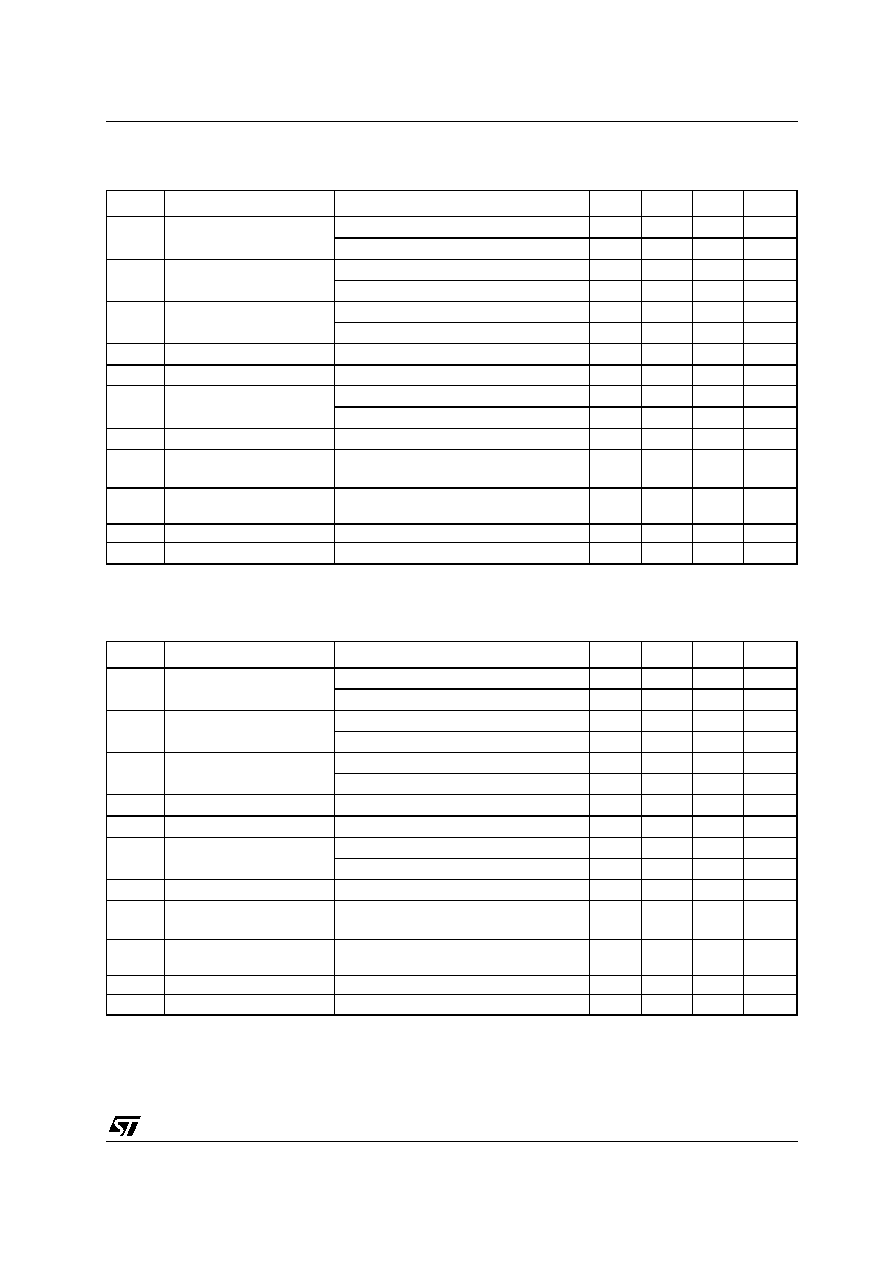
ELECTRICAL CHARACTERISTICS OF LD1086#12 (V
I
=4.5V, C
I
= C
O
=10
µ
F, T
A
= -40 to 125∞C, unless
otherwise specified.)
NOTE 1: See short-circuit current curve for available output current at fixed dropout.
ELECTRICAL CHARACTERISTICS OF LD1086#15 (V
I
=4.5V, C
I
= C
O
=10
µ
F, T
A
= -40 to 125∞C, unless
otherwise specified.)
NOTE 1: See short-circuit current curve for available output current at fixed dropout.
Symbol
Parameter
Test Conditions
Min.
Typ.
Max.
Unit
V
O
Output Voltage (note 1)
I
O
= 0 mA
T
J
= 25∞C
1.485
1.5
1.515
V
I
O
= 0 to 1.5A
V
I
= 3.4 to 30V
1.47
1.5
1.53
V
V
O
Line Regulation
I
O
= 0 mA
V
I
= 3.1 to 18V
T
J
= 25∞C
0.2
4
mV
I
O
= 0 mA
V
I
= 3.1 to 15V
0.4
4
mV
V
O
Load Regulation
I
O
= 0 to 1.5A
T
J
= 25∞C
0.5
8
mV
I
O
= 0 to 1.5A
1
16
V
V
d
Dropout Voltage
I
O
= 1.5A
1.3
1.5
V
I
q
Quiescent Current
V
I
30V
5
10
mA
I
sc
Short Circuit Current
V
I
- V
O
= 5V
1.5
2
A
V
I
- V
O
= 25V
0.05
0.02
A
Termal Regulation
T
A
= 25∞C, 30ms pulse
0.01
0.04
%/W
SVR
Supply Voltage Rejection
f = 120 Hz,
C
O
= 25
µ
F, I
O
= 1.5A
V
I
= 6.5
±
3V
60
82
dB
eN
RMS Output Noise Voltage
(% of V
O
)
T
A
= 25∞C
f =10Hz to 10KHz
0.003
%
S
Temperature Stability
0.5
%
S
Long Term Stability
T
A
= 125∞C
1000Hrs
0.5
%
LD1086 SERIES
5/20
ELECTRICAL CHARACTERISTICS OF LD1086#18 (V
I
=4.8V, C
I
= C
O
=10
µ
F, T
A
= -40 to 125∞C, unless
otherwise specified.)
NOTE 1: See short-circuit current curve for available output current at fixed dropout.
ELECTRICAL CHARACTERISTICS OF LD1086#25 (V
I
=5.5V, C
I
= C
O
=10
µ
F, T
A
= -40 to 125∞C, unless
otherwise specified.)
NOTE 1: See short-circuit current curve for available output current at fixed dropout.
Symbol
Parameter
Test Conditions
Min.
Typ.
Max.
Unit
V
O
Output Voltage (note 1)
I
O
= 0 mA
T
J
= 25∞C
1.782
1.8
1.818
V
I
O
= 0 to 1.5A
V
I
= 3.4 to 30V
1.764
1.8
1.836
V
V
O
Line Regulation
I
O
= 0 mA
V
I
= 3.4 to 18V
T
J
= 25∞C
0.2
4
mV
I
O
= 0 mA
V
I
= 3.4 to 15V
0.4
4
mV
V
O
Load Regulation
I
O
= 0 to 1.5A
T
J
= 25∞C
0.5
8
mV
I
O
= 0 to 1.5A
1
16
V
V
d
Dropout Voltage
I
O
= 1.5A
1.3
1.5
V
I
q
Quiescent Current
V
I
30V
5
10
mA
I
sc
Short Circuit Current
V
I
- V
O
= 5V
1.5
2
A
V
I
- V
O
= 25V
0.05
0.02
A
Termal Regulation
T
A
= 25∞C, 30ms pulse
0.01
0.04
%/W
SVR
Supply Voltage Rejection
f = 120 Hz,
C
O
= 25
µ
F, I
O
= 1.5A
V
I
= 6.8
±
3V
60
82
dB
eN
RMS Output Noise Voltage
(% of V
O
)
T
A
= 25∞C
f =10Hz to 10KHz
0.003
%
S
Temperature Stability
0.5
%
S
Long Term Stability
T
A
= 125∞C
1000Hrs
0.5
%
Symbol
Parameter
Test Conditions
Min.
Typ.
Max.
Unit
V
O
Output Voltage (note 1)
I
O
= 0 mA
T
J
= 25∞C
2.475
2.5
2.525
V
I
O
= 0 to 1.5A
V
I
= 4.1 to 30V
2.45
2.5
2.55
V
V
O
Line Regulation
I
O
= 0 mA
V
I
= 4.1 to 18V
T
J
= 25∞C
0.2
4
mV
I
O
= 0 mA
V
I
= 4.1 to 18V
0.4
4
mV
V
O
Load Regulation
I
O
= 0 to 1.5A
T
J
= 25∞C
0.5
8
mV
I
O
= 0 to 1.5A
1
16
V
V
d
Dropout Voltage
I
O
= 1.5A
1.3
1.5
V
I
q
Quiescent Current
V
I
30V
5
10
mA
I
sc
Short Circuit Current
V
I
- V
O
= 5V
1.5
2
A
V
I
- V
O
= 25V
0.05
0.2
A
Termal Regulation
T
A
= 25∞C, 30ms pulse
0.008
0.04
%/W
SVR
Supply Voltage Rejection
f = 120 Hz,
C
O
= 25
µ
F, I
O
= 1.5A
V
I
= 7.5
±
3V
60
81
dB
eN
RMS Output Noise Voltage
(% of V
O
)
T
A
= 25∞C
f =10Hz to 10KHz
0.003
%
S
Temperature Stability
0.5
%
S
Long Term Stability
T
A
= 125∞C
1000Hrs
0.5
%