1/16
October 2003
s
LOW DROPOUT VOLTAGE
(1.15V TYP. @ I
OUT
= 1A, 25∞C)
s
VERY LOW QUIESCENT CURRENT
(5 mA TYP. @ 25∞C)
s
OUTPUT CURRENT UP TO 1A
s
FIXED OUTPUT VOLTAGE OF: 1.8V, 2.5V,
2.85V, 3.3V, 5.0V
s
ADJUSTABLE VERSION AVAILABILITY
(V
rel
= 1.25V)
s
INTERNAL CURRENT AND THERMAL LIMIT
s
ONLY 10 µF FOR STABILITY
s
AVAILABLE IN ± 2% (AT 25∞C) AND 4% IN
FULL TEMPERATURE RANGE
s
HIGH SUPPLY VOLTAGE REJECTION:
(80dB TYP. AT 25∞C)
s
TEMPERATURE RANGE: 0∞C TO 125∞C
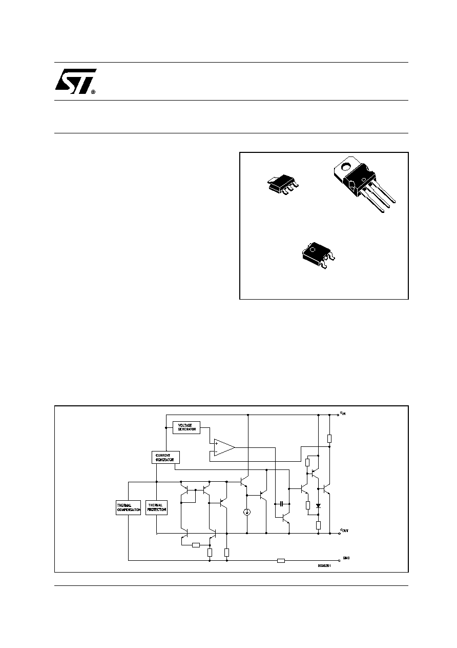
DESCRIPTION
The LD1117A is a LOW DROP Voltage Regulator
able to provide up to 1A of Output Current,
available even in adjustable version (Vref=1.25V).
Concerning
fixed
versions,
are
offered
the
following Output Voltages: 1.8V, 2.5V, 2.85V,
3.3V and 5.0V. The 2.85V type is ideal for SCSI-2
lines active termination. The device is supplied in:
SOT-223, DPAK and TO-220. The surface mount
packages optimize the thermal characteristics
even offering a relevant space saving effect. High
efficiency is assured by NPN pass transistor. Only
a very common 10µF minimum capacitor is
needed for stability. Only chip trimming allows the
regulator to reach a very tight output voltage
tolerance, within ± 2% at 25 ∞C.
LD1117A
SERIES
LOW DROP FIXED AND ADJUSTABLE
POSITIVE VOLTAGE REGULATORS
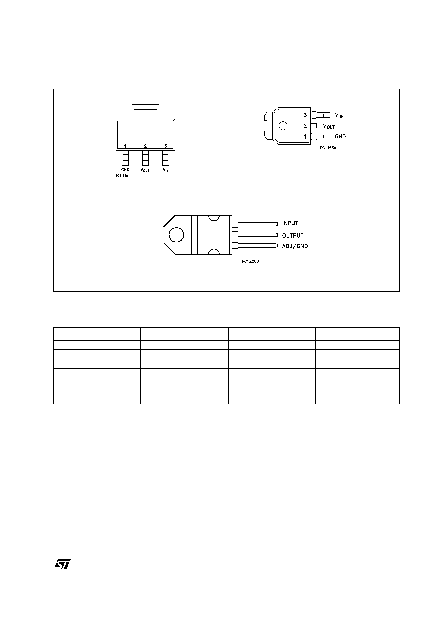
BLOCK DIAGRAM
SOT-223
DPAK
TO-220
LD1117A SERIES
2/16
ABSOLUTE MAXIMUM RATINGS
Absolute Maximum Ratings are those values beyond which damage to the device may occur. Functional operation under these condition is
not implied. Over the above suggested Max Power Dissipation a Short Circuit could definitively damage the device.
THERMAL DATA
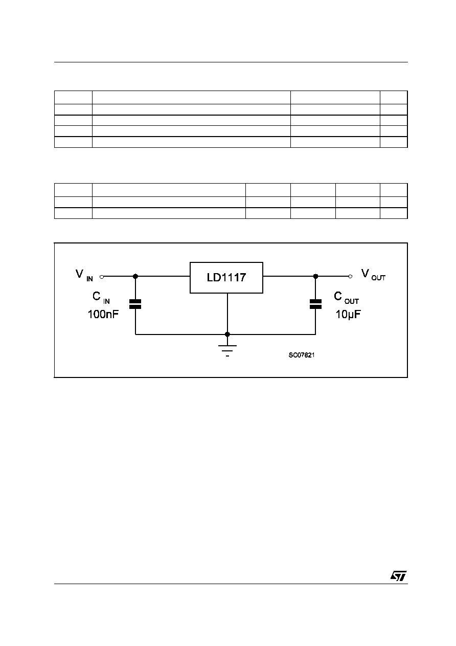
APPLICATION CIRCUIT (FOR OTHER FIXED OUTPUT VOLTAGES)
Symbol
Parameter≤
Value
Unit
V
IN
DC Input Voltage
10
V
P
tot
Power Dissipation
12
W
T
stg
Storage Temperature Range
-40 to +150
∞C
T
op
Operating Junction Temperature Range
0 to +125
∞C
Symbol
Parameter
TO-220
SOT-223
DPAK
Unit
R
thj-case
Thermal Resistance Junction-case
3
15
8
∞C/W
R
thj-amb
Thermal Resistance Junction-ambient
50
∞C/W
LD1117A SERIES
4/16
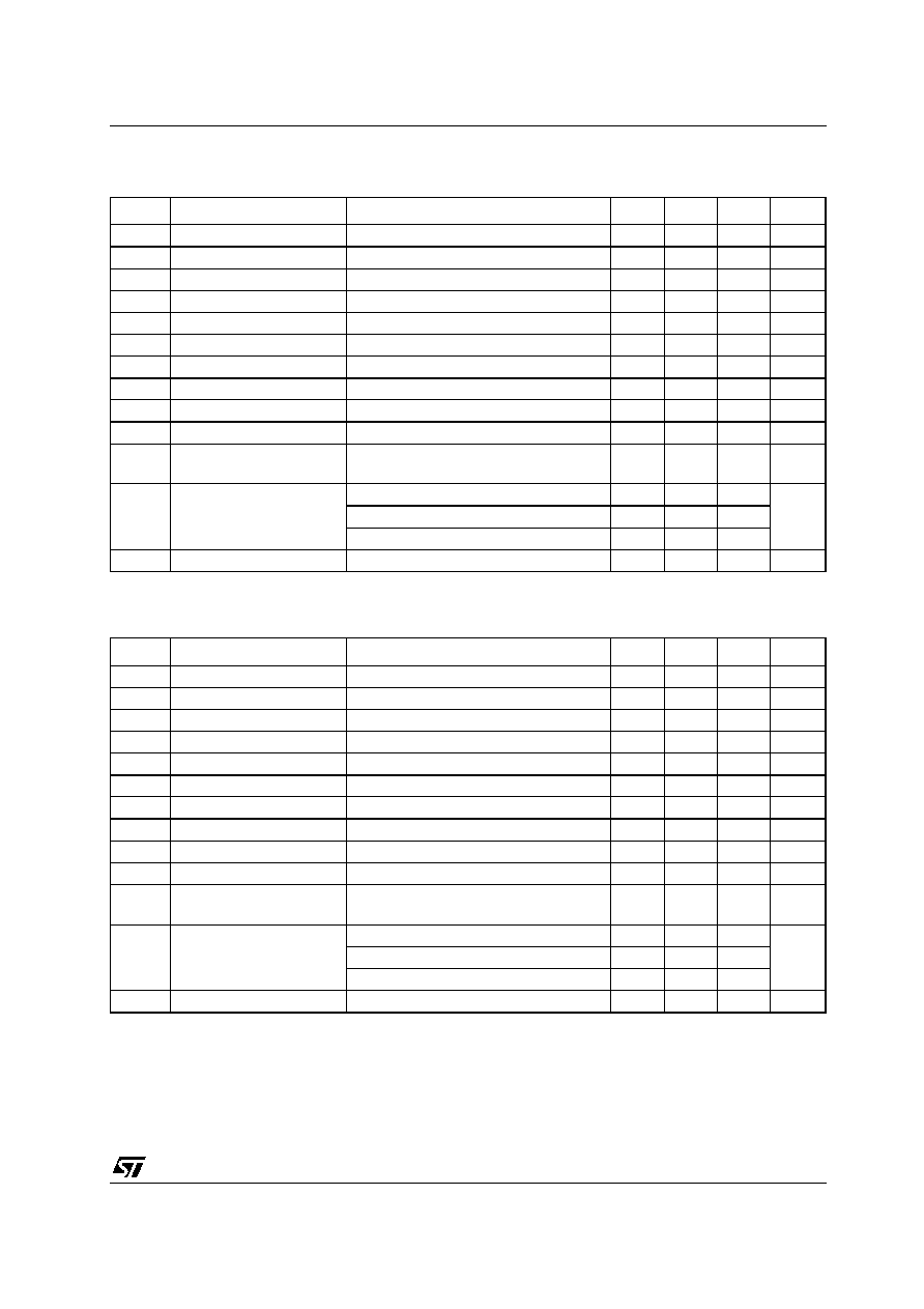
ELECTRICAL CHARACTERISTICS OF LD1117A#18 (refer to the test circuits, T
J
= 0 to 125∞C,
C
O
= 10 µF, C
I
= 10 µF unless otherwise specified)
ELECTRICAL CHARACTERISTICS OF LD1117A#25 (refer to the test circuits, T
J
= 0 to 125∞C,
C
O
= 10 µF, C
I
= 10 µF unless otherwise specified)
Symbol
Parameter
Test Conditions
Min.
Typ.
Max.
Unit
V
O
Output Voltage
V
I
= 3.8 V
I
O
= 10 mA
T
J
= 25∞C
1.764
1.8
1.836
V
V
O
Output Voltage
I
O
= 0 to 1 A
V
I
= 3.3 to 8 V
1.728
1.872
V
V
O
Line Regulation
V
I
= 3.3 to 8 V
I
O
= 0 mA
1
6
mV
V
O
Load Regulation
V
I
= 3.3 V
I
O
= 0 to 1 A
1
10
mV
V
O
Temperature Stability
0.5
%
V
O
Long Term Stability
1000 hrs, T
J
= 125∞C
0.3
%
V
I
Operating Input Voltage
I
O
= 100 mA
10
V
I
d
Quiescent Current
V
I
8 V
I
O
= 0 mA
5
10
mA
I
O
Output Current
V
I
- V
O
= 5 V T
J
= 25∞C
1000
mA
eN
Output Noise Voltage
B =10Hz to 10KHz T
J
= 25∞C
100
µ
V
SVR
Supply Voltage Rejection
I
O
= 40 mA
f = 120Hz
V
I
- V
O
= 3 V V
ripple
= 1 V
PP
60
80
dB
V
D
Dropout Voltage
I
O
= 100 mA
1
1.10
V
I
O
= 500 mA
1.05
1.15
I
O
= 1 A
1.15
1.30
V
O(pwr)
Thermal Regulation
T
a
= 25∞C
30ms Pulse
0.08
0.2
%/W
Symbol
Parameter
Test Conditions
Min.
Typ.
Max.
Unit
V
O
Output Voltage
V
I
= 4.5 V
I
O
= 10 mA
T
J
= 25∞C
2.45
2.5
2.55
V
V
O
Output Voltage
I
O
= 0 to 1 A
V
I
= 3.9 to 8 V
2.4
2.6
V
V
O
Line Regulation
V
I
= 3.9 to 8 V
I
O
= 0 mA
1
6
mV
V
O
Load Regulation
V
I
= 3.9 V
I
O
= 0 to 1 A
1
10
mV
V
O
Temperature Stability
0.5
%
V
O
Long Term Stability
1000 hrs, T
J
= 125∞C
0.3
%
V
I
Operating Input Voltage
I
O
= 100 mA
10
V
I
d
Quiescent Current
V
I
10 V
I
O
= 0 mA
5
10
mA
I
O
Output Current
V
I
- V
O
= 5 V T
J
= 25∞C
1000
1200
mA
eN
Output Noise Voltage
B =10Hz to 10KHz T
J
= 25∞C
100
µ
V
SVR
Supply Voltage Rejection
I
O
= 40 mA
f = 120Hz
V
I
- V
O
= 3 V V
ripple
= 1 V
PP
60
80
dB
V
D
Dropout Voltage
I
O
= 100 mA
1
1.10
V
I
O
= 500 mA
1.05
1.15
I
O
= 1 A
1.15
1.30
V
O(pwr)
Thermal Regulation
T
a
= 25∞C
30ms Pulse
0.08
0.2
%/W
LD1117A SERIES
5/16
ELECTRICAL CHARACTERISTICS OF LD1117A#28 (refer to the test circuits, T
J
= 0 to 125∞C,
C
O
= 10 µF, C
I
= 10 µF unless otherwise specified)
ELECTRICAL CHARACTERISTICS OF LD1117A#33 (refer to the test circuits, T
J
= 0 to 125∞C,
C
O
= 10 µF, C
I
= 10 µF unless otherwise specified)
Symbol
Parameter
Test Conditions
Min.
Typ.
Max.
Unit
V
O
Output Voltage
V
I
= 4.85 V
I
O
= 10 mA
T
J
= 25∞C
2.793
2.85
2.907
V
V
O
Output Voltage
I
O
= 0 to 1 A
V
I
= 4.25 to 10 V
2.736
2.964
V
V
O
Line Regulation
V
I
= 4.25 to 8 V
I
O
= 0 mA
1
6
mV
V
O
Load Regulation
V
I
= 4.25 V
I
O
= 0 to 1 A
1
10
mV
V
O
Temperature Stability
0.5
%
V
O
Long Term Stability
1000 hrs, T
J
= 125∞C
0.3
%
V
I
Operating Input Voltage
I
O
= 100 mA
10
V
I
d
Quiescent Current
V
I
10 V
I
O
= 0 mA
4.5
10
mA
I
O
Output Current
V
I
- V
O
= 5 V T
J
= 25∞C
1000
1200
mA
eN
Output Noise Voltage
B =10Hz to 10KHz T
J
= 25∞C
100
µ
V
SVR
Supply Voltage Rejection
I
O
= 40 mA
f = 120Hz
V
I
- V
O
= 3 V V
ripple
= 1 V
PP
60
75
dB
V
D
Dropout Voltage
I
O
= 100 mA
1
1.10
V
I
O
= 500 mA
1.05
1.15
I
O
= 1 A
1.15
1.30
V
O(pwr)
Thermal Regulation
T
a
= 25∞C
30ms Pulse
0.08
0.2
%/W
Symbol
Parameter
Test Conditions
Min.
Typ.
Max.
Unit
V
O
Output Voltage
V
I
= 5.3 V
I
O
= 10 mA
T
J
= 25∞C
3.234
3.3
3.366
V
V
O
Output Voltage
I
O
= 0 to 1 A
V
I
= 4.75 to 10 V
3.168
3.432
V
V
O
Line Regulation
V
I
= 4.75 to 8 V
I
O
= 0 mA
1
6
mV
V
O
Load Regulation
V
I
= 4.75 V
I
O
= 0 to 1 A
1
10
mV
V
O
Temperature Stability
0.5
%
V
O
Long Term Stability
1000 hrs, T
J
= 125∞C
0.3
%
V
I
Operating Input Voltage
I
O
= 100 mA
10
V
I
d
Quiescent Current
V
I
10 V
I
O
= 0 mA
5
10
mA
I
O
Output Current
V
I
- V
O
= 5 V T
J
= 25∞C
1000
1200
mA
eN
Output Noise Voltage
B =10Hz to 10KHz T
J
= 25∞C
100
µ
V
SVR
Supply Voltage Rejection
I
O
= 40 mA
f = 120Hz
V
I
- V
O
= 3 V V
ripple
= 1 V
PP
60
75
dB
V
D
Dropout Voltage
I
O
= 100 mA
1
1.10
V
I
O
= 500 mA
1.05
1.15
I
O
= 1 A
1.15
1.30
V
O(pwr)
Thermal Regulation
T
a
= 25∞C
30ms Pulse
0.08
0.2
%/W