1/17
June 2003
s
VERY LOW DROPOUT VOLTAGE (TYP. 0.4
AT 3A)
s
GUARANTEED OUTPUT CURRENT UP TO
3A
s
FIXED VOLTAGE WITH
±
1% TOLERANCE
AT 25∞C
s
INTERNAL CURRENT AND THERMAL LIMIT
s
LOGIC CONTROLLED ELECTRONIC
SHUTDOWN AVAILABLE IN PPAK
DESCRIPTION
The LD29300 is a high current, high accuracy,
low-dropout
voltage
regulator
series.
These
regulators feature 400mV dropout voltage and
very low ground current. Designed for high current
loads, these devices are also used in lower
current, extremely low dropout-critical systems,
where their tiny dropout voltage and ground
current values are important attributes. Typical
applications are in Power supply switching post
regulation, Series power supply for monitors,
Series power supply for VCRs and TVs, Computer
Systems and Battery powered systems.
LD29300
SERIES
3A, VERY LOW DROP VOLTAGE REGULATORS
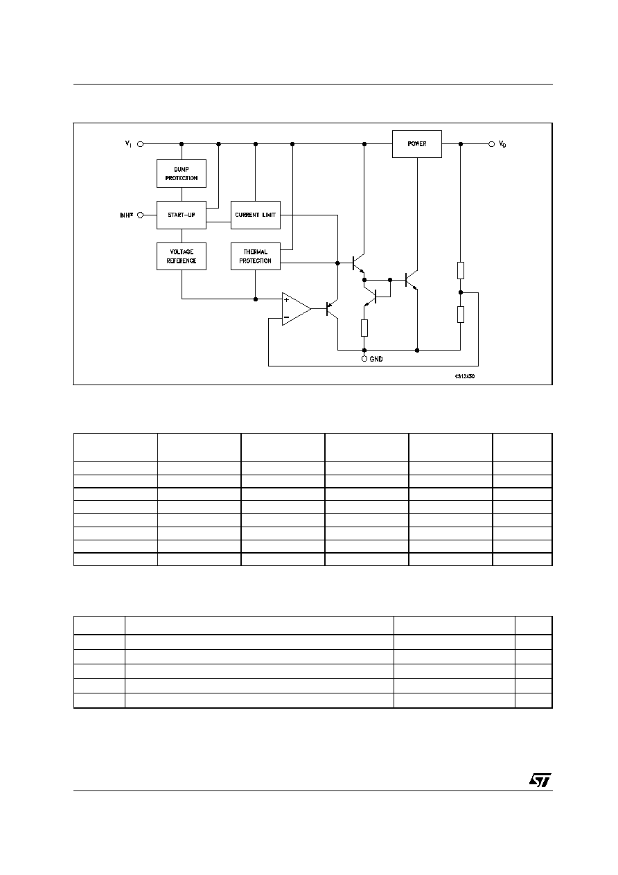
SCHEMATIC DIAGRAM FOR ADJUSTABLE VERSION
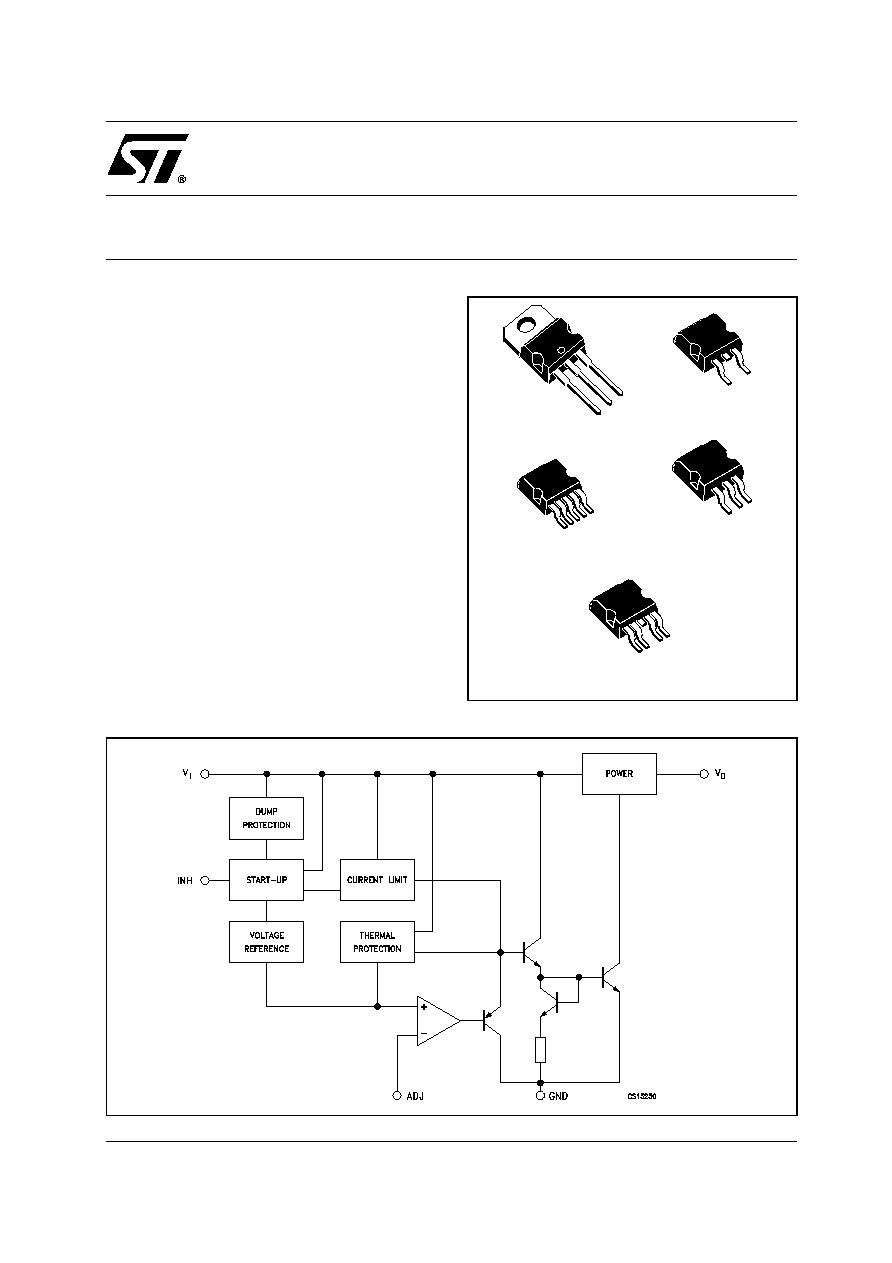
TO-220
D
2
PAK/A
D
2
PAK
P
2
PAK
P
2
PAK/A
LD29300 SERIES
2/17
SCHEMATIC DIAGRAM FOR FIXED VERSION
* Only for version with inhibit function.
ORDERING CODES
(*) Available in Tape & Reel with the suffix "R".
(#) Available on request.
ABSOLUTE MAXIMUM RATINGS
(*) Above 14V the device is automatically in shut-down.
Absolute Maximum Ratings are those beyond which damage to the device may occur. Functional operation under these condition is not im-
plied.
TO-220
D
2
PAK (*)
D
2
PAK/A (*)
P
2
PAK (*)(#)
P
2
PAK/A (*)
OUTPUT
VOLTAGE
LD29300V15
LD29300D2T15
LD29300D2M15
LD29300P2T15
LD29300P2M15
1.5 V
LD29300V18
LD29300D2T18
LD29300D2M18
LD29300P2T18
LD29300P2M18
1.8 V
LD29300V25
LD29300D2T25
LD29300D2M25
LD29300P2T25
LD29300P2M25
2.5 V
LD29300V33
LD29300D2T33
LD29300D2M33
LD29300P2T33
LD29300P2M33
3.3 V
LD29300V50
LD29300D2T50
LD29300D2M50
LD29300P2T50
LD29300P2M50
5.0 V
LD29300V80
LD29300D2T80
LD29300D2M80
LD29300P2T80
LD29300P2M80
8.0 V
LD29300V90
LD29300D2T90
LD29300D2M90
LD29300P2T90
LD29300P2M90
9.0 V
LD29300P2T
LD29300P2M
ADJ
Symbol
Parameter
Value
Unit
V
I
DC Input Voltage
30 (*)
V
I
O
Output Current
Internally Limited
mA
P
D
Power Dissipation
Internally Limited
mW
T
stg
Storage Temperature Range
-55 to 150
∞C
T
op
Operating Junction Temperature Range
-40 to 125
∞C
LD29300 SERIES
3/17
THERMAL DATA
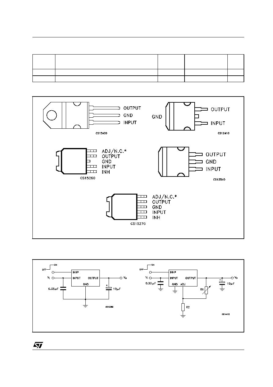
CONNECTION DIAGRAM (top view)
* Not connected for fixed version.
APPLICATION CIRCUIT
* Only for version with inhibit function.
Symbol
Parameter
TO-220
D
2
PAK-P
2
PAK
D
2
PAK/A-P
2
PAK/A
Unit
R
thj-case
Thermal Resistance Junction-case
3
3
∞C/W
R
thj-amb
Thermal Resistance Junction-ambient
50
60
∞C/W
TO-220
P
2
PAK/A
D
2
PAK
P
2
PAK
D
2
PAK/A
R
1
V
O
= V
REF
(1 +
)
R
2
LD29300 SERIES
4/17
ELECTRICAL CHARACTERISTICS OF LD29300#15
(I
O
= 10mA, T
J
= 25∞C, V
I
= 3.5V, V
INH
= 2V (Note 2), C
I
= 330nF, C
O
= 10
µ
F, unless otherwise specified)
NOTE 1: Guaranteed by design.
NOTE 2: Only for version with Inhibit function.
ELECTRICAL CHARACTERISTICS OF LD29300#18
(I
O
= 10mA, T
J
= 25∞C, V
I
= 3.8V, V
INH
= 2V (Note 3), C
I
= 330nF, C
O
= 10
µ
F, unless otherwise specified)
NOTE 1: Guaranteed by design.
NOTE 2: Dropout voltage is defined as the input-to-output differential when the output voltage drops to 99% of its nominal value with V
O
+1V
applied to V
I
.
NOTE 3: Only for version with Inhibit function.
Symbol
Parameter
Test Conditions
Min.
Typ.
Max.
Unit
V
I
Minimum Operating Input
Voltage
I
O
= 10mA to 3A
T
J
= -40 to 125∞C
2.5
V
V
O
Output Voltage
I
O
= 10mA to 3A, V
I
= 3 to 7V
T
J
= -40 to 125∞C
1.485
1.5
1.515
V
1.47
1.53
V
O
Load Regulation
I
O
= 10mA to 3A
0.2
1.0
%
V
O
Line Regulation
V
I
= 3 to 13V
0.06
0.5
%
SVR
Supply Voltage Rejection
f = 120 Hz, V
I
= 3.5
±
1V, I
O
= 1.5A
(Note 1)
65
75
dB
I
q
Quiescent Current
I
O
= 1.5A,
T
J
= -40 to 125∞C
20
50
mA
I
O
= 3A,
T
J
= -40 to 125∞C
45
100
V
I
= 13V, V
INH
= GND
T
J
= -40 to 125∞C
130
180
µA
I
sc
Short Circuit Current
V
I
- V
O
= 5.5V
4.5
A
V
IL
Control Input Logic Low
OFF MODE, (NOTE 2)
T
J
= -40 to 125∞C
0.8
V
V
IH
Control Input Logic High
ON MODE, (NOTE 2)
T
J
= -40 to 125∞C
2
V
I
INH
Control Input Current
T
J
= -40 to 125∞C
V
INH
= 13V
5
10
µA
eN
Output Noise Voltage
B
P
= 10Hz to 100KHz
I
O
= 100mA
60
µV
RMS
Symbol
Parameter
Test Conditions
Min.
Typ.
Max.
Unit
V
O
Output Voltage
I
O
= 10mA to 3A, V
I
= 3 to 7.3V
T
J
= -40 to 125∞C
1.782
1.8
1.818
V
1.764
1.836
V
O
Load Regulation
I
O
= 10mA to 3A
0.2
1.0
%
V
O
Line Regulation
V
I
= 3 to 13V
0.06
0.5
%
SVR
Supply Voltage Rejection
f = 120 Hz, V
I
= 3.8
±
1V, I
O
= 1.5A
(Note 1)
62
72
dB
V
DROP
Dropout Voltage
I
O
= 500mA, T
J
= -40 to 125∞C (Note 2)
0.1
V
I
O
= 1.5A,
T
J
= -40 to 125∞C (Note 2)
0.2
I
O
= 3A,
T
J
= -40 to 125∞C (Note 2)
0.4
0.7
I
q
Quiescent Current
I
O
= 1.5A,
T
J
= -40 to 125∞C
20
50
mA
I
O
= 3A,
T
J
= -40 to 125∞C
45
100
V
I
= 13V, V
INH
= GND
T
J
= -40 to 125∞C
130
180
µA
I
sc
Short Circuit Current
V
I
- V
O
= 5.5V
4.5
A
V
IL
Control Input Logic Low
OFF MODE, (NOTE 3)
T
J
= -40 to 125∞C
0.8
V
V
IH
Control Input Logic High
ON MODE, (NOTE 3)
T
J
= -40 to 125∞C
2
V
I
INH
Control Input Current
T
J
= -40 to 125∞C
V
INH
= 13V
5
10
µA
eN
Output Noise Voltage
B
P
= 10Hz to 100KHz
I
O
= 100mA
60
µV
RMS

LD29300 SERIES
5/17
ELECTRICAL CHARACTERISTICS OF LD29300#25
(I
O
= 10mA, T
J
= 25∞C, V
I
= 4.5V, V
INH
= 2V (Note 3), C
I
= 330nF, C
O
= 10
µ
F, unless otherwise specified)
NOTE 1: Guaranteed by design.
NOTE 2: Dropout voltage is defined as the input-to-output differential when the output voltage drops to 99% of its nominal value with V
O
+1V
applied to V
I
.
NOTE 3: Only for version with Inhibit function.
ELECTRICAL CHARACTERISTICS OF LD29300#33
(I
O
= 10mA, T
J
= 25∞C, V
I
= 5.3V, V
INH
= 2V (Note 3), C
I
= 330nF, C
O
= 10
µ
F, unless otherwise specified)
NOTE 1: Guaranteed by design.
NOTE 2: Dropout voltage is defined as the input-to-output differential when the output voltage drops to 99% of its nominal value with V
O
+1V
applied to V
I
.
NOTE 3: Only for version with Inhibit function.
Symbol
Parameter
Test Conditions
Min.
Typ.
Max.
Unit
V
O
Output Voltage
I
O
= 10mA to 3A, V
I
= 3.5 to 8V
T
J
= -40 to 125∞C
2.475
2.5
2.525
V
2.45
2.55
V
O
Load Regulation
I
O
= 10mA to 3A
0.2
1.0
%
V
O
Line Regulation
V
I
= 3.5 to 13V
0.06
0.5
%
SVR
Supply Voltage Rejection
f = 120 Hz, V
I
= 4.5
±
1V, I
O
= 1.5A
(Note 1)
55
70
dB
V
DROP
Dropout Voltage
I
O
= 500mA, T
J
= -40 to 125∞C (Note 2)
0.1
V
I
O
= 1.5A,
T
J
= -40 to 125∞C (Note 2)
0.2
I
O
= 3A,
T
J
= -40 to 125∞C (Note 2)
0.4
0.7
I
q
Quiescent Current
I
O
= 1.5A,
T
J
= -40 to 125∞C
20
50
mA
I
O
= 3A,
T
J
= -40 to 125∞C
45
100
V
I
= 13V, V
INH
= GND
T
J
= -40 to 125∞C
130
180
µA
I
sc
Short Circuit Current
V
I
- V
O
= 5.5V
4.5
A
V
IL
Control Input Logic Low
OFF MODE, (NOTE 3)
T
J
= -40 to 125∞C
0.8
V
V
IH
Control Input Logic High
ON MODE, (NOTE 3)
T
J
= -40 to 125∞C
2
V
I
INH
Control Input Current
T
J
= -40 to 125∞C
V
INH
= 13V
5
10
µA
eN
Output Noise Voltage
B
P
= 10Hz to 100KHz
I
O
= 100mA
100
µV
RMS
Symbol
Parameter
Test Conditions
Min.
Typ.
Max.
Unit
V
O
Output Voltage
I
O
= 10mA to 3A, V
I
= 4.3 to 8.8V
T
J
= -40 to 125∞C
3.267
3.3
3.333
V
3.234
3.366
V
O
Load Regulation
I
O
= 10mA to 3A
0.2
1.0
%
V
O
Line Regulation
V
I
= 4.3 to 13V
0.06
0.5
%
SVR
Supply Voltage Rejection
f = 120 Hz, V
I
= 5.3
±
1V, I
O
= 1.5A
(Note 1)
52
67
dB
V
DROP
Dropout Voltage
I
O
= 500mA, T
J
= -40 to 125∞C (Note 2)
0.1
V
I
O
= 1.5A,
T
J
= -40 to 125∞C (Note 2)
0.2
I
O
= 3A,
T
J
= -40 to 125∞C (Note 2)
0.4
0.7
I
q
Quiescent Current
I
O
= 1.5A,
T
J
= -40 to 125∞C
20
50
mA
I
O
= 3A,
T
J
= -40 to 125∞C
45
100
V
I
= 13V, V
INH
= GND
T
J
= -40 to 125∞C
130
180
µA
I
sc
Short Circuit Current
V
I
- V
O
= 5.5V
4.5
A
V
IL
Control Input Logic Low
OFF MODE, (NOTE 3)
T
J
= -40 to 125∞C
0.8
V
V
IH
Control Input Logic High
ON MODE, (NOTE 3)
T
J
= -40 to 125∞C
2
V
I
INH
Control Input Current
T
J
= -40 to 125∞C
V
INH
= 13V
5
10
µA
eN
Output Noise Voltage
B
P
= 10Hz to 100KHz
I
O
= 100mA
132
µV
RMS