1/10
February 2003
s
VERY LOW DROPOUT VOLTAGE
(0.2V TYP. AT 50mA LOAD)
s
VERY LOW QUIESCENT CURRENT
(TYP. 500µA AT 50mA LOAD)
s
OUTPUT CURRENT UP TO 50mA
s
LOGIC-CONTROLLED ELECTRONIC
SHUTDOWN
s
OUTPUT VOLTAGES OF 2.85; 3.0; 3.2; 3.3;
3.8; 5.0V
s
INTERNAL CURRENT AND THERMAL LIMIT
s
SUPPLY VOLTAGE REJECTION: 63dB (TYP)
s
ONLY 1µF FOR STABILITY
s
SELECTION AT 25∞C
s
TEMPERATURE RANGE: -25∞C TO 125∞C
s
PACKAGE AVAILABLE: SOT23-5L AND
TO-92
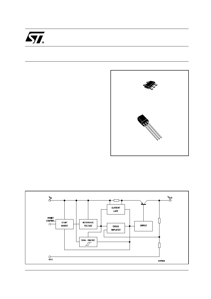
DESCRIPTION
The LD2979 series are very Low Drop regulators
available in SOT23-5L and TO-92.
The very low drop-voltage and the very low
quiescent current make them particularly suitable
for low noise, low power applications and in
battery powered systems.
Shutdown Logic Control function is available on
five pin version (TTL compatible). This means that
when the device is used as local regulator, it is
possible to put a part of the board in standby,
decreasing the total power consumption.
LD2979
SERIES
VERY LOW DROP
VOLTAGE REGULATORS WITH INHIBIT
SCHEMATIC DIAGRAM
SOT23-5L
TO-92
LD2979 SERIES
2/10
ABSOLUTE MAXIMUM RATINGS
Absolute Maximum Ratings are those values beyond which damage to the device may occur. Functional operation under these condition is
not implied.
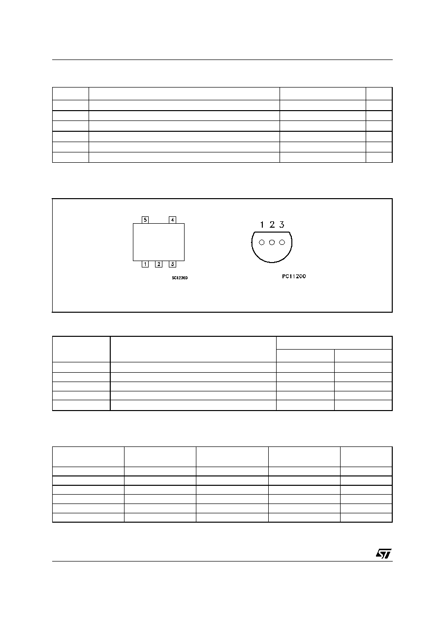
CONNECTION DIAGRAM (top view)
PIN DESCRIPTION
(*) Only for the version in SOT23-5L package: Inhibit pin is not internally pulled-up then it must not be left floating. Connect to a positive
voltage higher than 2V to able the device.
ORDERING CODES
Symbol
Parameter
Value
Unit
V
I
DC Input Voltage
16
V
V
INH
DC Inhibit Input Voltage
V
IN
V
I
O
Output Current
Internally limited
P
tot
Power Dissipation
Internally limited
T
stg
Storage Temperature Range
-40 to 150
∞C
T
op
Operating Junction Temperature Range
-25 to 125
∞C
SYMBOL
NAME AND FUNCTION
PIN NUMBER
SOT23-5L
TO-92
V
IN
Input Voltage
1
3
GND
Ground
2
2
INHIBIT
Control Switch ON/OFF (*)
3
NC
Not to be connected
4
V
OUT
Output Voltage
5
1
SOT23-5L (T&R)
TO-92
TO-92 (T&R)
TO-92 (Ammo Pack)
OUTPUT
VOLTAGES
LD2979M28TR
LD2979Z28
LD2979Z28TR
LD2979Z28AP
2.85 V
LD2979M30TR
LD2979Z30
LD2979Z30TR
LD2979Z30AP
3.0 V
LD2979M32TR
LD2979Z32
LD2979Z32TR
LD2979Z32AP
3.2 V
LD2979M33TR
LD2979Z33
LD2979Z33TR
LD2979Z33AP
3.3 V
LD2979M38TR
LD2979Z38
LD2979Z38TR
LD2979Z38AP
3.8 V
LD2979M50TR
LD2979Z50
LD2979Z50TR
LD2979Z50AP
5.0 V
SOT23-5L
TO-92

LD2979 SERIES
3/10
ELECTRICAL CHARACTERISTICS FOR LD2979 (refer to the test circuits, T
a
= 25∞C, V
IN
=V
O(NOM)
+1V,
I
O
=1mA, V
INH
=2V
(*)
, C
O
= 1
µ
F) (unless otherwise specified)
(*) Note: Only for types in SOT23-5L
Symbol
Parameter
Test Conditions
Min.
Typ.
Max.
Unit
V
O
Output Voltage
V
IN
= 3.85 V
2.793
2.85
2.907
V
I
O
= 1 to 50mA
T
a
= -25 to 125
∞C
2.736
2.964
V
O
Output Voltage
V
IN
= 4 V
2.940
3
3.060
V
I
O
= 1 to 50mA
T
a
= -25 to 125
∞C
2.880
3.120
V
O
Output Voltage
V
IN
= 4.2 V
3.136
3.2
3.264
V
I
O
= 1 to 50mA
T
a
= -25 to 125
∞C
3.072
3.328
V
O
Output Voltage
V
IN
= 4.3 V
3.234
3.3
3.366
V
I
O
= 1 to 50mA
T
a
= -25 to 125
∞C
3.168
3.432
V
O
Output Voltage
V
IN
= 4.8 V
3.724
3.8
3.876
V
I
O
= 1 to 50mA
T
a
= -25 to 125
∞C
3.648
3.952
V
O
Output Voltage
V
IN
= 6 V
4.9
5
5.1
V
I
O
= 1 to 50mA
T
a
= -25 to 125
∞C
4.8
5.2
I
out
Output Current Limit
100
mA
V
O
Line Regulation
V
IN
= V
O(NOM)
+1V to 16V, I
O
=
1mA
0.028
%/V
IN
T
a
= -25 to 125
∞C
0.064
I
d
Quiescent Current (On Mode) I
O
= 0
80
110
µ
A
I
O
= 0
T
a
= -25 to 125
∞C
170
I
O
= 50mA
500
700
I
O
= 50mA
T
a
= -25 to 125
∞C
1300
Quiescent Current (Off Mode)
(*)
V
INH
< 0.18 V
0
µ
A
V
INH
< 0.18 V
T
a
= -25 to 125
∞C
1
SVR
Supply Voltage Rejection
I
O
= 50mA
C
OUT
= 10
µ
F
f = 120Hz
63
dB
V
d
Dropout Voltage
I
O
= 0
6
12
mV
I
O
= 0
T
a
= -25 to 125
∞C
18
I
O
= 1mA
30
60
I
O
= 1mA
T
a
= -25 to 125
∞C
90
I
O
= 10mA
100
200
I
O
= 10mA
T
a
= -25 to 125
∞C
300
I
O
= 50mA
200
400
I
O
= 50mA
T
a
= -25 to 125
∞C
600
V
IL
Inhibit Input Logic Low
Device Off
T
a
= -25 to 125
∞C (*)
0.18
V
V
IH
Inhibit Input Logic High
Device On
T
a
= -25 to 125
∞C (*)
2
V
I
I
Inhibit Input Current
V
INH
= 0 V (*)
0
-1
µ
A
V
INH
= 5V
T
a
= -25 to 125
∞C
5
15
eN
Output Noise Voltage (RMS)
BW= 300Hz to 50KHz
C
O
= 10
µ
F
160
µ
V
LD2979 SERIES
4/10
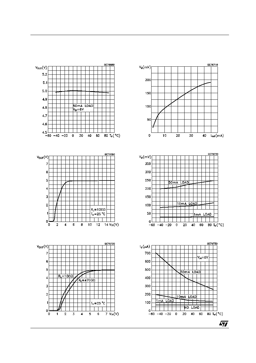
TYPICAL CHARACTERISTICS (unless otherwise specified T
a
= 25∞C)
Figure 1 : Output Voltage vs Temperature
Figure 2 : Output Voltage vs Input Voltage
Figure 3 : Output Voltage vs Input Voltage
Figure 4 : Dropout Voltage vs Output Current
Figure 5 : Dropout Voltage vs Temperature
Figure 6 : Quiescent Current vs Temperature

LD2979 SERIES
5/10
Figure 7 : Short Circuit Current vs Dropout
Voltage
Figure 8 : Supply Voltage Rejection vs
Frequency
Figure 9 : Inhibit Current vs Temperature
Figure 10 : Inhibit Voltage vs Temperature
Figure 11 : Load Transient Response
Figure 12 : Load Transient Response
C
O
= 10
µ
F (ESR = 1 at 1KHz)
C
O
= 10
µ
F (ESR = 1 at 1KHz)