 | –≠–ª–µ–∫—Ç—Ä–æ–Ω–Ω—ã–π –∫–æ–º–ø–æ–Ω–µ–Ω—Ç: LD2979Z30 | –°–∫–∞—á–∞—Ç—å:  PDF PDF  ZIP ZIP |
LD2979
SERIES
VERY LOW DROP
VOLTAGE REGULATORS WITH INHIBIT
April 2000
s
VERY LOW DROPOUT VOLTAGE
(0.2V TYP. AT 50mA LOAD)
s
VERY LOW QUIESCENT CURRENT
(TYP. 500
µ
A AT50mA LOAD)
s
OUTPUT CURRENT UP TO 50 mA
s
LOGIC-CONTROLLED ELECTRONIC
SHUTDOWN
s
OUTPUT VOLTAGES OF 2.85; 3.0; 3.2; 3.3;
3.8; 5.0V
s
INTERNAL CURRENT AND THERMAL LIMIT
s
SUPPLY VOLTAGE REJECTION: 63dB (TYP)
s
ONLY 1
µ
F FOR STABILITY
s
SELECTION AT 25
o
C
s
TEMPERATURE RANGE: -25 TO 125
o
C
s
PACKAGE AVAILABLE:SOT23-5L AND TO-92
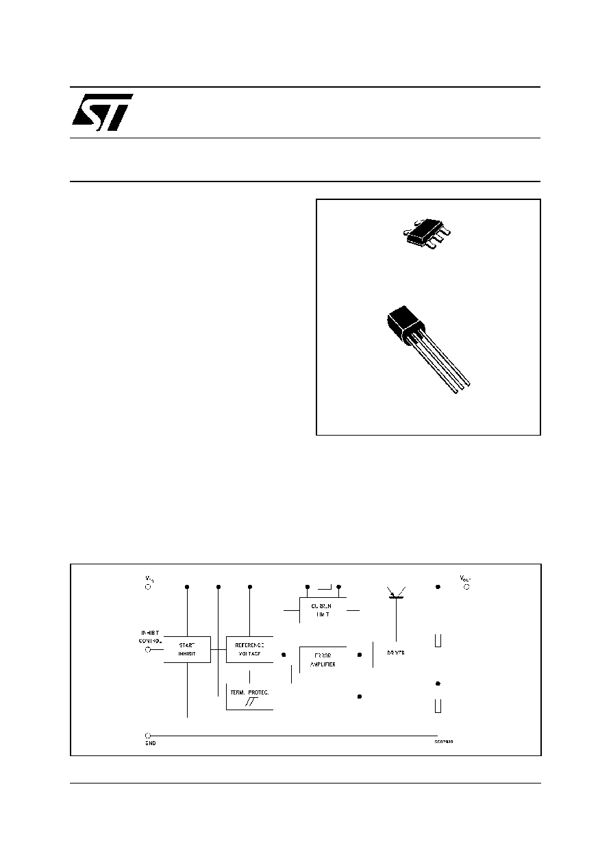
DESCRIPTION
The LD2979 series are very Low Drop regulators
available in SOT23-5L and TO-92.
The very low drop-voltage and the very low
quiescent current make them particularly suitable
for low noise, low power applications and in
battery powered systems.
Shutdown Logic Control function is available on
five pin version (TTL compatible). This means
that when the device is used as local regulator, it
is possible to put a part of the board in standby,
decreasing the total power consumption.
SCHEMATIC DIAGRAM
SOT23-5L
TO-92
Æ
1/9
ABSOLUTE MAXIMUM RATING
Symbol
Parameter
Value
Unit
V
IN
DC Input Voltage
16
V
V
I NH
DC Inhibit Input Voltage
V
I N
V
I
o
Output Current
I nternally limited
mA
P
tot
Power Dissipation
I nternally limited
mW
T
st g
Storage Temperature Range
- 40 to 150
o
C
T
op
Operating Junction Temperature Range
- 25 to 125
o
C
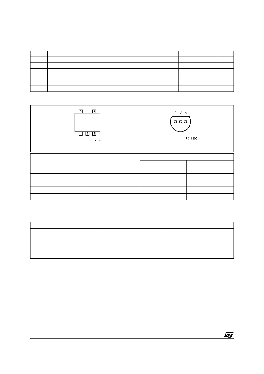
CONNECTION DIAGRAM (top view)
ORDERING NUMBERS
SOT23-5L
TO-92
Output Voltage
LD2979M28
LD2979M30
LD2979M32
LD2979M33
LD2979M38
LD2979M50
LD2979Z28
LD2979Z30
LD2979Z32
LD2979Z33
LD2979Z38
LD2979Z50
2.85 V
3. 0 V
3. 2 V
3. 3 V
3. 8 V
5. 0 V
SOT23-5L
TO-92
BOTTOM
VIEW
SYMBOL
NAME AND FUNCTION
PIN NUMBER
SO T23-5L
T O-92
V
I N
Input Voltage
1
3
GND
Ground
2
2
I NHIBIT
Control Switch ON/OF F (*)
3
-
NC
Not to be connected
4
-
V
OUT
Output Voltage
5
1
(*) Only for the version in SOT23-5L package: Inhibit pin is not internally pulled-up then it must not be left floating. Connect to a positive
voltage higher than 2V to able the device.
LD2979
2/9

ELECTRICAL CHARACTERISTICS FOR LD2979 (refer to the test circuits, T
a
= 25
o
C,
V
IN
= V
O(NOM)
+1, C
O
= 1
µ
F, I
O
= 1mA, V
inh
= 2V
(*)
) (unless otherwise specified)
Symbol
Parameter
Test Conditions
Min.
Typ.
Max.
Unit
V
o
Output Voltage
V
IN
= 3.85 V
1 < I
o
< 50 mA,
-25 < T
a
< 125
o
C
2.793
2.736
2.85
2. 907
2. 964
V
V
V
o
Output Voltage
V
IN
= 4 V
1 < I
o
< 50 mA,
-25 < T
a
< 125
o
C
2.940
2.880
3
3. 060
3. 120
V
V
V
o
Output Voltage
V
IN
= 4.2 V
1 < I
o
< 50 mA,
-25 < T
a
< 125
o
C
3.136
3.072
3.2
3. 264
3. 328
V
V
V
o
Output Voltage
V
IN
= 4.3 V
1 < I
o
< 50 mA,
-25 < T
a
< 125
o
C
3.234
3.168
3.3
3. 366
3. 432
V
V
V
o
Output Voltage
V
IN
= 4.8 V
1 < I
o
< 50 mA,
-25 < T
a
< 125
o
C
3.724
3.648
3.8
3. 876
3. 952
V
V
V
o
Output Voltage
V
IN
= 6 V
1 < I
o
< 50 mA,
-25 < T
a
< 125
o
C
4.9
4.8
5
5.1
5.2
V
V
I
o ut
Output Current Limit
100
mA
V
o
Line Regulation
V
O(NOM)
+1 < V
IN
< 16V,
I
o
= 1 mA
-25 < T
a
< 125
o
C
0. 028
0. 064
%/ V
in
I
d
Quiescent Current
ON MODE
I
o
= 0 mA
I
o
= 0 mA
-25 < T
a
< 125
o
C
I
o
= 50 mA
I
o
= 50 mA
-25 < T
a
< 125
o
C
80
500
110
170
700
1300
µ
A
µ
A
µ
A
µ
A
OFF MODE (*)
V
ihn
< 0.18 V
V
ihn
< 0.18 V -25 < T
a
< 125
o
C
0
1
µ
A
µ
A
SVR
Supply Voltage Rejection
I
o
= 50 mA, f = 120 Hz, C
out
= 10
µ
F
63
dB
V
d
Dropout Voltage
I
o
= 0 mA
I
o
= 0 mA
-25 < T
a
< 125
o
C
I
o
= 1 mA
I
o
= 1 mA
-25 < T
a
< 125
o
C
I
o
= 10 mA
I
o
= 10 mA
-25 < T
a
< 125
o
C
I
o
= 50 mA
I
o
= 50 mA
-25 < T
a
< 125
o
C
6
30
100
200
12
18
60
90
200
300
400
600
mV
mV
mV
mV
mV
mV
mV
mV
V
il
Control Input Logic Low
-25 < T
a
< 125
o
C (*)
Device Off
0.18
V
V
ih
Control Input Logic High
-25 < T
a
< 125
o
C (*)
Device On
2
V
I
i
Control Input Current
V
inhibit
= 0 V (*)
V
inhibit
= 5 V,
-25 < T
a
< 125
o
C (*)
0
5
-1
15
µ
A
µ
A
eN
Output Noise Voltage (RMS)
BW = 300 Hz to 50 KHz, C
out
= 10
µ
F
160
µ
V
(*) Note: Only for types in SOT23-5L
LD2979
3/9
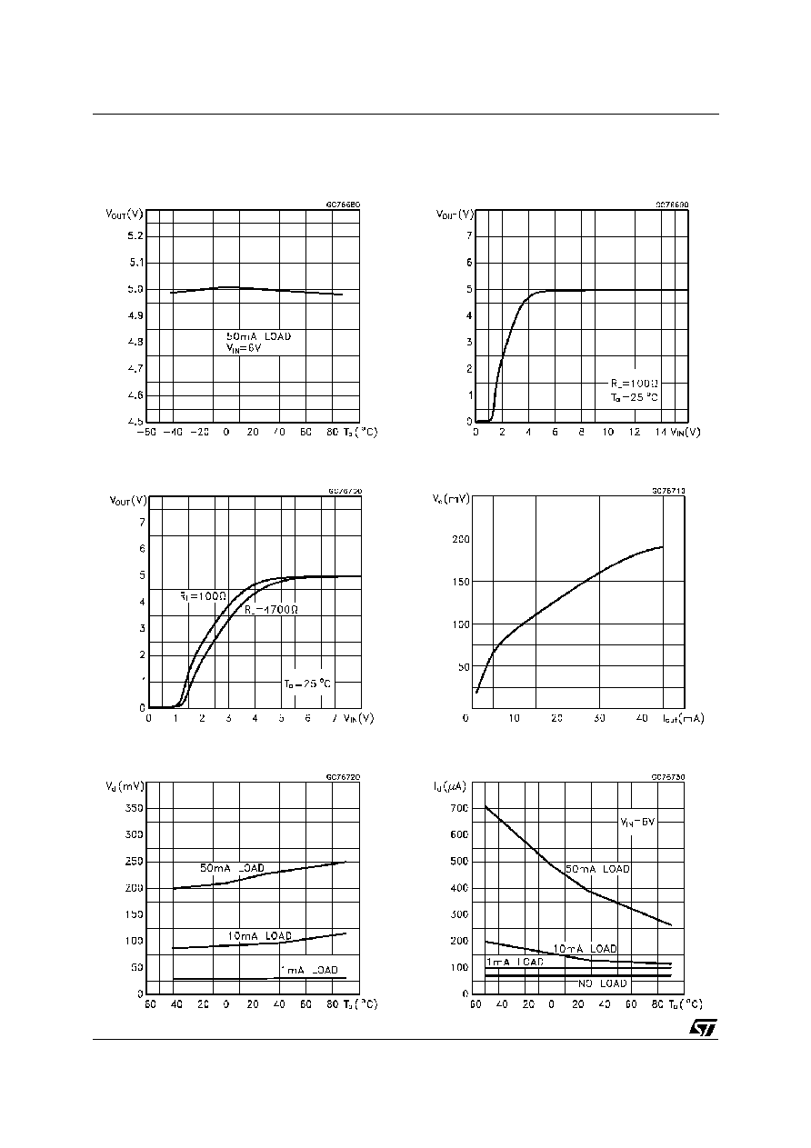
Output Voltage vs Temperature
Output Voltage vs Input Voltage
Dropout Voltage vs Temperature
Dropout Voltage vs Output Current
Quiescent Current vs Temperature
TYPICAL PERFORMANCE CHARACTERISTICS (unless otherwise specified T
a
=25
o
C)
Output Voltage vs Input Voltage
LD2979
4/9

Short Circuit Current vs Dropout Voltgae
Inhibit Current vs Temperature
Vout
Iout
Vin: 5V, Iout: 1mA to 50mA, Time : 10us/DIV
Vout
20mV/ DIV
Iout
20mA/ DIV
Inhibit Voltage vs Temperature
Vout
Iout
Vin: 5V, Iout: 50mA to 1mA, Time : 10us/DIV
Vout
20mV/ DIV
Iout
20mA/ DIV
Load Transient Response
TYPICAL PERFORMANCE CHARACTERISTICS (continued)
S.V.R. vs Frequency
Load Transient Response
C
O
= 10
µ
F (ESR=1
at 1KHz)
C
O
= 10
µ
F (ESR=1
at 1KHz)
LD2979
5/9