ChipFind - документация

Электронный компонент: LD2981CXX25

Скачать:  PDF   ZIP
1/17
September 2003
s
STABLE WITH LOW ESR CERAMIC
CAPACITORS
s
ULTRA LOW DROPOUT VOLTAGE (0.17V
TYP. AT 100mA LOAD, 7mV TYP. AT 1mA
LOAD)
s
VERY LOW QUIESCENT CURRENT (80A
TYP. AT NO LOAD IN ON MODE; MAX 1A
IN OFF MODE)
s
GUARANTEED OUTPUT CURRENT UP TO
100mA
s
LOGIC-CONTROLLED ELECTRONIC
SHUTDOWN
s
OUTPUT VOLTAGE OF 1.5; 1.8; 2.5; 2.85;
3.0; 3.2; 3.3; 3.6; 3.8; 4.0; 4.7; 4.85; 5.0V
s
INTERNAL CURRENT AND THERMAL LIMIT
s
0.75% TOLERANCE OUTPUT VOLTAGE
AVAILABLE (A VERSION)
s
OUTPUT LOW NOISE VOLTAGE 160VRMS
s
TEMPERATURE RANGE: -40 TO 125C
s
SMALLEST PACKAGE SOT23-5L AND
SOT-89
s
FAST DYNAMIC RESPONSE TO LINE AND
LOAD CHANGES
DESCRIPTION
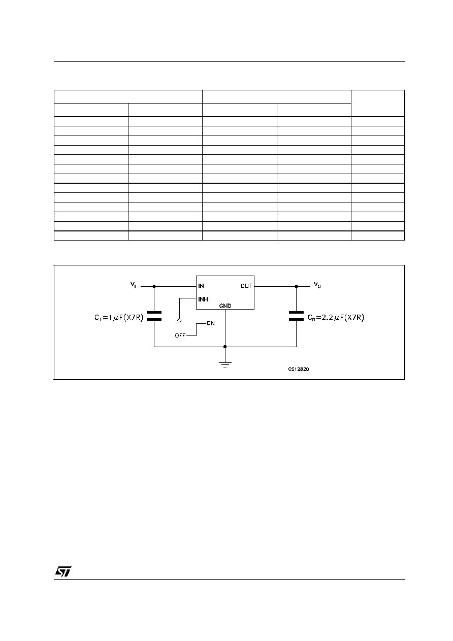
The LD2981 series are 100mA fixed-output
voltage regulator. The low drop-voltage and the
ultra low quiescent current make them suitable for
low noise, low power applications and in battery
powered systems.
The quiescent current in sleep mode is less than
1A when INHIBIT pin is pulled low. Shutdown
Logic Control function is available on pin n.3 (TTL
compatible). This means that when the device is
used as local regulator, it is possible to put a part
of the board in standby, decreasing the total
power consumption. The LD2981 is designed to
work with low ESR ceramic capacitor. Typical
applications are in cellular phone, palmtop/laptop
computer,
personal
digital
assistant
(PDA),
personal stereo, camcorder and camera.
LD2981
SERIES
ULTRA LOW DROP VOLTAGE REGULATORS WITH INHIBIT
LOW ESR OUTPUT CAPACITORS COMPATIBLE
SCHEMATIC DIAGRAM
SOT23-5L
SOT-89
LD2981 SERIES
2/17
ABSOLUTE MAXIMUM RATINGS
Absolute Maximum Ratings are those values beyond which damage to the device may occur. Functional operation under these condition is
not implied.
THERMAL DATA
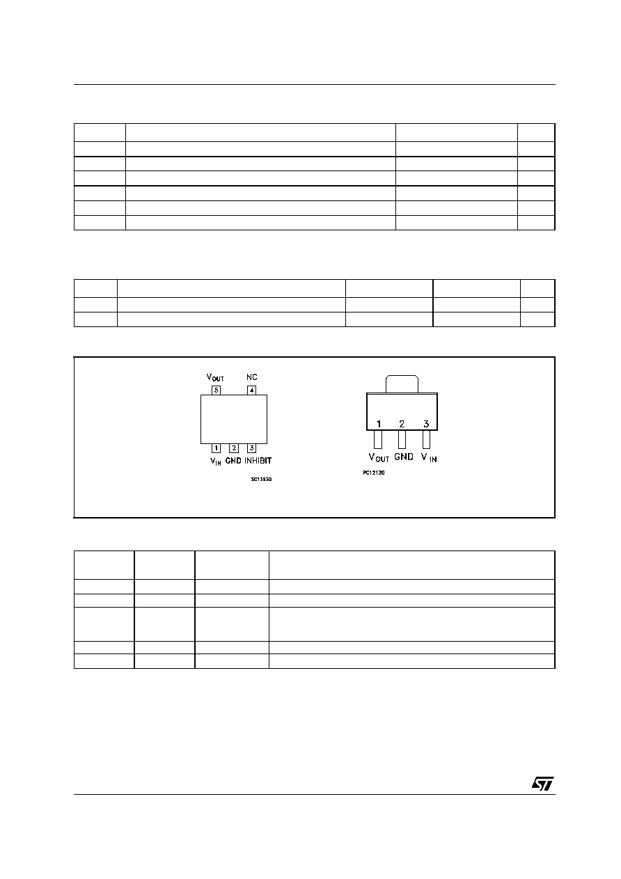
CONNECTION DIAGRAM (top view)
PIN DESCRIPTION
Symbol
Parameter
Value
Unit
V
I
DC Input Voltage
-0.3 to 16
V
V
INH
INHIBIT Input Voltage
-0.3 to 16
V
I
O
Output Current
Internally limited
P
D
Power Dissipation
Internally limited
T
STG
Storage Temperature Range
-55 to 150
C
T
OP
Operating Junction Temperature Range
-40 to 125
C
Symbol
Parameter
SOT23-5L
SOT-89
Unit
R
thj-case
Thermal Resistance Junction-case
81
15
C/W
R
thj-amb
Thermal Resistance Junction-ambient
255
110
C/W
Pin N
SOT23-5L
Pin N
SOT-89
Symbol
Name and Function
1
3
V
IN
Input Port
2
2
GND
Ground Pin
3
INHIBIT
Control switch ON/OFF. Inhibit is not internally pulled-up; it cannot be
left floating. Disable the device when connected to GND or to a
positive voltage less than 0.18V
4
NC
Not Connected
5
1
V
OUT
Output Port
SOT23-5L
SOT-89
LD2981 SERIES
3/17
ORDERING CODES
TYPICAL APPLICATION CIRCUIT
(*) Inhibit Pin is not internally pulled-up then it must not be left floating. Disable the device when connected to GND or to a positive voltage
less than 0.18V.
AB VERSION
C VERSION
OUTPUT
VOLTAGES
SOT23-5L
SOT-89
SOT23-5L
SOT-89
LD2981CM15TR
LD2981CU15TR
1.5 V
LD2981CM18TR
LD2981CU18TR
1.8 V
LD2981ABM25TR
LD2981ABU25TR
LD2981CM25TR
LD2981CU25TR
2.5 V
LD2981ABM28TR
LD2981ABU28TR
LD2981CM28TR
LD2981CU28TR
2.85 V
LD2981ABM30TR
LD2981ABU30TR
LD2981CM30TR
LD2981CU30TR
3.0 V
LD2981ABM32TR
LD2981ABU32TR
LD2981CM32TR
LD2981CU32TR
3.2 V
LD2981ABM33TR
LD2981ABU33TR
LD2981CM33TR
LD2981CU33TR
3.3 V
LD2981ABM36TR
LD2981ABU36TR
LD2981CM36TR
LD2981CU36TR
3.6 V
LD2981ABM38TR
LD2981ABU38TR
LD2981CM38TR
LD2981CU38TR
3.8 V
LD2981ABM40TR
LD2981ABU40TR
LD2981CM40TR
LD2981CU40TR
4.0 V
LD2981ABM47TR
LD2981ABU47TR
LD2981CM47TR
LD2981CU47TR
4.7 V
LD2981ABM48TR
LD2981ABU48TR
LD2981CM48TR
LD2981CU48TR
4.85 V
LD2981ABM50TR
LD2981ABU50TR
LD2981CM50TR
LD2981CU50TR
5.0 V
LD2981 SERIES
4/17
ELECTRICAL CHARACTERISTICS FOR LD2981AB (T
j
= 25C, V
I
= V
O(NOM)
+1V, C
I
= 1
F(X7R),
C
O
= 2.2
F(X7R), I
O
= 1mA, V
INH
= 2V, unless otherwise specified)
Symbol
Parameter
Test Conditions
Min.
Typ.
Max.
Unit
V
OP
Operating Input Voltage
2.5
16
V
V
O
Output Voltage
I
O
= 1 mA
2.481
2.5
2.518
V
I
O
= 1 to 100 mA
2.475
2.525
I
O
= 1 to 100 mA
T
J
= -40 to 125
C
2.437
2.562
V
O
Output Voltage
I
O
= 1 mA
2.828
2.85
2.872
V
I
O
= 1 to 100 mA
2.822
2.878
I
O
= 1 to 100 mA
T
J
= -40 to 125
C
2.779
2.921
V
O
Output Voltage
I
O
= 1 mA
2.977
3
3.023
V
I
O
= 1 to 100 mA
2.970
3.030
I
O
= 1 to 100 mA
T
J
= -40 to 125
C
2.925
3.075
V
O
Output Voltage
I
O
= 1 mA
3.176
3.2
3.224
V
I
O
= 1 to 100 mA
3.168
3.232
I
O
= 1 to 100 mA
T
J
= -40 to 125
C
3.12
3.28
V
O
Output Voltage
I
O
= 1 mA
3.275
3.3
3.325
V
I
O
= 1 to 100 mA
3.267
3.333
I
O
= 1 to 100 mA
T
J
= -40 to 125
C
3.217
3.383
V
O
Output Voltage
I
O
= 1 mA
3.573
3.6
3.627
V
I
O
= 1 to 100 mA
3.564
3.636
I
O
= 1 to 100 mA
T
J
= -40 to 125
C
3.510
3.690
V
O
Output Voltage
I
O
= 1 mA
3.771
3.8
3.829
V
I
O
= 1 to 100 mA
3.762
3.838
I
O
= 1 to 100 mA
T
J
= -40 to 125
C
3.705
3.895
V
O
Output Voltage
I
O
= 1 mA
3.97
4
4.03
V
I
O
= 1 to 100 mA
3.96
4.04
I
O
= 1 to 100 mA
T
J
= -40 to 125
C
3.9
4.1
V
O
Output Voltage
I
O
= 1 mA
4.664
4.7
4.735
V
I
O
= 1 to 100 mA
4.653
4.747
I
O
= 1 to 100 mA
T
J
= -40 to 125
C
4.582
4.817
V
O
Output Voltage
I
O
= 1 mA
4.813
4.85
4.887
V
I
O
= 1 to 100 mA
4.801
4.899
I
O
= 1 to 100 mA
T
J
= -40 to 125
C
4.729
4.971
V
O
Output Voltage
I
O
= 1 mA
4.962
5
5.038
V
I
O
= 1 to 100 mA
4.950
5.050
I
O
= 1 to 100 mA
T
J
= -40 to 125
C
4.875
5.125
V
O
Line Regulation
V
O(NOM)
+ 1 < V
IN
< 16 V
I
O
= 1 mA
0.003
0.014
%/V
T
J
= -40 to 125
C
0.032
LD2981 SERIES
5/17
(NOTE 1): For Vo < 2.5V dropout voltage can be calculated according to the minimum input voltage in full temperature range.
I
Q
Quiescent Current
ON MODE
I
O
= 0
80
100
A
I
O
= 0
T
J
= -40 to 125
C
150
I
O
= 1 mA
100
150
I
O
= 1 mA
T
J
= -40 to 125
C
200
I
O
= 25 mA
250
400
I
O
= 25 mA
T
J
= -40 to 125
C
800
I
O
= 100 mA
1000
1300
I
O
= 100 mA
T
J
= -40 to 125
C
2600
OFF MODE
V
INH
< 0.3 V
0.8
V
INH
< 0.15 V
T
J
= -40 to 125
C
2
V
DROP
Dropout Voltage (NOTE 1)
I
O
= 0
1
3
mV
I
O
= 0
T
J
= -40 to 125
C
5
I
O
= 1mA
7
10
I
O
= 1mA
T
J
= -40 to 125
C
15
I
O
= 25mA
70
100
I
O
= 25mA
T
J
= -40 to 125
C
150
I
O
= 100mA
180
250
I
O
= 100mA
T
J
= -40 to 125
C
375
I
SC
Short Circuit Current
R
L
= 0
150
mA
SVR
Supply Voltage Rejection
C
O
= 10
F
f = 1KHz
63
dB
V
INH
Inhibit Input Logic Low
LOW = Output OFF
T
J
= -40 to 125
C
0.18
V
V
INL
Inhibit Input Logic High
HIGH = Output ON
T
J
= -40 to 125
C
1.6
V
I
INH
Inhibit Input Current
V
INH
= 0V
T
J
= -40 to 125
C
0
-1
A
V
INH
= 5V
T
J
= -40 to 125
C
5
15
e
N
Output Noise Voltage
B
W
= 300 Hz to 50 KHz
C
O
= 10
F
160
V
RMS
T
SHDN
Thermal Shutdown
170
C
Symbol
Parameter
Test Conditions
Min.
Typ.
Max.
Unit