1/13
July 2003
s
VERY LOW DROPOUT VOLTAGE (120mV
AT 50mA AND 7mV AT 1mA LOAD)
s
VERY LOW QUIESCENT CURRENT (375
µ
A
TYP. AT 50mA LOAD AND 75
µ
A AT 1mA)
s
OUTPUT CURRENT UP TO 50mA
s
LOGIC CONTROLLED ELECTRONIC
SHUTDOWN
s
OUTPUT VOLTAGE OF 1.5,1.8, 2.5, 2.8, 2.85,
3, 3.1, 3.2, 3.3, 3.5, 3.6, 3.8, 4, 4.7, 5V
s
INTERNAL CURRENT AND THERMAL LIMIT
s
AVAILABLE IN
±
1% TOLLERANCE (AT 25∞C,
A VERSION)
s
SUPPLY VOLTAGE REJECTION: 45dB (TYP)
s
ONLY 1µF FOR STABILITY
s
LOW OUTPUT NOISE VOLTAGE 30µVrms
s
SMALLEST PACKAGE SOT23-5L
s
TEMPERATURE RANGE: -40∞C TO 125∞C
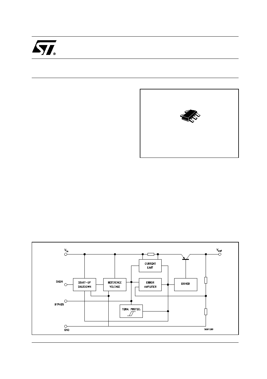
DESCRIPTION
The LD2982 is a 50mA fixed output voltage
regulator. The ultra low drop voltage and the low
quiescent current make them particularly suitable
for low noise, low power applications, and in
battery
powered
systems.
In
sleep
mode
quiescent current is less than 1µA when INHIBIT
pin is pulled low. Shutdown Logic Control Function
is available on pin 3 (TTL compatible). This means
that when the device is used as local regulator, it
is possible to put a part of the board in standby,
decreasing the total power consumption.
An external capacitor C
BYP
=10nF connected
between bypass pin and GND
reduce the noise
to 30µVrms.
Typical application are in cellular phone, palmtop/
laptop computer, personal digital assistant (PDA),
personal stereo, camcorder and camera.
LD2982
SERIES
VERY LOW DROP AND LOW NOISE VOLTAGE REGULATOR
WITH INHIBIT FUNCTION, LOW ESR CAP. COMPATIBLE
SCHEMATIC DIAGRAM
SOT23-5L
LD2982 SERIES
2/13
ABSOLUTE MAXIMUM RATINGS
Absolute Maximum Ratings are those values beyond which damage to the device may occur. Functional operation under these condition is
not implied.
THERMAL DATA
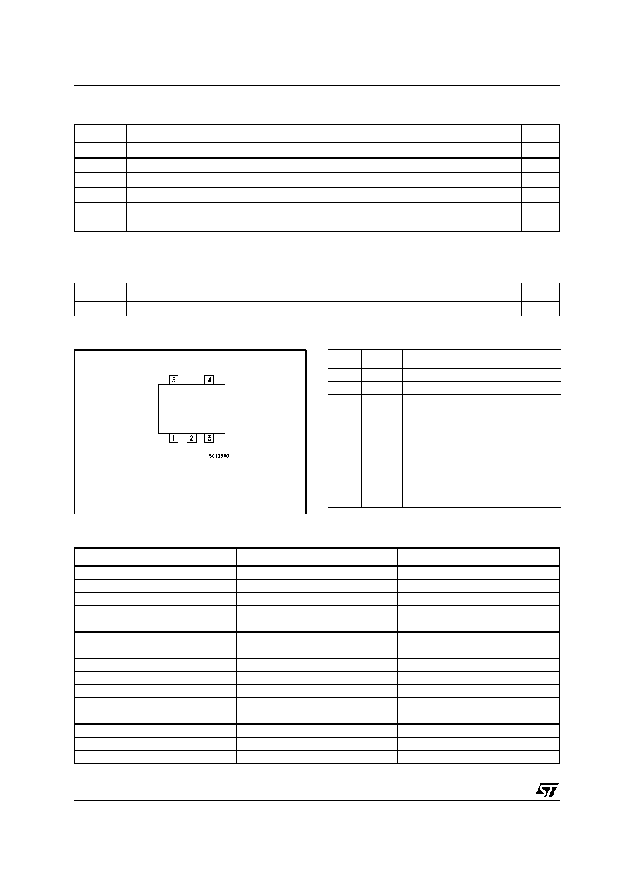
CONNECTION DIAGRAM (top view)
PIN DESCRIPTION
ORDERING CODES
Symbol
Parameter
Value
Unit
V
I
DC Input Voltage
16
V
V
INH
INHIBIT Input Voltage
16
V
I
O
Output Current
Internally limited
P
tot
Power Dissipation
Internally limited
T
stg
Storage Temperature Range
-65 to +150
∞C
T
op
Operating Junction Temperature Range
-40 to +125
∞C
Symbol
Parameter
SOT23-5L
Unit
R
thj-case
Thermal Resistance Junction-case
81
∞C/W
SOT23-5L
Pin N∞ Symbol
Name and Function
1
IN
Input Port
2
GND
Ground Pin
3
INHIBIT Control switch ON/OFF. Inhibit is not
internally pulled-up; it cannot be left
floating. Disable the device when
connected to GND or to a positive
voltage less than 0.18V
4
Bypass Bypass Pin: Capacitor to be
connected to GND in order to
improve the thermal noise
performances.
5
OUT
Output Port
A VERSION
B VERSION
OUTPUT VOLTAGES
LD2982AM15R
LD2982BM15R
1.5V
LD2982AM18R
LD2982BM18R
1.8V
LD2982AM25R
LD2982BM25R
2.5V
LD2982AM28R
LD2982BM28R
2.8V
LD2982AM285R
LD2982BM285R
2.85V
LD2982AM30R
LD2982BM30R
3.0V
LD2982AM31R
LD2982BM31R
3.1V
LD2982AM32R
LD2982BM32R
3.2V
LD2982AM33R
LD2982BM33R
3.3V
LD2982AM35R
LD2982BM35R
3.5V
LD2982AM36R
LD2982BM36R
3.6V
LD2982AM38R
LD2982BM38R
3.8V
LD2982AM40R
LD2982BM40R
4.0V
LD2982AM47R
LD2982BM47R
4.7V
LD2982AM50R
LD2982BM50R
5.0V