1/13
July 2003
s
VERY LOW DROPOUT VOLTAGE (280mV
AT 150mA AND 7mV AT 1mA LOAD)
s
VERY LOW QUIESCENT CURRENT (2mA
TYP. AT 150mA LOAD AND 80
µ
A AT NO
LOAD)
s
OUTPUT CURRENT UP TO 150mA
s
LOGIC CONTROLLED ELECTRONIC
SHUTDOWN
s
OUTPUT VOLTAGE OF 1.5, 1.8, 2.5, 2.8,
2.85, 3, 3.1, 3.2, 3.3, 3.5, 3.6, 3.8, 4, 4.7, 5V
s
INTERNAL CURRENT AND THERMAL LIMIT
s
AVAILABLE IN
±
1% TOLLERANCE (AT 25∞C,
A VERSION)
s
LOW OUTPUT NOISE VOLTAGE 30
µ
Vrms
s
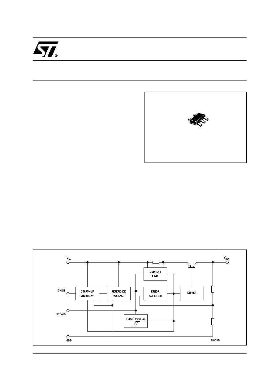
SMALLEST PACKAGE SOT23-5L
s
TEMPERATURE RANGE: -40∞C TO 125∞C
DESCRIPTION
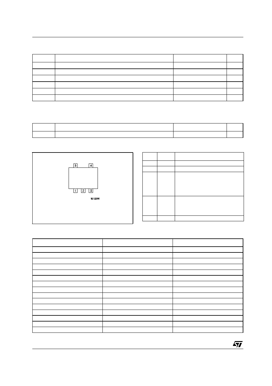
The LD2985 is a 150mA fixed output voltage
regulator. The ultra low drop voltage and the low
quiescent current make them particularly suitable
for low noise, low power applications, and in
battery
powered
systems.
In
sleep
mode
quiescent current is less than 1µA when INHIBIT
pin is pulled low. Shutdown Logic Control Function
is available on pin 3 (TTL compatible). This means
that when the device is used as local regulator, it
is possible to put a part of the board in standby,
decreasing the total power consumption.
An external capacitor, C
BYP
=10nF, connected
between bypass pin and GND
reduce the noise
to 30µVrms.
Typical application are in cellular phone, palmtop
laptop computer, personal digital assistant (PDA),
personal stereo, camcorder and camera.
LD2985
SERIES
VERY LOW DROP AND LOW NOISE VOLTAGE REGULATOR
LOW ESR CAP. COMPATIBLE, WITH INHIBIT FUNCTION
SCHEMATIC DIAGRAM
SOT23-5L
LD2985 SERIES
2/13
ABSOLUTE MAXIMUM RATINGS
Absolute Maximum Ratings are those values beyond which damage to the device may occur. Functional operation under these condition is
not implied.
THERMAL DATA
CONNECTION DIAGRAM (top view)
PIN DESCRIPTION
ORDERING CODES
Symbol
Parameter
Value
Unit
V
I
DC Input Voltage
16
V
V
INH
INHIBIT Input Voltage
16
V
I
O
Output Current
Internally limited
P
tot
Power Dissipation
Internally limited
T
stg
Storage Temperature Range
-65 to +150
∞C
T
op
Operating Junction Temperature Range
-40 to +125
∞C
Symbol
Parameter
SOT23-5L
Unit
R
thj-case
Thermal Resistance Junction-case
81
∞C/W
SOT23-5L
Pin N∞ Symbol
Name and Function
1
IN
Input Port
2
GND
Ground Pin
3
INHIBIT Control switch ON/OFF. Inhibit is not
internally pulled-up; it cannot be left
floating. Disable the device when
connected to GND or to a positive
voltage less than 0.18V
4
Bypass Bypass Pin: Capacitor to be
connected to GND in order to
improve the thermal noise
performances.
5
OUT
Output Port
A VERSION
B VERSION
OUTPUT VOLTAGES
LD2985AM15R
LD2985BM15R
1.5V
LD2985AM18R
LD2985BM18R
1.8V
LD2985AM25R
LD2985BM25R
2.5V
LD2985AM28R
LD2985BM28R
2.8V
LD2985AM285R
LD2985BM285R
2.85V
LD2985AM30R
LD2985BM30R
3.0V
LD2985AM31R
LD2985BM31R
3.1V
LD2985AM32R
LD2985BM32R
3.2V
LD2985AM33R
LD2985BM33R
3.3V
LD2985AM35R
LD2985BM35R
3.5V
LD2985AM36R
LD2985BM36R
3.6V
LD2985AM38R
LD2985BM38R
3.8V
LD2985AM40R
LD2985BM40R
4.0V
LD2985AM47R
LD2985BM47R
4.7V
LD2985AM50R
LD2985BM50R
5.0V

LD2985 SERIES
3/13
ELECTRICAL CHARACTERISTICS FOR LD2985A (T
J
= 25∞C, V
I
=V
O
+1V, I
O
=1mA, V
SHDN
=2V,
C
I
= 1
µ
F, C
O
= 1
µ
F, unless otherwise specified)
Symbol
Parameter
Test Conditions
Min.
Typ.
Max.
Unit
V
Op
Operating Input Voltage
2.5
16
V
V
O
Output Voltage
V
I
= 2.5V
1.485
1.5
1.515
V
I
O
= 1 to 50mA
1.462
1.538
V
I
O
= 1 to 50mA
T
J
= -40 to 125
∞C
1.447
1.553
V
V
O
Output Voltage
V
I
= 2.8V
1.782
1.8
1.818
V
I
O
= 1 to 150mA
1.755
1.845
V
I
O
= 1 to 150mA
T
J
= -40 to 125
∞C
1.737
1.863
V
V
O
Output Voltage
V
I
= 3.5V
2.475
2.5
2.525
V
I
O
= 1 to 150mA
2.4375
2.5625
V
I
O
= 1 to 150mA
T
J
= -40 to 125
∞C
2.4125
2.5875
V
V
O
Output Voltage
V
I
= 3.8V
2.772
2.8
2.828
V
I
O
= 1 to 150mA
2.730
2.870
V
I
O
= 1 to 150mA
T
J
= -40 to 125
∞C
2.702
2.898
V
V
O
Output Voltage
V
I
= 3.85V
2.821
2.85
2.879
V
I
O
= 1 to 50mA
2.778
2.921
V
I
O
= 1 to 50mA
T
J
= -40 to 125
∞C
2.750
2.950
V
V
O
Output Voltage
V
I
= 4.0V
2.970
3.0
3.030
V
I
O
= 1 to 150mA
2.925
3.075
V
I
O
= 1 to 150mA
T
J
= -40 to 125
∞C
2.895
3.105
V
V
O
Output Voltage
V
I
= 4.1V
3.069
3.1
3.131
V
I
O
= 1 to 150mA
3.022
3.1775
V
I
O
= 1 to 150mA
T
J
= -40 to 125
∞C
2.9915
3.2085
V
V
O
Output Voltage
V
I
= 4.2V
3.168
3.2
3.232
V
I
O
= 1 to 150mA
3.120
3.280
V
I
O
= 1 to 150mA
T
J
= -40 to 125
∞C
3.088
3.312
V
V
O
Output Voltage
V
I
= 4.3V
3.267
3.3
3.333
V
I
O
= 1 to 150mA
3.2175
3.3825
V
I
O
= 1 to 150mA
T
J
= -40 to 125
∞C
3.1845
3.4155
V
V
O
Output Voltage
V
I
= 4.5V
3.465
3.5
3.535
V
I
O
= 1 to 150mA
3.412
3.587
V
I
O
= 1 to 150mA
T
J
= -40 to 125
∞C
3.377
3.622
V
V
O
Output Voltage
V
I
= 4.6V
3.564
3.6
3.636
V
I
O
= 1 to 150mA
3.510
3.690
V
I
O
= 1 to 150mA
T
J
= -40 to 125
∞C
3.474
3.726
V
V
O
Output Voltage
V
I
= 4.8V
3.762
3.8
3.838
V
I
O
= 1 to 150mA
3.705
3.895
V
I
O
= 1 to 150mA
T
J
= -40 to 125
∞C
3.667
3.933
V
V
O
Output Voltage
V
I
= 5.0V
3.96
4
4.04
V
I
O
= 1 to 150mA
3.9
4.1
V
I
O
= 1 to 150mA
T
J
= -40 to 125
∞C
3.86
4.14
V
LD2985 SERIES
4/13
V
O
Output Voltage
V
I
= 5.7V
4.653
4.7
4.747
V
I
O
= 1 to 150mA
4.582
4.817
V
I
O
= 1 to 150mA
T
J
= -40 to 125
∞C
4.5355
4.8645
V
V
O
Output Voltage
V
I
= 6.0V
4.95
5
5.05
V
I
O
= 1 to 150mA
4.875
5.125
V
I
O
= 1 to 150mA
T
J
= -40 to 125
∞C
4.825
5.175
V
I
SC
Short Circuit Current
R
L
= 0
400
mA
V
O
/
V
I
Line Regulation
V
I
= V
O
+1V to 16V, I
O
=
1mA
0.003
0.014
%/V
I
V
I
= V
O
+1V to 16V, I
O
=
1mA
T
J
= -40 to 125
∞C
0.032
%/V
I
V
d
Dropout Voltage
I
O
= 0
1
3
mV
I
O
= 0
T
J
= -40 to 125
∞C
5
mV
I
O
= 1mA
7
10
mV
I
O
= 1mA
T
J
= -40 to 125
∞C
15
mV
I
O
= 10mA
40
60
mV
I
O
= 10mA
T
J
= -40 to 125
∞C
90
mV
I
O
= 50mA
120
150
mV
I
O
= 50mA
T
J
= -40 to 125
∞C
225
mV
I
O
= 150mA
280
350
mV
I
O
= 150mA TJ= -40 to 125
∞C
575
mV
I
d
Quiescent Current
I
O
= 0
80
100
µ
A
I
O
= 0
T
J
= -40 to 125
∞C
150
µ
A
I
O
= 1mA
100
150
µ
A
I
O
= 1mA
T
J
= -40 to 125
∞C
200
µ
A
I
O
= 10mA
200
300
µ
A
I
O
= 10mA
T
J
= -40 to 125
∞C
400
µ
A
I
O
= 50mA
600
900
µ
A
I
O
= 50mA
T
J
= -40 to 125
∞C
1200
µ
A
I
O
= 150mA
2000
3000
µ
A
I
O
= 150mA T
J
= -40 to 125
∞C
4000
µ
A
OFF MODE V
INH
<0.18V
0
µ
A
OFF MODE V
INH
<0.18V
T
J
= -40 to 125
∞C
2
µ
A
SVR
Supply Voltage Rejection
C
BYP
= 0.01
µ
FC
O
= 10
µ
F f = 1KHz
45
dB
V
IL
Control Input Logic Low
T
J
= -40 to 125
∞C
0.15
V
V
IH
Control Input Logic High
T
J
= -40 to 125
∞C
2
V
I
iNH
Control Input Current
T
J
= -40 to 125
∞C
V
SHDN
= 5V
5
15
µ
A
T
J
= -40 to 125
∞C
V
SHDN
= 0V
0
-1
µ
A
eN
Output Noise Voltage
B= 300Hz to 50KHz
C
BYP
= 0.01
µ
F
C
O
= 10
µ
F
30
µ
V
Symbol
Parameter
Test Conditions
Min.
Typ.
Max.
Unit
LD2985 SERIES
5/13
ELECTRICAL CHARACTERISTICS FOR LD2985B (T
J
= 25∞C, V
I
=V
O
+1V, I
O
=1mA, V
SHDN
=2V,
C
I
= 1
µ
F, C
O
= 1
µ
F, unless otherwise specified)
Symbol
Parameter
Test Conditions
Min.
Typ.
Max.
Unit
V
Op
Operating Input Voltage
2.5
16
V
V
O
Output Voltage
V
I
= 2.5V
1.477
1.5
1.523
V
I
O
= 1 to 150mA
1.455
1.545
V
I
O
= 1 to 150mA
T
J
= -40 to 125
∞C
1.440
1.560
V
V
O
Output Voltage
V
I
= 2.8V
1.773
1.8
1.827
V
I
O
= 1 to 150mA
1.746
1.854
V
I
O
= 1 to 150mA
T
J
= -40 to 125
∞C
1.728
1.872
V
V
O
Output Voltage
V
I
= 3.5V
2.4625
2.5
2.5375
V
I
O
= 1 to 150mA
2.425
2.575
V
I
O
= 1 to 150mA
T
J
= -40 to 125
∞C
2.4
2.6
V
V
O
Output Voltage
V
I
= 3.8V
2.758
2.8
2.842
V
I
O
= 1 to 150mA
2.716
2.884
V
I
O
= 1 to 150mA
T
J
= -40 to 125
∞C
2.688
2.912
V
V
O
Output Voltage
V
I
= 3.85V
2.807
2.85
2.893
V
I
O
= 1 to 150mA
2.764
2.935
V
I
O
= 1 to 150mA
T
J
= -40 to 125
∞C
2.736
2.964
V
V
O
Output Voltage
V
I
= 4.0V
2.955
3.0
3.045
V
I
O
= 1 to 150mA
2.91
3.09
V
I
O
= 1 to 150mA
T
J
= -40 to 125
∞C
2.88
3.12
V
V
O
Output Voltage
V
I
= 4.1V
3.0535
3.1
3.1465
V
I
O
= 1 to 150mA
3.007
3.193
V
I
O
= 1 to 150mA
T
J
= -40 to 125
∞C
2.976
3.224
V
V
O
Output Voltage
V
I
= 4.2V
3.152
3.2
3.248
V
I
O
= 1 to 150mA
3.104
3.296
V
I
O
= 1 to 150mA
T
J
= -40 to 125
∞C
3.072
3.328
V
V
O
Output Voltage
V
I
= 4.3V
3.2505
3.3
3.3495
V
I
O
= 1 to 150mA
3.201
3.399
V
I
O
= 1 to 150mA
T
J
= -40 to 125
∞C
3.168
3.432
V
V
O
Output Voltage
V
I
= 4.5V
3.447
3.5
3.552
V
I
O
= 1 to 150mA
3.395
3.605
V
I
O
= 1 to 150mA
T
J
= -40 to 125
∞C
3.360
3.640
V
V
O
Output Voltage
V
I
= 4.6V
3.546
3.6
3.654
V
I
O
= 1 to 150mA
3.492
3.708
V
I
O
= 1 to 150mA
T
J
= -40 to 125
∞C
3.456
3.744
V
V
O
Output Voltage
V
I
= 4.8V
3.743
3.8
3.857
V
I
O
= 1 to 150mA
3.686
3.914
V
I
O
= 1 to 150mA
T
J
= -40 to 125
∞C
3.648
3.952
V
V
O
Output Voltage
V
I
= 5.0V
3.94
4
4.06
V
I
O
= 1 to 150mA
3.88
4.12
V
I
O
= 1 to 150mA
T
J
= -40 to 125
∞C
3.84
4.16
V

LD2985 SERIES
6/13
V
O
Output Voltage
V
I
= 5.7V
4.6295
4.7
4.7705
V
I
O
= 1 to 150mA
4.559
4.841
V
I
O
= 1 to 150mA
T
J
= -40 to 125
∞C
4.512
4.888
V
V
O
Output Voltage
V
I
= 6.0V
4.925
5
5.075
V
I
O
= 1 to 150mA
4.85
5.15
V
I
O
= 1 to 150mA
T
J
= -40 to 125
∞C
4.8
5.2
V
I
SC
Short Circuit Current
R
L
= 0
400
mA
V
O
/
V
I
Line Regulation
V
I
= V
O
+1V to 16V,
I
O
=
1mA
0.003
0.014
%/V
I
V
I
= V
O
+1V to 16V,
I
O
=
1mA
T
J
= -40 to 125
∞C
0.032
%/V
I
V
d
Dropout Voltage
I
O
= 0
1
3
mV
I
O
= 0
T
J
= -40 to 125
∞C
5
mV
I
O
= 1mA
7
10
mV
I
O
= 1mA
T
J
= -40 to 125
∞C
15
mV
I
O
= 10mA
40
60
mV
I
O
= 10mA
T
J
= -40 to 125
∞C
90
mV
I
O
= 50mA
120
150
mV
I
O
= 50mA
T
J
= -40 to 125
∞C
225
mV
I
O
= 150mA
280
350
mV
I
O
= 150mA T
J
= -40 to 125
∞C
575
mV
I
d
Quiescent Current
I
O
= 0
80
100
µ
A
I
O
= 0
T
J
= -40 to 125
∞C
150
µ
A
I
O
= 1mA
100
150
µ
A
I
O
= 1mA
T
J
= -40 to 125
∞C
200
µ
A
I
O
= 10mA
200
300
µ
A
I
O
= 10mA
T
J
= -40 to 125
∞C
400
µ
A
I
O
= 50mA
600
900
µ
A
I
O
= 50mA
T
J
= -40 to 125
∞C
1200
µ
A
I
O
= 150mA
2000
3000
µ
A
I
O
= 150mA T
J
= -40 to 125
∞C
4000
µ
A
OFF MODE V
INH
<0.18V
0
µ
A
OFF MODE V
INH
<0.18V
T
J
= -40 to 125
∞C
2
µ
A
SVR
Supply Voltage Rejection
C
BYP
= 0.01
µ
FC
O
= 10
µ
F f = 1KHz
45
dB
V
IL
Control Input Logic Low
T
J
= -40 to 125
∞C
0.15
V
V
IH
Control Input Logic High
T
J
= -40 to 125
∞C
2
V
I
iNH
Control Input Current
T
J
= -40 to 125
∞C
V
SHDN
= 5V
5
15
µ
A
T
J
= -40 to 125
∞C
V
SHDN
= 0V
0
-1
µ
A
eN
Output Noise Voltage
B= 300Hz to 50KHz
C
BYP
= 0.01
µ
F
C
O
= 10
µ
F
30
µ
V
Symbol
Parameter
Test Conditions
Min.
Typ.
Max.
Unit
LD2985 SERIES
7/13
TYPICAL CHARACTERISTICS (unless otherwise specified T
J
= 25∞C, C
I
=1
µ
F, C
O
=2.2
µ
F, C
BYP
=100nF)
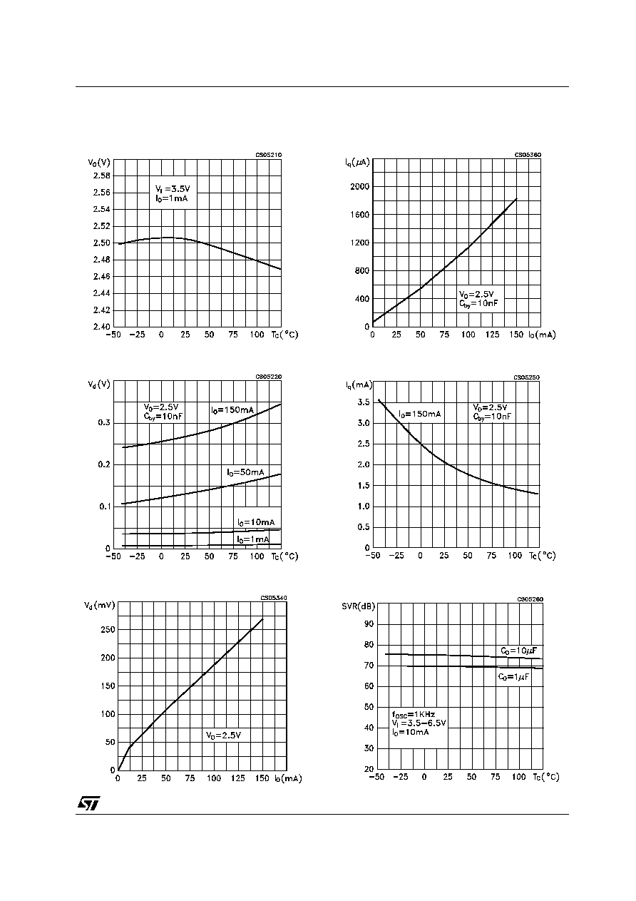
Figure 1 : Output Voltage vs Temperature
Figure 2 : Dropout Voltage vs Temperature
Figure 3 : Dropout Voltage vs Output Current
Figure 4 : Quiescent Current vs Load Current
Figure 5 : Quiescent Current vs Temperature
Figure 6 : Supply Voltage Rejection vs
Temperature
LD2985 SERIES
8/13
Figure 7 : Supply Voltage Rejection vs Output
Current
Figure 8 : Supply Voltage Rejection vs Output
Current
Figure 9 : Supply Voltage Rejection vs
Frequency
Figure 10 : Supply Voltage Rejection vs
Frequency
Figure 11 : Line Transient
Figure 12 : Line Transient
V
O
=2.5V, I
O
= 50mA, no C
I
, C
O
=4.7
µ
F, t
r
=t
f
=2ns
V
O
=2.5V, I
O
= 50mA, no C
I
, C
O
=4.7
µ
F, t
r
=t
f
=1
µ
s
LD2985 SERIES
9/13
Figure 13 : Load Transient
Figure 14 : Load Transient
EXTERNAL CAPACITORS
Like any low-dropout regulator, the LD2985 requires external capacitors for regulator stability. This
capacitor must be selected to meet the requirements of minimum capacitance and equivalent series
resistance. We suggest to solder input and output capacitors as close as possible to the relative pins.
INPUT CAPACITOR
An input capacitor whose value is 1µF is required with the LD2985 (amount of capacitance can be
increased without limit). This capacitor must be located a distance of not more than 0.5" from the input pin
of the device and returned to a clean analog ground. Any good quality ceramic, tantalum or film capacitors
can be used for this capacitor.
OUTPUT CAPACITOR
The LD2985 is designed specifically to work with ceramic output capacitors. It may also be possible to use
Tantalum capacitors, but these are not as attractive for reasons of size and cost. By the way, the output
capacitor must meet both the requirement for minimum amount of capacitance and E.S.R. (equivalent
series resistance) value. Due to the different loop gain, the stability improves for higher output versions
and so the suggested minimum output capacitor value, if low E.S.R. ceramic type is used, is 1µF for
output voltages equal or major than 3.8V, 2.2µF for V
O
going from 1.8 to 3.3V, and 3.3µF for the other
versions. However, if an output capacitor lower than the suggested one is used, it's possible to make
stable the regulator adding a resistor in series to the capacitor.
IMPORTANT:
The output capacitor must maintain its ESR in the stable region over the full operating temperature to
assure stability. Also, capacitor tolerance and variation with temperature must be considered to assure
the minimum amount of capacitance is provided at all times. This capacitor should be located not more
than 0.5" from the output pin of the device and returned to a clean analog ground.
INHIBIT INPUT OPERATION
The inhibit pin can be used to turn OFF the regulator when pulled low, so drastically reducing the current
consumption down to less than 1µA. When the inhibit feature is not used, this pin must be tied to V
I
to
keep the regulator output ON at all times. To assure proper operation, the signal source used to drive the
inhibit pin must be able to swing above and below the specified thresholds listed in the electrical
characteristics section under V
IH
V
IL
. Any slew rate can be used to drive the inhibit.
V
O
=2.5V, I
O
=0 to 50mA, no C
I
, C
O
=10
µ
F, t
s
=t
f
=2ns
V
O
=2.5V, I
O
=0 to 50mA, no C
I
, C
O
=4.7
µ
F, t
s
=t
f
=2ns
LD2985 SERIES
10/13
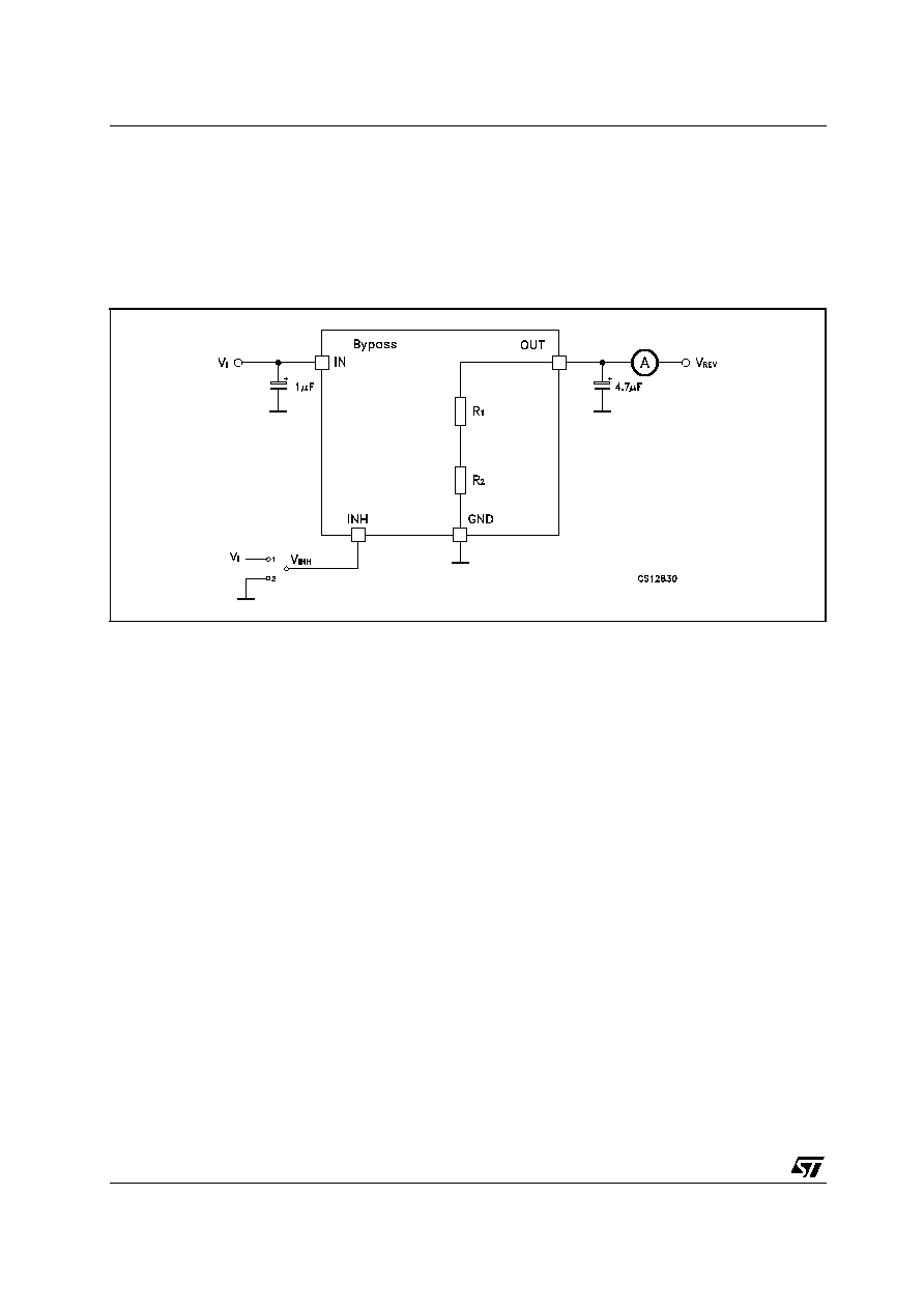
REVERSE CURRENT
The power transistor used in the LD2985 has not an inherent diode connected between the regulator input
and output. If the output is forced above the input, no current will flow from the output to the input across
the series pass transistor. When a V
REV
voltage is applied on the output, the reverse current measured
flows to the GND across the two feedback resistors. This current typical value is 160µA. R
1
and R
2
resistors are implanted type; typical values are, respectively, 42.6 K
and 51.150 K
.
Figure 15 : Reverse Current Test Circuit
LD2985 SERIES
11/13
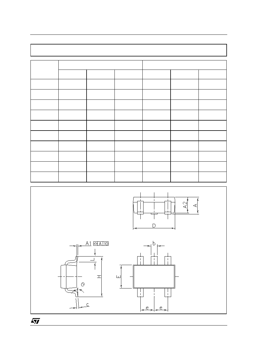
DIM.
mm.
mils
MIN.
TYP
MAX.
MIN.
TYP.
MAX.
A
0.90
1.45
35.4
57.1
A1
0.00
0.10
0.0
3.9
A2
0.90
1.30
35.4
51.2
b
0.35
0.50
13.7
19.7
C
0.09
0.20
3.5
7.8
D
2.80
3.00
110.2
118.1
E
1.50
1.75
59.0
68.8
e
0.95
37.4
H
2.60
3.00
102.3
118.1
L
0.10
0.60
3.9
23.6
SOT23-5L MECHANICAL DATA
7049676C
.
LD2985 SERIES
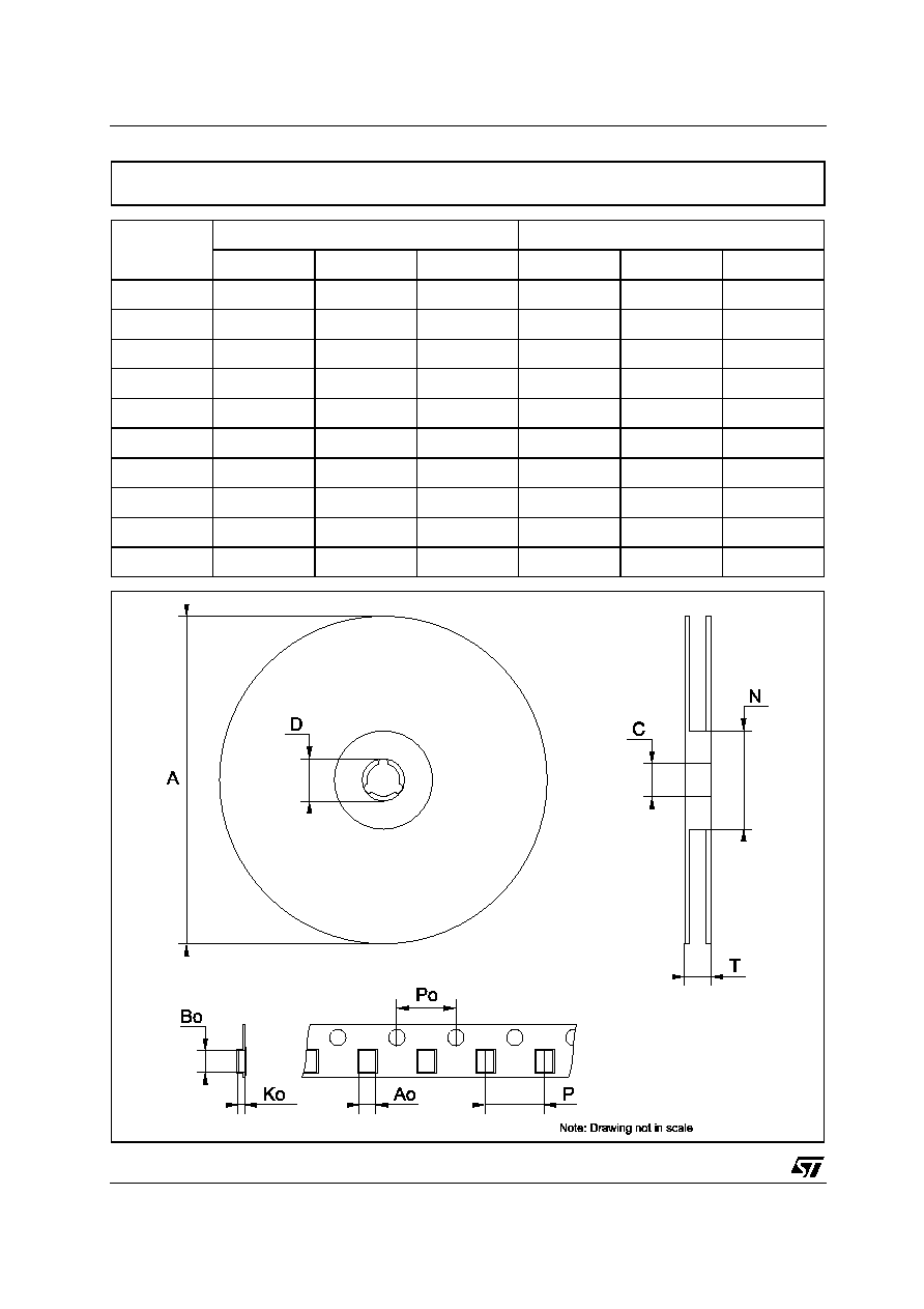
12/13
DIM.
mm.
inch
MIN.
TYP
MAX.
MIN.
TYP.
MAX.
A
180
7.086
C
12.8
13.0
13.2
0.504
0.512
0.519
D
20.2
0.795
N
60
2.362
T
14.4
0.567
Ao
3.13
3.23
3.33
0.123
0.127
0.131
Bo
3.07
3.17
3.27
0.120
0.124
0.128
Ko
1.27
1.37
1.47
0.050
0.054
0.0.58
Po
3.9
4.0
4.1
0.153
0.157
0.161
P
3.9
4.0
4.1
0.153
0.157
0.161
Tape & Reel SOT23-xL MECHANICAL DATA

LD2985 SERIES
13/13
Information furnished is believed to be accurate and reliable. However, STMicroelectronics assumes no responsibility for the
consequences of use of such information nor for any infringement of patents or other rights of third parties which may result from
its use. No license is granted by implication or otherwise under any patent or patent rights of STMicroelectronics. Specifications
mentioned in this publication are subject to change without notice. This publication supersedes and replaces all information
previously supplied. STMicroelectronics products are not authorized for use as critical components in life support devices or
systems without express written approval of STMicroelectronics.
© The ST logo is a registered trademark of STMicroelectronics
© 2003 STMicroelectronics - Printed in Italy - All Rights Reserved
STMicroelectronics GROUP OF COMPANIES
Australia - Brazil - Canada - China - Finland - France - Germany - Hong Kong - India - Israel - Italy - Japan - Malaysia - Malta - Morocco
Singapore - Spain - Sweden - Switzerland - United Kingdom - United States.
© http://www.st.com