
1/14
October 2004
s
INPUT VOLTAGE FROM 2.5V TO 6V
s
STABLE WITH LOW ESR CERAMIC
CAPACITORS
s
ULTRA LOW DROPOUT VOLTAGE (100mV
TYP. AT 150mA LOAD, 0.4mV TYP. AT 1mA
LOAD)
s
VERY LOW QUIESCENT CURRENT (85µA
TYP. AT NO LOAD, 170µA TYP. AT 150mA
LOAD; MAX 1.5µA IN OFF MODE)
s
GUARANTEED OUTPUT CURRENT UP TO
150mA
s
WIDE RANGE OF OUTPUT VOLTAGE: 1.2V;
1.22V; 1.25V; 1.35V; 1.5V; 1.8V; 2V; 2.1V;
2.2V; 2.4V; 2.5V; 2.6V; 2.7V; 2.8V; 2.85V;
2.9V; 3V; 3.1V; 3.2V; 3.3V; 4.7V; 5V
s
FAST TURN-ON TIME: TYP. 200µs [C
O
=1µF,
C
BYP
= 10nF AND I
O
=1mA]
s
LOGIC-CONTROLLED ELECTRONIC
SHUTDOWN
s
INTERNAL CURRENT AND THERMAL LIMIT
s
OUTPUT LOW NOISE VOLTAGE 30µVRMS
OVER 10Hz to 100KHz
s
S.V.R. OF 60dB AT 1KHz, 50dB AT 10KHz
s
TEMPERATURE RANGE: -40∞C TO 125∞C
DESCRIPTION
The LD3985 provides up to 150mA, from 2.5V to
6V input voltage.
The ultra low drop-voltage, low quiescent current
and low noise make it suitable for low power
applications and in battery powered systems.
Regulator ground current increases only slightly in
dropout, further prolonging the battery life. Power
supply rejection is better than 60 dB at low
frequencies and starts to roll off at 10KHz. High
power supply rejection is maintained down to low
input voltage levels common to battery operated
circuits. Shutdown Logic Control function is
available, this means that when the device is used
as local regulator, it is possible to put a part of the
board in standby, decreasing the total power
consumption. The LD3985 is designed to work
with low ESR ceramic capacitors. Typical
applications are in mobile phone and similar
battery powered wireless systems.
LD3985
SERIES
ULTRA LOW DROP-LOW NOISE BICMOS VOLTAGE
REGULATORS LOW ESR CAPACITORS COMPATIBLE
Figure 1: Schematic Diagram
Flip-Chip
(1.57x1.22)
TSOT23-5L
SOT23-5L
Rev. 8

LD3985 SERIES
2/14
Table 1: Absolute Maximum Ratings
Absolute Maximum Ratings are those values beyond which damage to the device may occur. Functional operation under these condition is
not implied.
(*) The input pin is able to withstand non repetitive spike of 6.5V for 200ms.
Table 2: Thermal Data
Table 3: Order Codes
(*) Available on request.
Symbol
Parameter
Value
Unit
V
I
DC Input Voltage
-0.3 to 6 (*)
V
V
O
DC Output Voltage
-0.3 to V
I
+0.3
V
V
INH
INHIBIT Input Voltage
-0.3 to V
I
+0.3
V
I
O
Output Current
Internally limited
P
D
Power Dissipation
Internally limited
T
STG
Storage Temperature Range
-65 to 150
∞C
T
OP
Operating Junction Temperature Range
-40 to 125
∞C
Symbol
Parameter
SOT23-5L/
TSOT23-5L
Flip-Chip
Unit
R
thj-case
Thermal Resistance Junction-case
81
∞C/W
R
thj-amb
Thermal Resistance Junction-ambient
255
170
∞C/W
SOT23-5L
TSOT23-5L
Flip-Chip
OUTPUT VOLTAGES
LD3985M12R (*)
LD3985G12R (*)
LD3985J12R (*)
1.20 V
LD3985M122R
LD3985G122R (*)
LD3985J122R
1.22 V
LD3985M125R (*)
LD3985G125R (*)
LD3985J125R
1.25 V
LD3985M135R (*)
LD3985G135R (*)
LD3985J135R
1.35 V
LD3985M15R
LD3985G15R (*)
LD3985J15R (*)
1.5 V
LD3985M18R
LD3985G18R
LD3985J18R
1.8 V
LD3985M20R (*)
LD3985G20R (*)
LD3985J20R (*)
2.0 V
LD3985M21R (*)
LD3985G21R (*)
LD3985J21R (*)
2.1 V
LD3985M22R (*)
LD3985G22R (*)
LD3985J22R (*)
2.2 V
LD3985M24R (*)
LD3985G24R (*)
LD3985J24R
2.4 V
LD3985M25R
LD3985G25R
LD3985J25R
2.5 V
LD3985M26R (*)
LD3985G26R (*)
LD3985J26R
2.6 V
LD3985M27R
LD3985G27R
LD3985J27R
2.7 V
LD3985M28R (*)
LD3985G28R (*)
LD3985J28R
2.8 V
LD3985M285R (*)
LD3985G285R (*)
LD3985J285R (*)
2.85 V
LD3985M29R
LD3985G29R
LD3985J29R
2.9 V
LD3985M30R (*)
LD3985G30R (*)
LD3985J30R
3.0 V
LD3985M31R (*)
LD3985G31R (*)
LD3985J31R
3.1 V
LD3985M32R (*)
LD3985G32R (*)
LD3985J32R (*)
3.2 V
LD3985M33R
LD3985G33R (*)
LD3985J33R
3.3 V
LD3985M44R (*)
LD3985G44R (*)
LD3985J44R (*)
4.4 V
LD3985M47R
LD3985G47R (*)
LD3985J47R
4.7 V
LD3985M48R (*)
LD3985G48R (*)
LD3985J48R
4.8 V
LD3985M49R (*)
LD3985G49R (*)
LD3985J49R (*)
4.9 V
LD3985M50R (*)
LD3985G50R (*)
LD3985J50R (*)
5.0 V
LD3985 SERIES
3/14
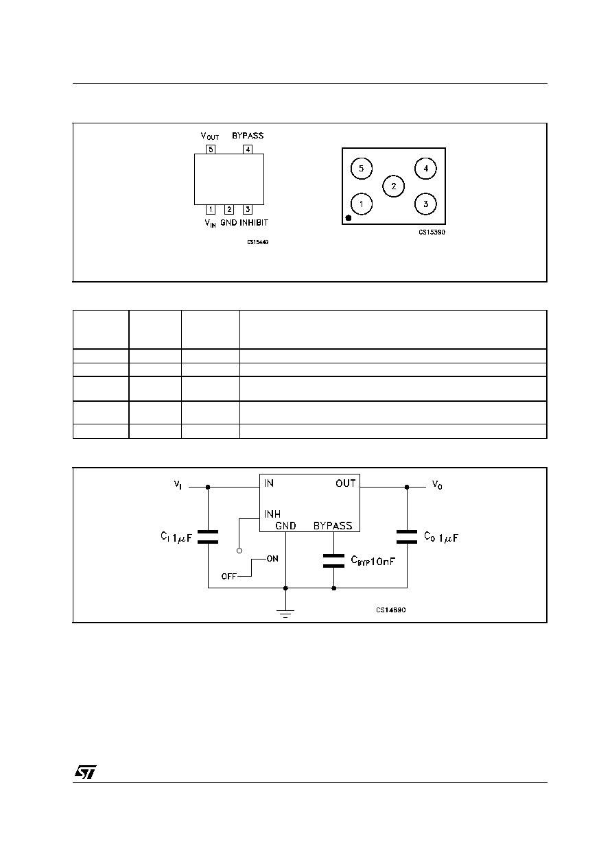
Figure 2: Connection Diagram (top view for SOT and TSOT, top through view for Flip-Chip)
Table 4: Pin Description
Figure 3: Typical Application Circuit
Pin N∞
SOT23-5L/
TSOT23-5L
Pin N∞
Flip-Chip
Symbol
Name and Function
1
4
V
I
Input Voltage of the LDO
2
2
GND
Common Ground
3
1
V
INH
Inhibit Input Voltage: ON MODE when V
INH
1.2V, OFF MODE when V
INH
0.4V (Do not leave floating, not internally pulled down/up)
4
5
BYPASS
Bypass Pin: Connect an external capacitor (usually 10nF) to minimize noise
voltage
5
3
V
O
Output Voltage of the LDO
TSOT23-5L/SOT23-5L
Flip-Chip
LD3985 SERIES
4/14
Table 5: Electrical Characteristics For LD3985 (T
j
= 25∞C, V
I
= V
O(NOM)
+0.5V, C
I
= 1
µ
F,
C
BYP
= 10nF, I
O
= 1mA, V
INH
= 1.4V, unless otherwise specified)
Symbol
Parameter
Test Conditions
Min.
Typ.
Max.
Unit
V
I
Operating Input Voltage
2.5
6
V
V
O
Output Voltage < 2.5V
I
O
= 1 mA
-50
50
mV
T
J
= -40 to 125∞C
-75
75
V
O
Output Voltage
2.5V
I
O
= 1 mA
-2
2
% of
V
O(NOM)
T
J
= -40 to 125∞C
-3
3
V
O
Line Regulation (Note 1)
V
I
= V
O(NOM)
+ 0.5 to 6 VT
J
= -40 to 125∞C
-0.1
0.1
%/V
V
O
= 4.7 to 5V
-0.19
0.19
V
O
Load Regulation
I
O
= 1 mA to 150mA
V
O
< 2.5V
T
J
= -40 to 125∞C
0.002
0.008
%/mA
V
O
Load Regulation
I
O
= 1 mA to 150mA
V
O
2.5V
T
J
= -40 to 125∞C (for Flip-Chip)
0.0004
0.002
%/mA
I
O
= 1 mA to 150mA, T
J
= -40 to 125∞C
(for SOT23-5L/TSOT23-5L), V
O
2.5V
0.0025
0.005
V
O
Output AC Line Regulation V
I
= V
O(NOM)
+ 1 V, I
O
= 150mA,
t
R
= t
F
= 30µs
1.5
mV
PP
I
Q
Quiescent Current
ON MODE: V
INH
= 1.2V
I
O
= 0
85
µA
I
O
= 0
T
J
= -40 to 125∞C
150
I
O
= 0 to 150mA
170
I
O
= 0 to 150mA
T
J
= -40 to 125∞C
250
OFF MODE: V
INH
= 0.4V
0.003
T
J
= -40 to 125∞C
1.5
V
DROP
Dropout Voltage (NOTE 1) I
O
= 1mA
0.4
mV
I
O
= 1mA
T
J
= -40 to 125∞C
2
I
O
= 50mA
20
I
O
= 50mA
T
J
= -40 to 125∞C
35
I
O
= 100mA
45
I
O
= 100mA
T
J
= -40 to 125∞C
70
I
O
= 150mA
60
I
O
= 150mA
T
J
= -40 to 125∞C
100
I
SC
Short Circuit Current
R
L
= 0
600
mA
SVR
Supply Voltage Rejection
V
I
= V
O(NOM)
+0.25V ±
V
RIPPLE
= 0.1V, I
O
= 50mA
V
O(NOM)
< 2.5V, V
I
= 2.55V
f = 1KHz
60
dB
f = 10KHz
50
I
O(PK)
Peak Output Current
V
O
V
O(NOM)
- 5%
300
550
mA
V
INH
Inhibit Input Logic Low
V
I
= 2.5V to 6V
T
J
= -40 to
125∞C
0.4
V
Inhibit Input Logic High
1.2
I
INH
Inhibit Input Current
V
INH
= 0.4V
V
I
= 6V
±1
nA
eN
Output Noise Voltage
B
W
= 10 Hz to 100 KHz
C
O
= 1
µ
F
30
µ
V
RMS
t
ON
Turn On Time (Note 4)
C
BYP
= 10 nF
100
250
µ
s
T
SHDN
Thermal Shutdown
Note 5
160
∞C
LD3985 SERIES
5/14
Note 1 ≠ For V
O(NOM)
< 2V, V
I
= 2.5V
Note 2 ≠ For V
O(NOM)
= 1.25V, V
I
= 2.5V
Note 3 ≠ Dropout voltage is the input-to-output voltage difference at which the output voltage is 100mV below its nominal value. This speci-
fication does not apply for input voltages below 2.5V.
Note 4 ≠ Turn-on time is time measured between the enable input just exceeding V
INH
High Value and the output voltage just reaching 95%
of its nominal value
Note 5 ≠ Typical thermal protection hysteresis is 20∞C
Note 6 - The minimum capacitor value is 1µF, anyway the LD3985 is still stable if the compensation capacitor has a 30% tolerance in all
temperature range.
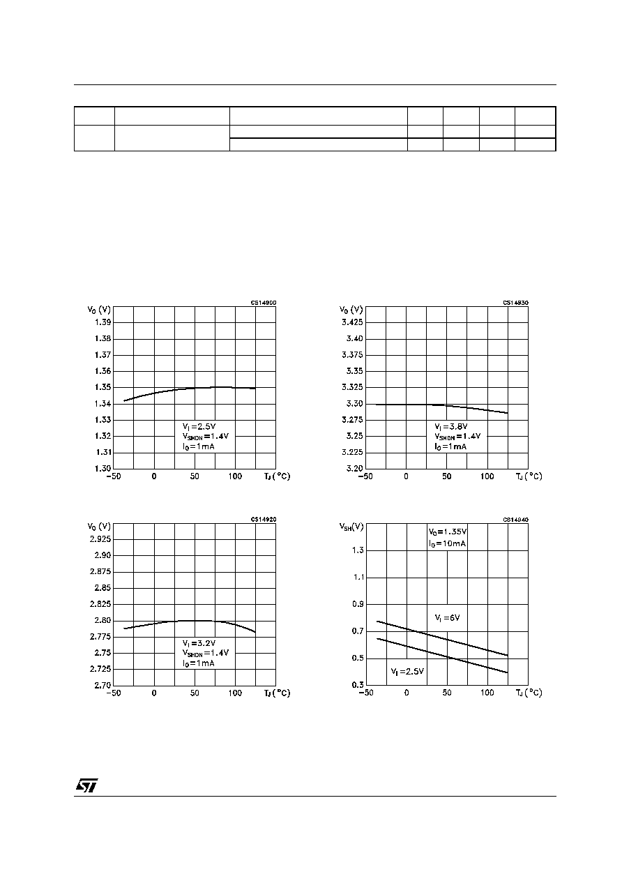
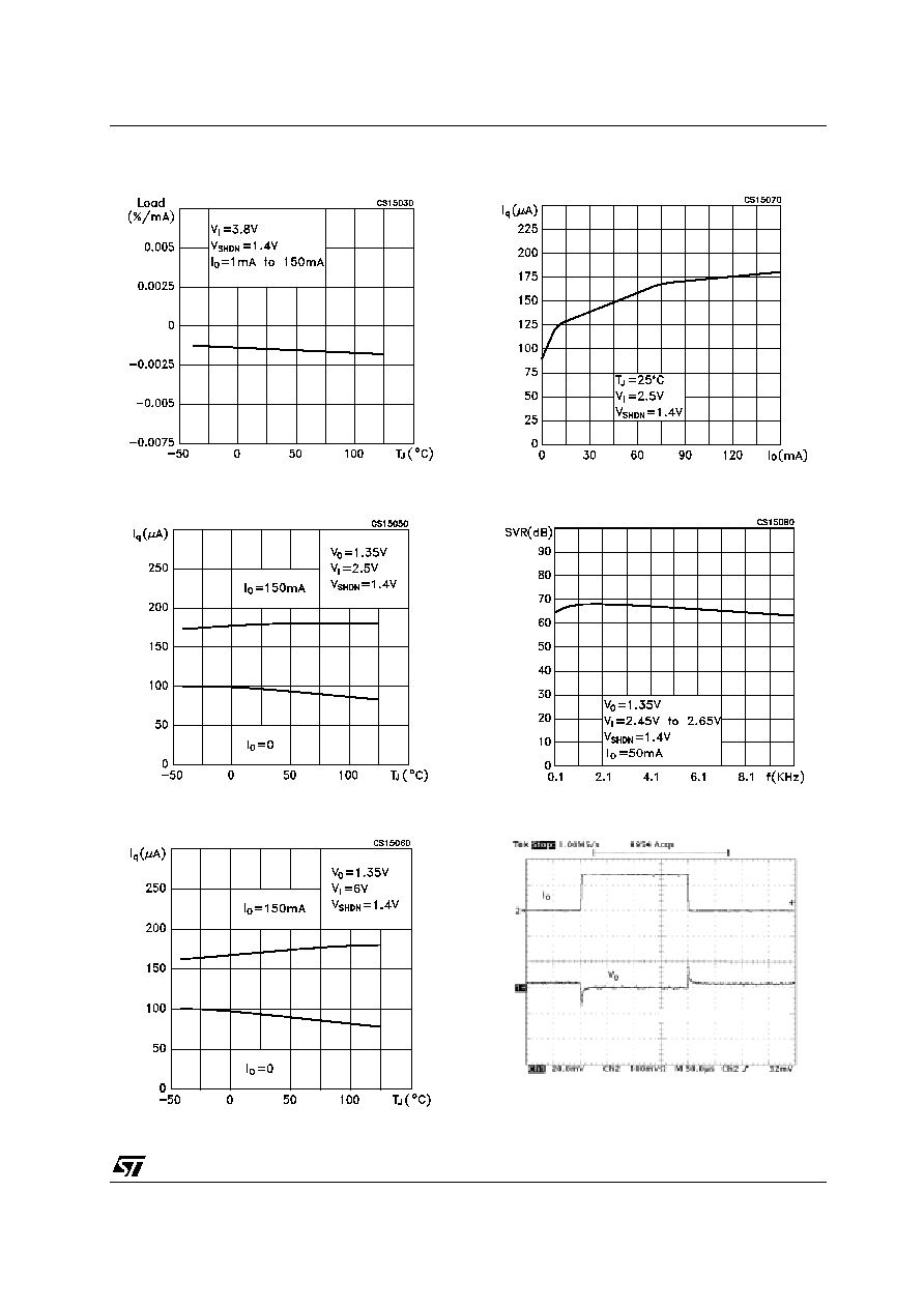
TYPICAL PERFORMANCE CHARACTERISTICS (T
j
= 25∞C, V
I
= V
O(NOM)
+0.5V, C
I
= C
O
= 1
µ
F,
C
BYP
= 1
0
nF, I
O
= 1mA, V
INH
= 1.4V, unless otherwise specified)
Figure 4: Output Voltage vs Temperature
Figure 5: Output Voltage vs Temperature
Figure 6: Output Voltage vs Temperature
Figure 7: Shutdown Voltage vs Temperature
C
O
Output Capacitor
Capacitance (Note 6)
1
22
µF
ESR
5
5000
m
Symbol
Parameter
Test Conditions
Min.
Typ.
Max.
Unit
LD3985 SERIES
6/14
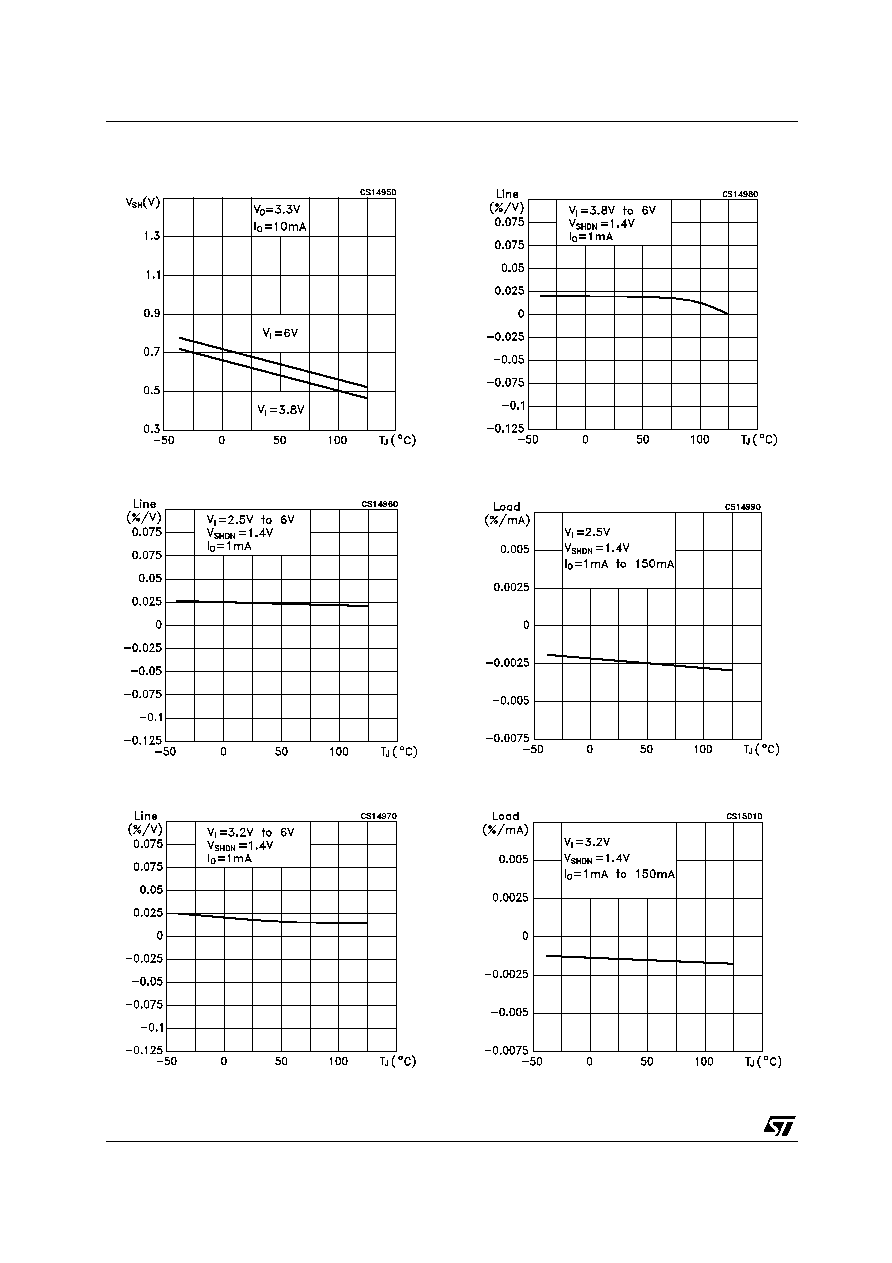
Figure 8: Shutdown Voltage vs Temperature
Figure 9: Line Regulation vs Temperature
Figure 10: Line Regulation vs Temperature
Figure 11: Line Regulation vs Temperature
Figure 12: Load Regulation vs Temperature
Figure 13: Load Regulation vs Temperature
LD3985 SERIES
7/14
Figure 14: Load Regulation vs Temperature
Figure 15: Quiescent Current vs Temperature
Figure 16: Quiescent Current vs Temperature
Figure 17: Quiescent Current vs Temperature
Figure 18: Supply Voltage Rejection vs
Frequency
Figure 19: Load Transient Response
V
I
= 3.2V, I
O
= 1 to 150mA, Rise-Fall time
= 1
µ
sec

LD3985 SERIES
8/14
Figure 20: Line Transient Response
Figure 21: START-UP
Figure 22: TURN-OFF
V
I
= 3.8V to 4.4V, T
J
= 25∞C, I
O
= 150mA, C
I
= C
O
= 1
µ
F (X7R),
C
BYP
= 10nF, Rise-Fall time
= 1
µ
sec, V
O
= 2.7V
V
I
= 3.3V, I
O
= 1mA, C
I
= C
O
= 1
µ
F (cer), C
BYP
= 10nF, T
r
= 20ns,
V
O
= 2.8V
V
I
= 3.3V, I
O
= 1mA, C
I
= C
O
= 1
µ
F (cer), C
BYP
= 10nF, T
f
= 20ns,
V
O
= 2.8V

LD3985 SERIES
9/14
DIM.
mm.
mils
MIN.
TYP
MAX.
MIN.
TYP.
MAX.
A
0.90
1.45
35.4
57.1
A1
0.00
0.10
0.0
3.9
A2
0.90
1.30
35.4
51.2
b
0.35
0.50
13.7
19.7
C
0.09
0.20
3.5
7.8
D
2.80
3.00
110.2
118.1
E
1.50
1.75
59.0
68.8
e
0.95
37.4
H
2.60
3.00
102.3
118.1
L
0.10
0.60
3.9
23.6
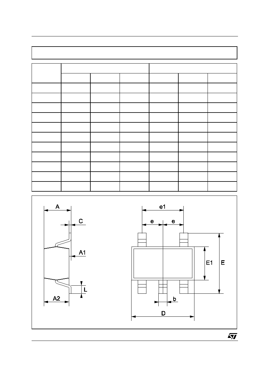
SOT23-5L MECHANICAL DATA
7049676C
.
LD3985 SERIES
10/14
DIM.
mm.
mils
MIN.
TYP
MAX.
MIN.
TYP.
MAX.
A
1.1
43.3
A1
0
0.1
3.9
A2
0.7
1.0
27.6
39.4
b
0.3
0.5
11.8
19.7
C
0.08
0.2
3.1
7.9
D
2.9
114.2
E
2.8
110.2
E1
1.6
63.0
e
0.95
37.4
e1
1.9
74.8
L
0.3
0.6
11.8
23.6
TSOT23-5L MECHANICAL DATA
7282780B

LD3985 SERIES
11/14
DIM.
mm.
mils
MIN.
TYP
MAX.
MIN.
TYP.
MAX.
A
0.835
0.9
0.965
32.874
35.433
37.992
A1
0.21
0.25
0.29
8.268
9.843
11.417
A2
0.625
0.65
0.675
24.606
25.591
26.575
b
0.265
0.315
0.365
10.433
12.402
14.370
D
1.510
1.540
1.570
59.449
60.630
61.811
E
1.16
1.19
1.22
45.669
46.850
48.031
e
0.45
0.5
0.55
17.717
19.685
21.654
e1
0.816
0.866
0.916
32.126
34.094
36.063
f
0.345
13.583
f1
0.337
13.268
Flip-Chip5 MECHANICAL DATA
LD3985 SERIES
12/14
DIM.
mm.
inch
MIN.
TYP
MAX.
MIN.
TYP.
MAX.
A
180
7.086
C
12.8
13.0
13.2
0.504
0.512
0.519
D
20.2
0.795
N
60
2.362
T
14.4
0.567
Ao
3.13
3.23
3.33
0.123
0.127
0.131
Bo
3.07
3.17
3.27
0.120
0.124
0.128
Ko
1.27
1.37
1.47
0.050
0.054
0.0.58
Po
3.9
4.0
4.1
0.153
0.157
0.161
P
3.9
4.0
4.1
0.153
0.157
0.161
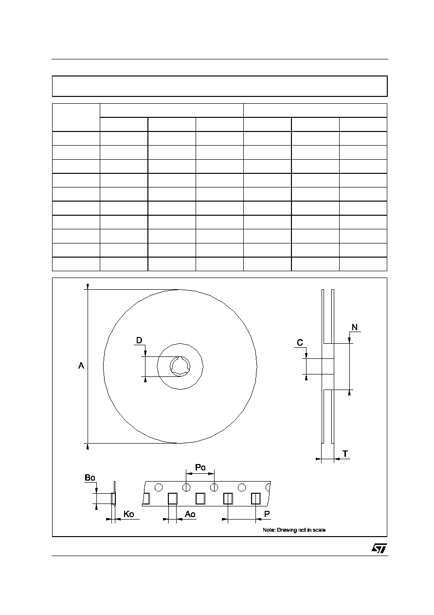
Tape & Reel SOT23-xL MECHANICAL DATA
LD3985 SERIES
13/14
Table 6: Revision History
Date
Revision
Description of Changes
07-May-2004
6
Part Number Status Changed on Table 3.
05-Oct-2004
7
t
ON
values are Changed on Table 5.
27-Oct-2004
8
Order Codes changed - Table 3.

LD3985 SERIES
14/14
Information furnished is believed to be accurate and reliable. However, STMicroelectronics assumes no responsibility for the consequences
of use of such information nor for any infringement of patents or other rights of third parties which may result from its use. No license is granted
by implication or otherwise under any patent or patent rights of STMicroelectronics. Specifications mentioned in this publication are subject
to change without notice. This publication supersedes and replaces all information previously supplied. STMicroelectronics products are not
authorized for use as critical components in life support devices or systems without express written approval of STMicroelectronics.
The ST logo is a registered trademark of STMicroelectronics
All other names are the property of their respective owners
© 2004 STMicroelectronics - All Rights Reserved
STMicroelectronics group of companies
Australia - Belgium - Brazil - Canada - China - Czech Republic - Finland - France - Germany - Hong Kong - India - Israel - Italy - Japan -
Malaysia - Malta - Morocco - Singapore - Spain - Sweden - Switzerland - United Kingdom - United States of America
www.st.com