
1/12
July 2003
s
INPUT VOLTAGE FROM 2.5V TO 6V
s
STABLE WITH LOW ESR CERAMIC
CAPACITORS
s
ULTRA LOW DROPOUT VOLTAGE (100mV
TYP. AT 150mA LOAD, 0.4mV TYP. AT 1mA
LOAD)
s
VERY LOW QUIESCENT CURRENT (85µA
TYP. AT NO LOAD, 170µA TYP. AT 150mA
LOAD; MAX 1.5µA IN OFF MODE)
s
GUARANTEED OUTPUT CURRENT UP TO
150mA
s
WIDE RANGE OF OUTPUT VOLTAGE:
1.25V; 1.35; 1.5; 1.8V; 2V; 2.1V; 2.2V; 2.4V;
2.5V; 2.6V; 2.7V; 2.8V; 2.85V; 2.9V; 3V; 3.1V;
3.2V; 3.3V; 4.7V; 5V
s
FAST TURN-ON TIME: TYP. 200µs [C
O
=1µF,
C
BYP
= 10nF AND I
O
=1mA]
s
LOGIC-CONTROLLED ELECTRONIC
SHUTDOWN
s
INTERNAL CURRENT AND THERMAL LIMIT
s
OUTPUT LOW NOISE VOLTAGE 30µVRMS
OVER 10Hz to 100KHz
s
S.V.R. OF 60dB AT 1KHz, 50dB AT 10KHz
s
TEMPERATURE RANGE: -40∞C TO 125∞C
DESCRIPTION
The LD3985 provides up to 150mA, from 2.5V to
6V input voltage.
The ultra low drop-voltage, low quiescent current
and low noise make it suitable for low power
applications and in battery powered systems.
Regulator ground current increases only slightly in
dropout, further prolonging the battery life. Power
supply rejection is better than 60 dB at low
frequencies and starts to roll off at 10KHz. High
power supply rejection is maintained down to low
input voltage levels common to battery operated
circuits. Shutdown Logic Control function is
available, this means that when the device is used
as local regulator, it is possible to put a part of the
board in standby, decreasing the total power
consumption. The LD3985 is designed to work
with
low
ESR
ceramic
capacitors.
Typical
applications are in mobile phone and similar
battery powered wireless systems.
LD3985
SERIES
ULTRA LOW DROP-LOW NOISE BICMOS VOLTAGE
REGULATORS LOW ESR CAPACITORS COMPATIBLE
SCHEMATIC DIAGRAM
Flip-Chip
(1.57x1.22)
SOT23-5L
LD3985 SERIES
2/12
ABSOLUTE MAXIMUM RATINGS
Absolute Maximum Ratings are those values beyond which damage to the device may occur. Functional operation under these condition is
not implied.
(*) The input pin is able to withstand non repetitive spike of 6.5V for 200ms.
THERMAL DATA
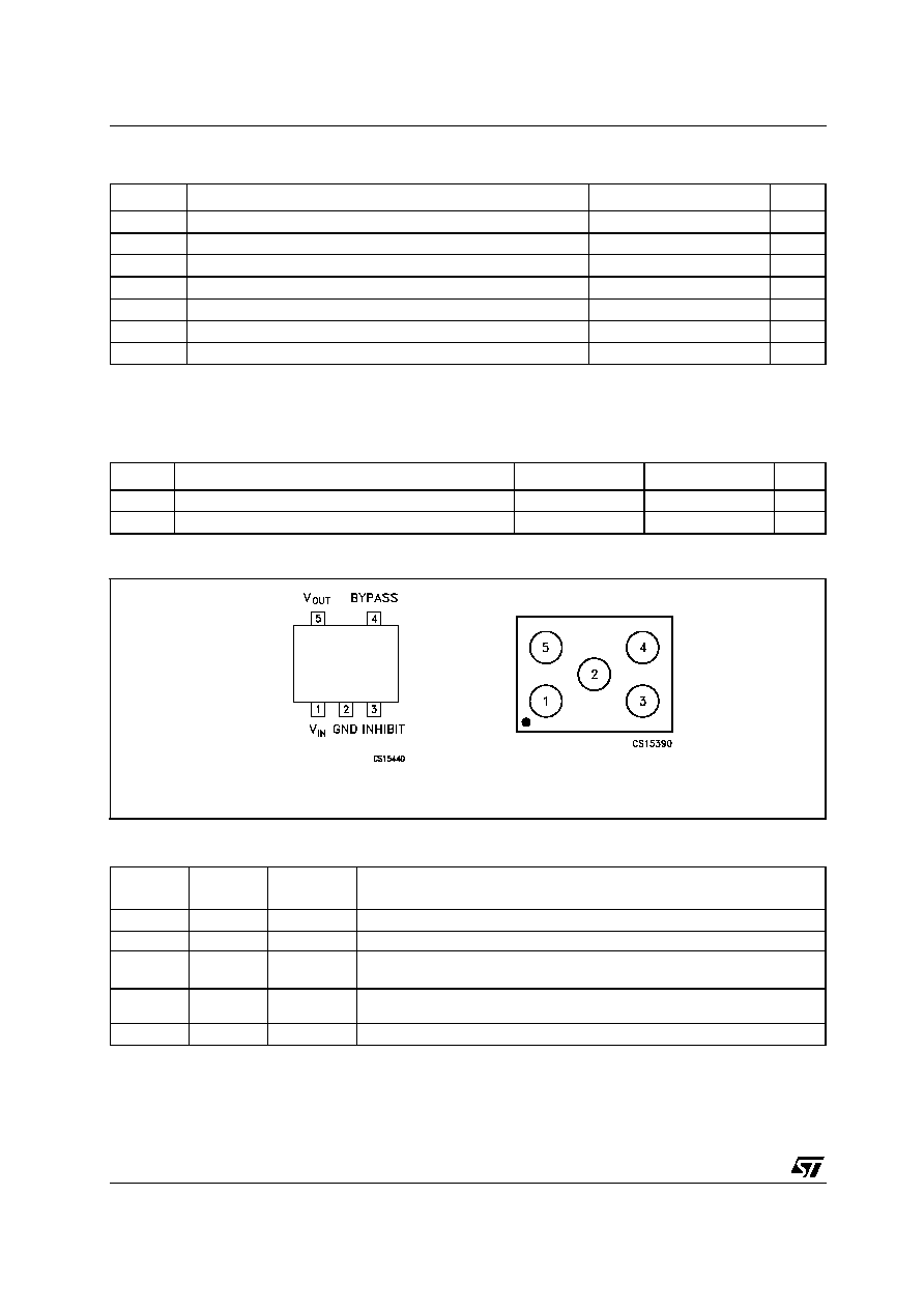
CONNECTION DIAGRAM (top view for SOT, top through view for Flip-Chip)
PIN DESCRIPTION
Symbol
Parameter
Value
Unit
V
I
DC Input Voltage
-0.3 to 6 (*)
V
V
O
DC Output Voltage
-0.3 to V
I
+0.3
V
V
INH
INHIBIT Input Voltage
-0.3 to V
I
+0.3
V
I
O
Output Current
Internally limited
P
D
Power Dissipation
Internally limited
T
STG
Storage Temperature Range
-65 to 150
∞C
T
OP
Operating Junction Temperature Range
-40 to 125
∞C
Symbol
Parameter
SOT23-5L
Flip-Chip
Unit
R
thj-case
Thermal Resistance Junction-case
81
∞C/W
R
thj-amb
Thermal Resistance Junction-ambient
255
170
∞C/W
Pin N∞
SOT23-5L
Pin N∞
Flip-Chip
Symbol
Name and Function
1
4
V
I
Input Voltage of the LDO
2
2
GND
Common Ground
3
1
V
INH
Inhibit Input Voltage: ON MODE when V
INH
1.2V, OFF MODE when V
INH
0.4V (Do not leave floating, not internally pulled down/up)
4
5
BYPASS
Bypass Pin: Connect an external capacitor (usually 10nF) to minimize noise
voltage
5
3
V
O
Output Voltage of the LDO
SOT23-5L
Flip-Chip

LD3985 SERIES
3/12
ORDERING CODES
TYPICAL APPLICATION CIRCUIT
SOT23-5L
Flip-Chip
OUTPUT VOLTAGES
LD3985M125R
LD3985J125R
1.25 V
LD3985M135R
LD3985J135R
1.35 V
LD3985M15R
LD3985J15R
1.5 V
LD3985M18R
LD3985J18R
1.8 V
LD3985M20R
LD3985J20R
2.0 V
LD3985M21R
LD3985J21R
2.1 V
LD3985M22R
LD3985J22R
2.2 V
LD3985M24R
LD3985J24R
2.4 V
LD3985M25R
LD3985J25R
2.5 V
LD3985M26R
LD3985J26R
2.6 V
LD3985M27R
LD3985J27R
2.7 V
LD3985M28R
LD3985J28R
2.8 V
LD3985M285R
LD3985J285R
2.85 V
LD3985M29R
LD3985J29R
2.9 V
LD3985M30R
LD3985J30R
3.0 V
LD3985M31R
LD3985J31R
3.1 V
LD3985M32R
LD3985J32R
3.2 V
LD3985M33R
LD3985J33R
3.3 V
LD3985M47R
LD3985J47R
4.7 V
LD3985M48R
LD3985J48R
4.8 V
LD3985M49R
LD3985J49R
4.9 V
LD3985M50R
LD3985J50R
5.0 V
LD3985 SERIES
4/12
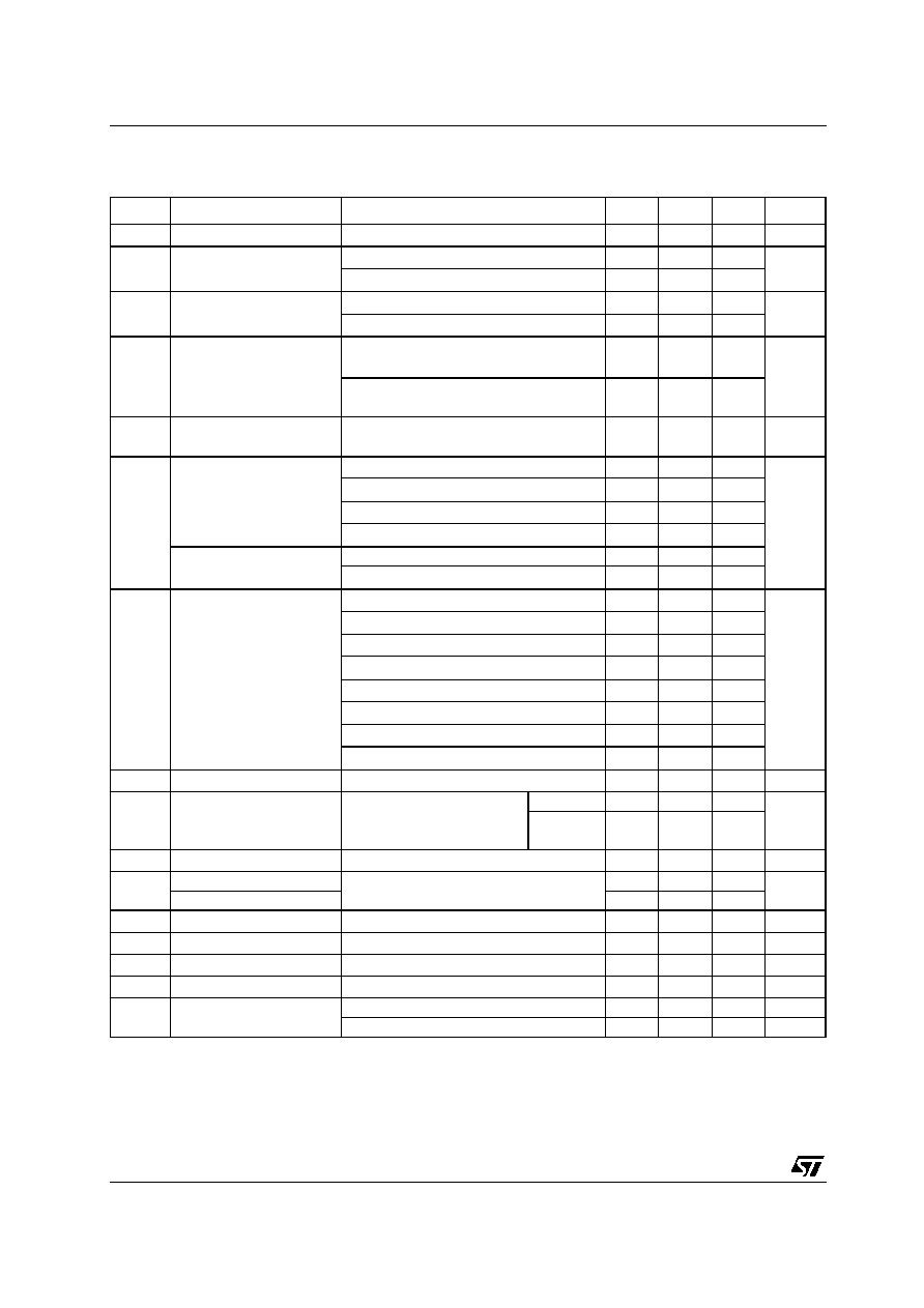
ELECTRICAL CHARACTERISTICS FOR LD3985 (T
j
= 25∞C, V
I
= V
O(NOM)
+0.5V, C
I
= 1
µ
F,
C
BYP
= 10nF, I
O
= 1mA, V
INH
= 1.4V, unless otherwise specified)
Note 1 ≠ For V
O(NOM)
< 2V, V
I
= 2.5V
Note 2 ≠ For V
O(NOM)
= 1.25V, V
I
= 2.5V
Note 3 ≠ Dropout voltage is the input-to-output voltage difference at which the output voltage is 100mV below its nominal value. This speci-
fication does not apply for input voltages below 2.5V.
Note 4 ≠ Turn-on time is time measured between the enable input just exceeding V
INH
High Value and the output voltage just reaching 95%
of its nominal value
Note 5 ≠ Typical thermal protection hysteresis is 20∞C
Note 6 - The minimum capacitor value is 1µF, anyway the LD3985 is still stable if the compensation capacitor has a 30% tolerance in all
temperature range.
Symbol
Parameter
Test Conditions
Min.
Typ.
Max.
Unit
V
I
Operating Input Voltage
2.5
6
V
V
O
Output Voltage
I
O
= 1 mA
-2
2
% of
V
O(NOM)
T
J
= -40 to 125
∞C
-3
3
V
O
Line Regulation (Note 1)
V
I
= V
O(NOM)
+ 0.5 to 6 VT
J
= -40 to 125
∞C
-0.1
0.1
%/V
V
O
= 4.7 to 5V
-0.19
0.19
V
O
Load Regulation
I
O
= 1 mA to 150mA (for Flip Chip)
T
J
= -40 to 125
∞C
0.0004
0.002
%/mA
I
O
= 1 mA to 150mA, T
J
= -40 to 125
∞C
(for SOT23-5L)
0.0025
0.005
V
O
Output AC Line Regulation V
I
= V
O(NOM)
+ 1 V, I
O
= 150mA,
t
R
= t
F
= 30µs
1.5
mV
PP
I
Q
Quiescent Current
ON MODE: V
INH
= 1.2V
I
O
= 0
85
µA
I
O
= 0
T
J
= -40 to 125
∞C
150
I
O
= 0 to 150mA
170
I
O
= 0 to 150mA
T
J
= -40 to 125
∞C
250
OFF MODE: V
INH
= 0.4V
0.003
T
J
= -40 to 125
∞C
1.5
V
DROP
Dropout Voltage (NOTE 1) I
O
= 1mA
0.4
mV
I
O
= 1mA
T
J
= -40 to 125
∞C
2
I
O
= 50mA
20
I
O
= 50mA
T
J
= -40 to 125
∞C
35
I
O
= 100mA
45
I
O
= 100mA
T
J
= -40 to 125
∞C
70
I
O
= 150mA
60
I
O
= 150mA
T
J
= -40 to 125
∞C
100
I
SC
Short Circuit Current
R
L
= 0
600
mA
SVR
Supply Voltage Rejection
V
I
= V
O(NOM)
+0.25V ±
V
RIPPLE
= 0.1V,
I
O
= 50mA
V
O(NOM)
< 2.5V,
V
I
= 2.55V
f = 1KHz
60
dB
f = 10KHz
50
I
O(PK)
Peak Output Current
V
O
V
O(NOM)
- 5%
300
550
mA
V
INH
Inhibit Input Logic Low
V
I
= 2.5V to 6V
T
J
= -40 to 125
∞C
0.4
V
Inhibit Input Logic High
1.2
I
INH
Inhibit Input Current
V
INH
= 0.4V
V
I
= 6V
±1
nA
eN
Output Noise Voltage
B
W
= 10 Hz to 100 KHz
C
O
= 1
µ
F
30
µ
V
RMS
t
ON
Turn On Time (Note 4)
C
BYP
= 10 nF
200
µ
s
T
SHDN
Thermal Shutdown
Note 5
160
∞C
C
O
Output Capacitor
Capacitance (Note 6)
1
22
µF
ESR
5
5000
m

LD3985 SERIES
5/12
TYPICAL PERFORMANCE CHARACTERISTICS (T
j
= 25∞C, V
I
= V
O(NOM)
+0.5V, C
I
= C
O
= 1
µ
F,
C
BYP
= 1
0
nF, I
O
= 1mA, V
INH
= 1.4V, unless otherwise specified)
Figure 1 : Output Voltage vs Temperature
Figure 2 : Output Voltage vs Temperature
Figure 3 : Output Voltage vs Temperature
Figure 4 : Shutdown Voltage vs Temperature
Figure 5 : Shutdown Voltage vs Temperature
Figure 6 : Line Regulation vs Temperature