
1/12
September 2005
s
INPUT VOLTAGE FROM 2.5V TO 6V
s
STABLE WITH LOW ESR CERAMIC
CAPACITORS
s
ULTRA LOW DROPOUT VOLTAGE (60mV
TYP. AT 150mA LOAD, 0.4mV TYP. AT 1mA
LOAD)
s
VERY LOW QUIESCENT CURRENT (155µA
TYP. AT NO LOAD, 290µA TYP. AT 150mA
LOAD; MAX 2µA IN OFF MODE)
s
GUARANTEED OUTPUT CURRENT UP TO
150mA FOR BOTH OUTPUTS
s
DUAL OUTPUT VOLTAGES
s
FAST TURN-ON TIME: TYP. 120µs (C
O
=1µF,
C
BYP
=10nF AND I
O
=1mA)
s
LOGIC-CONTROLLED ELECTRONIC
SHUTDOWN
s
INTERNAL CURRENT AND THERMAL LIMIT
s
OUTPUT LOW NOISE VOLTAGE 30µV
RMS
OVER 10Hz to 100KHz
s
S.V.R. OF 50dB AT 1KHz, 40dB AT 10KHz
s
TEMPERATURE RANGE: -40∞C TO 125∞C
DESCRIPTION
The LD3986 provides up to 150mA at each output,
from 2.5V to 6V input voltage. The ultra low
drop-voltage, low quiescent current and low noise
make it suitable for low power applications and in
battery powered systems. Regulator ground
current increases only slightly in dropout, further
prolonging the battery life. Power supply rejection
is 50 dB at 1KHz and 40 dB at 10KHz. High power
supply rejection is maintained down to low input
voltage levels common to battery operated
circuits. Shutdown Logic Control function is
available for each output, this means that when
the device is used as local regulator, it is possible
to put a part of the board in standby, decreasing
the total power consumption. The LD3986 is
designed to work with low ESR ceramic
capacitors. Typical applications are in mobile
phone and similar battery powered wireless
systems.
LD3986
SERIES
DUAL ULTRA LOW DROP-LOW NOISE BICMOS VOLTAGE
REG. FOR USE WITH VERY LOW ESR OUT. CAPACITORS
Figure 1: Schematic Diagram
Flip-Chip
Rev. 3
LD3986 SERIES
2/12
Table 1: Order Codes
(*) Available on Request.
Table 2: Absolute Maximum Ratings
Absolute Maximum Ratings are those values beyond which damage to the device may occur. Functional operation under these condition is
not implied.
Table 3: Thermal Data
Flip-Chip
Flip-Chip (Lead Free)
1 OUTPUT VOLTAGES
2 OUTPUT VOLTAGES
LD3986J122R-E
1.22 V
1.22 V
LD3986J12248R
LD3986J12248R-E
1.22 V
4.8 V
LD3986J1828R-E
1.8 V
2.8 V
LD3986J2528R-E (*)
2.5 V
2.8 V
LD3986J28R-E
2.8 V
2.8 V
LD3986J285R
LD3986J285R-E
2.85 V
2.85 V
LD3986J29R-E (*)
2.9 V
2.9 V
LD3986J30R-E (*)
3.0 V
3.0 V
LD3986J2830R-E (*)
2.8 V
3.0 V
LD3986J3133R-E (*)
3.1 V
3.3 V
LD3986J33R-E
3.3 V
3.3 V
Symbol
Parameter
Value
Unit
V
I
DC Input Voltage
-0.3 to 6
V
V
O1,2
DC Output Voltage
-0.3 to V
I
+0.3
V
V
EN1,2
ENABLE Input Voltage
-0.3 to V
I
+0.3
V
I
O
Output Current
Internally limited
P
D
Power Dissipation
Internally limited
T
STG
Storage Temperature Range
-65 to 150
∞C
T
OP
Operating Junction Temperature Range
-40 to 125
∞C
Symbol
Parameter
Flip-Chip
Unit
R
thj-amb
Thermal Resistance Junction-Ambient
120
∞C/W
LD3986 SERIES
3/12
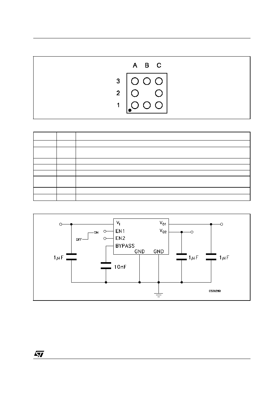
Figure 2: Pin Connection (top through view)
Table 4: Pin Description
Figure 3: Typical Application Circuit
Symbol
Pin N∞
Name and Function
V
O2
A1
Output Voltage 2 of the dual LDO
EN2
B1
Enables voltage for output voltage 2: ON MODE when V
EN
1.4V, OFF MODE when V
EN
0.4V (Do not leave floating, not internally pulled down/up)
BYPASS
C1
Bypass Pin: Connect an external capacitor (usually 10nF) to minimize noise voltage
GND
C2
Common Ground
GND
C3
Common Ground
EN1
B3
Enables voltage for output voltage 1: ON MODE when V
EN
1.4V, OFF MODE when V
EN
0.4V (Do not leave floating, not internally pulled down/up)
V
O1
A3
Output Voltage 1 of the dual LDO
V
I
A2
Input Voltage for both LDO

LD3986 SERIES
4/12
Table 5: Electrical Characteristics For LD3986 (T
j
= 25∞C, V
I
= V
O(NOM)
+0.5V, C
I
= C
O
=1
µ
F,
C
BYP
= 10nF, I
O
= 1mA, V
EN
= 1.4V, unless otherwise specified)
Symbol
Parameter
Test Conditions
Min.
Typ.
Max.
Unit
V
I
Operating Input Voltage
2.5
6
V
V
O
Output Voltage Tolerance
I
O
= 1mA
-2.5
2.5
% of V
O
T
J
= -40 to 125∞C
-3
3
V
O
Line Regulation (Note 1)
V
I
= V
O(NOM)
+ 0.5 V to 6V
0.006
0.092
%/V
T
J
= -40 to 125∞C
0.128
V
O
Load Regulation
I
O
= 1 mA to 150mA
0.003
0.006
%/mA
T
J
= -40 to 125∞C
0.01
V
O
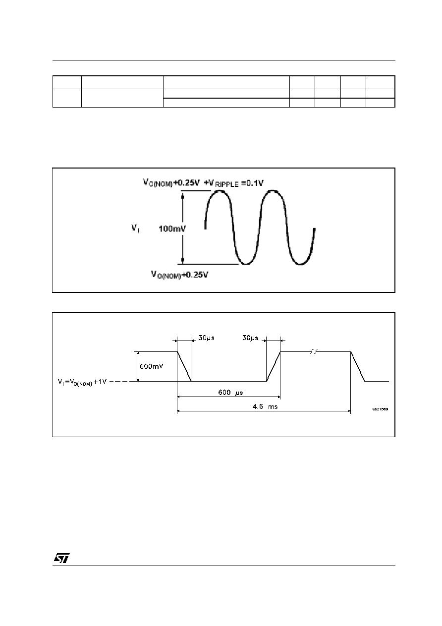
Output AC Line Regulation
(See fig. 5)
V
I
= V
O(NOM)
+ 1 V, I
O
= 150mA,
t
R
= t
F
= 30µs
1.5
mV
PP
I
Q
Quiescent Current
BOTH ON MODE:
V
EN
= 1.4V
I
O
= 0
150
µA
I
O
= 0
T
J
= -40 to 125∞C
200
I
O
= 0 to 150mA
290
I
O
= 0 to 150mA
T
J
= -40 to 125∞C
370
BOTH OFF MODE:
V
EN
= 0.4V
0.001
2
T
J
= -40 to 125∞C
4
ONE REGULATOR
ON MODE: V
EN
= 1.4V
I
O
= 0
95
I
O
= 0
T
J
= -40 to 125∞C
130
I
O
= 0 to 150mA
165
I
O
= 0 to 150mA
T
J
= -40 to 125∞C
220
V
DROP
Dropout Voltage (Note 2)
I
O
= 1mA
0.4
mV
I
O
= 1mA
T
J
= -40 to 125∞C
2
I
O
= 150mA
50
I
O
= 150mA
T
J
= -40 to 125∞C
100
SVR
Supply Voltage Rejection
(See fig. 4)
V
I
= V
O(NOM)
+0.25V ±
V
RIPPLE
= 0.1V, I
O
= 50mA
V
O(NOM)
< 2.5V, V
I
= 2.55V
f = 1KHz
50
dB
f = 10KHz
40
I
SC
Short Circuit Current
R
L
= 0
600
mA
I
O(PK)
Peak Output Current
V
O
V
O(NOM)
- 5%
300
550
mA
V
EN
Enable Input Logic Low
(Note 3)
V
I
= 2.5V to 6V
T
J
= -40 to 125∞C
0.4
V
Enable Input Logic High
(Note 3)
1.4
I
EN
Enable Input Current
V
EN
= 0.4V
V
I
= 6V
±10
nA
X
TALK
Crosstalk Rejection
I
LOAD1
= 150 mA at 1KHz rate
I
LOAD2
= 1 mA, V
O2
under test
40
µV
I
LOAD2
= 150 mA at 1KHz rate
I
LOAD1
= 1 mA, V
O1
under test
40
eN
Output Noise Voltage
B
W
= 10 Hz to 100 KHz
C
O
= 1
µ
F
30
µ
V
RMS
t
ON
Turn On Time (Note 4)
C
BYP
= 10 nF
50
µ
s
T
SHDN
Thermal Shutdown (Note
4)
(Note 3)
160
∞C
LD3986 SERIES
5/12
Note 1: For V
O
< 2V, V
I
=2.5V
Note 2: Dropout voltage is the input-to-output voltage difference at which the output voltage is 100mV below its nominal value. This specifi-
cation does not apply for input voltages below 2.5V.
Note 3: Enable pin must be driven with a T
R
= T
F
< 10ms
Note 4: Turn-on time is time measured between the enable input just exceeding V
INH
High Value and the output voltage just reaching 95%
of its nominal value
Note 5: Typical thermal protection hysteresis is 20∞C
Figure 4: SVR Input Voltage Test Signal
Figure 5: AC Line Regulation Input Voltage Test Signal
C
O
Output Capacitor
Capacitance
1
22
µF
ESR
0.005
5
Symbol
Parameter
Test Conditions
Min.
Typ.
Max.
Unit