
1/13
August 2004
s
OUTPUT CURRENT 1 UP TO 500mA
s
OUTPUT CURRENT 2 UP TO 1.0A
s
LOW DROPOUT VOLTAGE 1
(0.3V @ I
O
=500mA)
s
LOW DROPOUT VOLTAGE 2
(0.4V @ I
O
=1A)
s
VERY LOW SUPPLY CURRENT (TYP.50�A
IN OFF MODE, 1.6mA MAX IN ON MODE)
s
LOGIC-CONTROLLED ELECTRONIC
SHUTDOWN
s
OUTPUT VOLTAGE AVAILABILITY FOR
EACH REGULATOR: 1.8V, 2.5V, 3.3V
s
INTERNAL CURRENT AND THERMAL LIMIT
s
STABLE WITH LOW VALUE (MIN 4.7�F)
AND LOW E.S.R. OUTPUT CAPACITORS
s
SUPPLY VOLTAGE REJECTION: 70dB (TYP.)
s
TEMPERATURE RANGE (-40�C TO 125�C)
DESCRIPTION
The LDRxxyy is a Very Low Drop Dual Voltage
Regulator available in PPAK for the version
without inhibit and in SPAK-7L for the version with
the shutdown feature. The very low drop-voltage
(0.5V) and the very low supply current make it
particularly suitable for low noise and low power
applications such as PDA, MICRODRIVE and
other data storage applications while the used
high voltage technology makes this device
suitable for consumer applications such as
MONITORS AND SET-TOP-BOX. For each V
O
a
Shutdown Logic Control function is available (TTL
compatible) to decrease the total power
consumption.
LDRxxyy
VERY LOW DROP
DUAL VOLTAGE REGULATOR
+
-
+
-
START UP 1
BAND GAP 1
DRIVER 1
POWER 1
THERMAL 1
THERMAL 2
START UP 2
BAND GAP 2
DRIVER 2
POWER 2
V
O1
V
O2
I
NH2
I
NH1
V
I2
V
I1
ERROR
AMPLIFIER 1
ERROR
AMPLIFIER 2
Figure 1: Block Diagram
PPAK
SPAK-7L
Rev. 2

LDRxxyy
2/13
Table 1: Absolute Maximum Ratings
Absolute Maximum Rating are those values beyond which damage to the device may occur. Functional operation under these conditions is
not implied.
Table 2: Thermal Data
Figure 2: Connection Diagram (top view)
Table 3: Pin Description
Table 4: Order Codes
Symbol
Parameter
Value
Unit
V
I1
&
V
I2
DC Input Voltage
-0.3 to 15
V
INH
Shutdown Voltage
-0.3 to 15
V
I
O
Output Current
Internally Limited
P
TOT
Power Dissipation
Internally Limited
T
STG
Storage Temperature Range
-50 to +150
�C
T
A
Operating Ambient Temperature Range
-40 to +125
�C
Symbol
Parameter
PPAK
SPAK-7L
Unit
R
THJ-C
Junction to case thermal resistance
8
2
�C/W
Symbol
Pin N� for
PPAK
Pin N� for
SPAK-7L
Name and Function
GND
3
4
Ground pin
V
I1
2
2
Input 1 Supply Pin. Bypass with a 2.2�F capacitor to GND
V
I2
1
1
Input 2 Supply Pin. Bypass with a 2.2�F capacitor to GND
V
INH1
3
Enable 1 Pin. Internally connected to V
I1
in the PPAK version
V
INH2
5
Enable 2 Pin. Internally connected to V
I2
in the PPAK version
V
O1
4
6
Output 1 Pin. Bypass with a 4.7�F capacitor to GND Port
V
O2
5
7
Output 2 Pin. Bypass with a 4.7�F capacitor to GND Port
N.C.
Not Internally Connected
V
O1
V
O2
TYPE
PART NUMBERS
SPAK-7L
PPAK
1.8 V
2.5 V
LDR1825
LDR1825K7-R
LDR1825PT-R
1.8 V
3.3 V
LDR1833
LDR1833K7-R
LDR1833PT-R
2.5 V
1.8 V
LDR2518
LDR2518K7-R
LDR2518PT-R
2.5 V
3.3 V
LDR2533
LDR2533K7-R
LDR2533PT-R
3.3 V
1.8 V
LDR3318
LDR3318K7-R
LDR3318PT-R
3.3 V
2.5 V
LDR3325
LDR3325K7-R
LDR3325PT-R
SPAK-7L
PPAK

LDRxxyy
3/13
Table 5: Electrical Characteristics (V
I1
= V
O1
+2V, V
I2
= V
O2
+2V, V
INH1
= V
INH2
= 2.5V,
C
I1,2
= 2.2
�
F, C
O1,2
= 4.7
�
F, I
O1
= I
O2
= 10mA, T
A
= -40�C to 125�C, unless otherwise specified. Typical
values are referred at T
A
= 25�C)
(1): This test is not performed for V
O
<2.5V.
(2): Guaranteed by design, but not tested in production.
Figure 3: Typical Application Circuit
Symbol
Parameter
Test Conditions
Min.
Typ.
Max.
Unit
V
O1
Output Voltage 1
-5
V
NOM1
+5
%V
V
O2
Output Voltage 2
-5
V
NOM2
+5
%V
V
DROP1
Dropout Voltage 1
(1)
I
O1
= 500mA
0.3
0.7
V
V
DROP2
Dropout Voltage 2
(1)
I
O2
= 1A
0.4
0.8
V
V
O1
Line Regulation 1
V
I1
= V
O1
+2V to V
O1
+7V, I
O
= 250mA
15
30
mV
V
O2
Line Regulation 2
V
I2
= V
O2
+2V to V
O2
+7V, I
O
= 500mA
15
40
mV
V
O1
Load Regulation 1
V
I1
= V
O1
+2V, I
O1
= 10 to 500mA
10
mV
V
O2
Load Regulation 2
V
I2
= V
O2
+2V, I
O2
= 10mA to 1A
60
mV
I
STOT
Total Supply Current
I
O1
= I
O2
= NO LOAD
2
mA
I
S
1 Channel Supply Current
NO LOAD
1
mA
I
QMAX
Quiescent Current
I
O1
= 500mA, I
O2
= 1A
30
mA
I
SC1
Short Circuit Current 1
T
A
= 25�
500
800
mA
I
SC2
Short Circuit Current 2
T
A
= 25�
1
1.6
A
V
INH-H
Enable Voltage HIGH
2.4
V
V
INH-L
Enable Voltage LOW
0.8
V
I
INH
Enable Pin Current
V
INH
= 5V
6
�A
SVR
Supply Voltage Rejection
(2)
V
I1,2
= V
O1,2
+3V
�
1V, I
O1,2
= 10 mA,
f = 120Hz
70
dB
e
N
RMS Output Noise
(2)
Bandwidth of 10Hz to 100KHz
0.003
%V
O

LDRxxyy
4/13
TYPICAL CHARACTERISTICS (unless otherwise specified T
j
= 25�C)
Figure 4: Dropout Voltage (V
O1
) vs Temperature
Figure 5: Dropout Voltage (V
O2
) vs Temperature
Figure 6: Output Voltage (V
O1
) vs Temperature
Figure 7: Output Voltage (V
O2
) vs Temperature
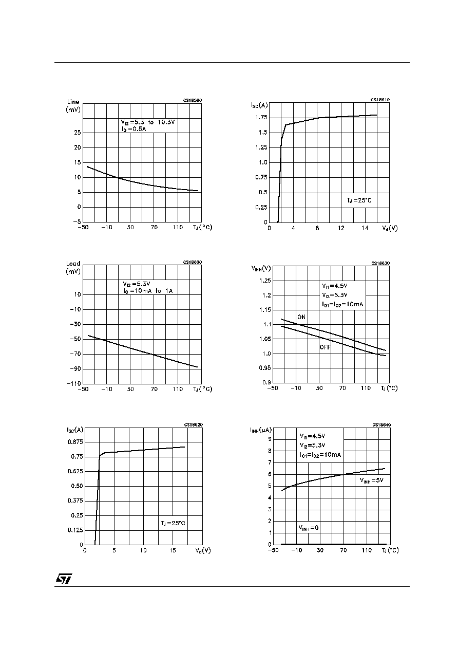
Figure 8: Line Regulation (V
O1
) vs Temperature
Figure 9: Load Regulation (V
O1
) vs Temperature
LDRxxyy
5/13
Figure 10: Line Regulation (V
O2
) vs Temperature
Figure 11: Load Regulation (V
O2
) vs
Temperature
Figure 12: Short Circuit Current (V
O1
) vs Drop
Voltage
Figure 13: Short Circuit Current (V
O2
) vs Drop
Voltage
Figure 14: Inhibit Voltage vs Temperature
Figure 15: One Channel Inhibit Current vs
Temperature