 | –≠–ª–µ–∫—Ç—Ä–æ–Ω–Ω—ã–π –∫–æ–º–ø–æ–Ω–µ–Ω—Ç: LE52AB | –°–∫–∞—á–∞—Ç—å:  PDF PDF  ZIP ZIP |
Document Outline
- Table 1: Absolute Maximum Ratings
- Table 2: Thermal Data
- Figure 1: Test Circuits
- Figure 2: Pin Connection (top view)
- Table 3: Ordering Codes
- Table 4: Electrical Characteristics For LE12AB (refer to the test circuits, Tj = 25�C, CI = 0.1 µ...
- Table 5: Electrical Characteristics For LE12C (refer to the test circuits, Tj = 25�C, CI = 0.1 µF...
- Table 6: Electrical Characteristics For LE15AB (refer to the test circuits, Tj = 25�C, CI = 0.1 µ...
- Table 7: Electrical Characteristics For LE15C (refer to the test circuits, Tj = 25�C, CI = 0.1 µF...
- Table 8: Electrical Characteristics For LE25AB (refer to the test circuits, Tj = 25�C, CI = 0.1 µ...
- Table 9: Electrical Characteristics For LE25C (refer to the test circuits, Tj = 25�C, CI = 0.1 µF...
- Table 10: Electrical Characteristics For LE27AB (refer to the test circuits, Tj = 25�C, CI = 0.1 ...
- Table 11: Electrical Characteristics For LE27C (refer to the test circuits, Tj = 25�C, CI = 0.1 µ...
- Table 12: Electrical Characteristics For LE30AB (refer to the test circuits, Tj = 25�C, CI = 0.1 ...
- Table 13: Electrical Characteristics For LE30C (refer to the test circuits, Tj = 25�C, CI = 0.1 µ...
- Table 14: Electrical Characteristics For LE33AB (refer to the test circuits, Tj = 25�C, CI = 0.1 ...
- Table 15: Electrical Characteristics For LE33C (refer to the test circuits, Tj = 25�C, CI = 0.1 µ...
- Table 16: Electrical Characteristics For LE35AB (refer to the test circuits, Tj = 25�C, CI = 0.1 ...
- Table 17: Electrical Characteristics For LE35C (refer to the test circuits, Tj = 25�C, CI = 0.1 µ...
- Table 18: Electrical Characteristics For LE40AB (refer to the test circuits, Tj = 25�C, CI = 0.1 ...
- Table 19: Electrical Characteristics For LE40C (refer to the test circuits, Tj = 25�C, CI = 0.1 µ...
- Table 20: Electrical Characteristics For LE45AB (refer to the test circuits, Tj = 25�C, CI = 0.1 ...
- Table 21: Electrical Characteristics For LE45C (refer to the test circuits, Tj = 25�C, CI = 0.1 µ...
- Table 22: Electrical Characteristics For LE47AB (refer to the test circuits, Tj = 25�C, CI = 0.1 ...
- Table 23: Electrical Characteristics For LE47C (refer to the test circuits, Tj = 25�C, CI = 0.1 µ...
- Table 24: Electrical Characteristics For LE50AB (refer to the test circuits, Tj = 25�C, CI = 0.1 ...
- Table 25: Electrical Characteristics For LE50C (refer to the test circuits, Tj = 25�C, CI = 0.1 µ...
- Table 26: Electrical Characteristics For LE52AB (refer to the test circuits, Tj = 25�C, CI = 0.1 ...
- Table 27: Electrical Characteristics For LE52C (refer to the test circuits, Tj = 25�C, CI = 0.1 µ...
- Table 28: Electrical Characteristics For LE55AB (refer to the test circuits, Tj = 25�C, CI = 0.1 ...
- Table 29: Electrical Characteristics For LE55C (refer to the test circuits, Tj = 25�C, CI = 0.1 µ...
- Table 30: Electrical Characteristics For LE60AB (refer to the test circuits, Tj = 25�C, CI = 0.1 ...
- Table 31: Electrical Characteristics For LE60C (refer to the test circuits, Tj = 25�C, CI = 0.1 µ...
- Table 32: Electrical Characteristics For LE80AB (refer to the test circuits, Tj = 25�C, CI = 0.1 ...
- Table 33: Electrical Characteristics For LE80C (refer to the test circuits, Tj = 25�C, CI = 0.1 µ...
- Table 34: Electrical Characteristics For LE120AB (refer to the test circuits, Tj = 25�C, CI = 0.1...
- Table 35: Electrical Characteristics For LE120C (refer to the test circuits, Tj = 25�C, CI = 0.1 ...
- Figure 3: Dropout Voltage vs Output Current
- Figure 4: Dropout Voltage vs Temperature
- Figure 5: Supply Current vs Temperature
- Figure 6: Supply Current vs Input Voltage
- Figure 7: Short Circuit Current vs Dropout Voltage
- Figure 8: S.V.R. vs Frequency
- Figure 9: Logic Controlled Precision 3.3/5.0V Selectable Output
- Figure 10: Sequential Multi-Output Supply
- Figure 11: Multiple Supply With ON/OFF Toggle Switch
- Figure 12: Basic Inhibit Functions
- Table 36: Revision History
1/27
July 2004
s
VERY LOW DROPOUT VOLTAGE (0.2V TYP)
s
VERY LOW QUIESCENT CURRENT (TYP.
50 µA IN OFF MODE, 0.5 mA IN ON MODE,
NO LOAD)
s
OUTPUT CURRENT UP TO 100 mA
s
OUTPUT VOLTAGES OF 1.25; 1.5; 2.5; 3;
3.3; 3.5; 4; 4.5; 4.7; 5; 5.2; 5.5; 6; 8V
s
INTERNAL CURRENT AND THERMAL LIMIT
s
ONLY 2.2 µF FOR STABILITY
s
AVAILABLE IN ± 1% (A) OR ± 2% (C)
SELECTION AT 25∞C
s
SUPPLY VOLTAGE REJECTION: 80db (TYP.)
s
TEMPERATURE RANGE: -40 TO 125 ∞C
DESCRIPTION
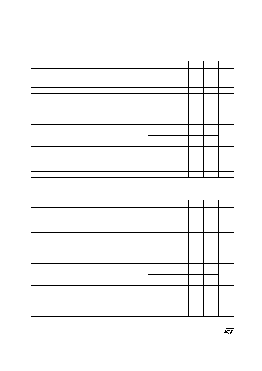
The LE00 regulator series are very Low Drop
regulators available in SO-8 and TO-92 packages
and in a wide range of output voltages.
The very Low Drop voltage (0.2V) and the very
low quiescent current make them particularly
suitable for Low Noise Low Power applications
and specially in battery powered systems.
They are pin to pin compatible with the older
L78L00 series. Furthermore in the 8 pin
configuration (SO-8) they employ a Shutdown
Logic Control (pin 5, TTL compatible). This means
that when the device is used as a local regulator,
it's possible to put in stand by a part of the board
even more decreasing the total power
consumption. In the three terminal configuration
(TO-92) the device is even in ON STATE,
maintaining the same electrical performances. It
needs only 2.2µF capacitor for stability allowing
room and cost saving effect.
LE00AB/C
SERIES
VERY LOW DROP
VOLTAGE REGULATORS WITH INHIBIT
SCHEMATIC DIAGRAM
SO-8
TO-92
Rev. 6

LE00AB/C SERIES
2/27
Table 1: Absolute Maximum Ratings
(*) Our SO-8 package used for Voltage Regulators is modified internally to have pins 2, 3, 6 and 7 electrically communed to the die attach
flag. This particular frame decreases the total thermal resistance of the package and increases its ability to dissipate power when an appro-
priate area of copper on the printed circuit board is available for heatsinking. The external dimensions are the same as for the standard SO-8.
Table 2: Thermal Data
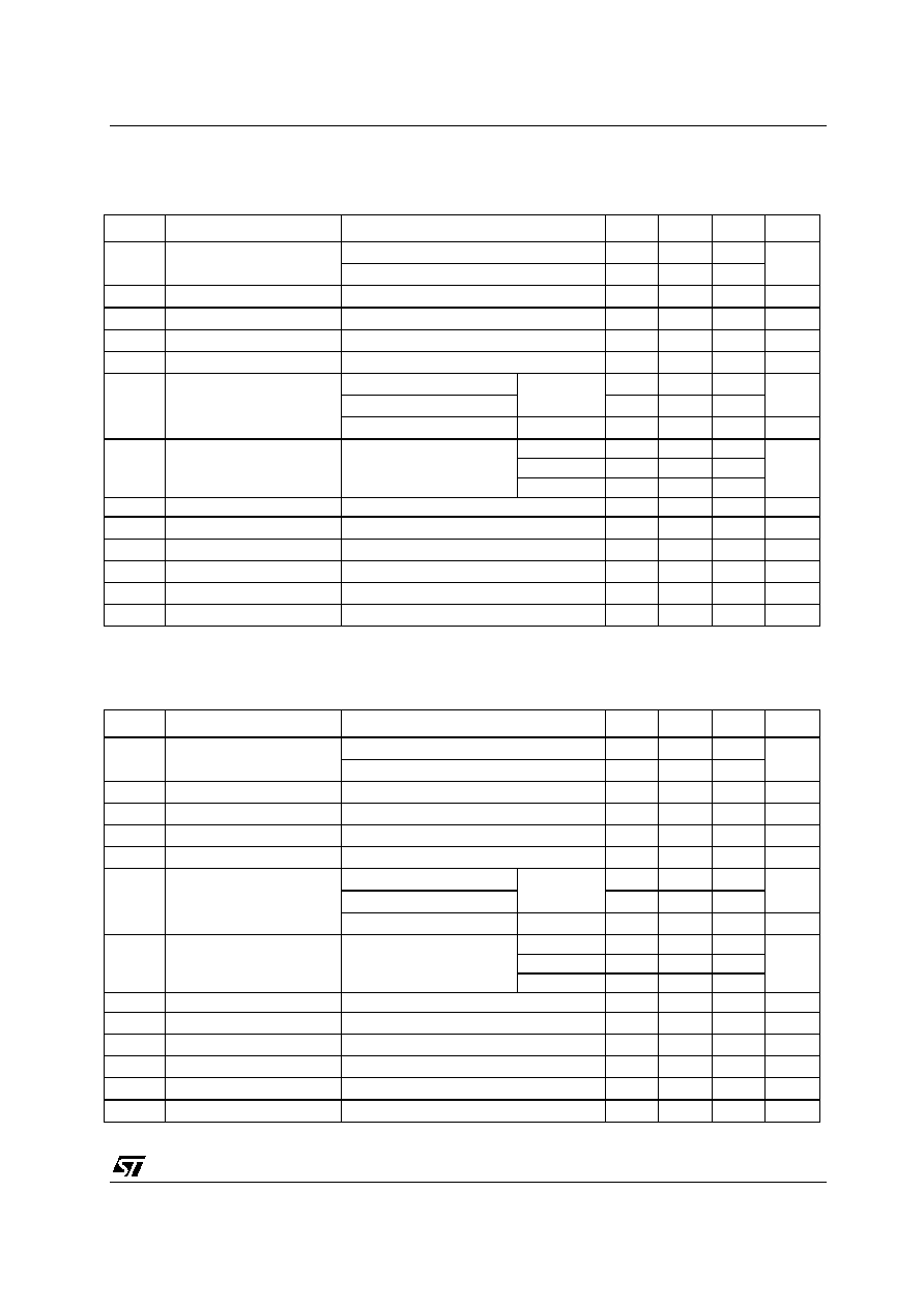
Figure 1: Test Circuits
Note: If the Inhibit pin is left floating, the regulator is in ON mode. However, to avoid any noise picking-up, it is suggested to ground it when
the Inhibit function is not used.
Figure 2: Pin Connection (top view)
Symbol
Parameter
Value
Unit
V
I
DC Input Voltage
20
V
I
O
Output Current
Internally Limited (*)
P
tot
Power Dissipation
Internally Limited (*)
T
stg
Storage Temperature Range
-40 to 150
∞C
T
op
Operating Junction Temperature Range
-40 to 125
∞C
Symbol
Parameter
SO-8
TO-92
Unit
R
thj-case
Thermal Resistance Junction-case
20
∞C/W
R
thj-amb
Thermal Resistance Junction-ambient
55
200
∞C/W
SO-8
TO-92
BOTTOM VIEW
PIN 1 = V
OUT
PIN 2 = GND
PIN 3 = V
IN

LE00AB/C SERIES
3/27
Table 3: Ordering Codes
(*) Available in Tape & Reel with the suffix "-TR".
(#) Available in Tape & Reel with the suffix "-TR" and in Ammopak with the suffix "-AP".
TYPE
SO-8 (*)
TO-92 (#)
OUTPUT VOLTAGE
LE12AB
LE12ABD
LE12ABZ
1.25 V
LE12C
LE12CD
LE12CZ
1.25 V
LE15AB
LE15ABD
LE15ABZ
1.5 V
LE15C
LE15CD
LE15CZ
1.5 V
LE25AB
LE25ABD
LE25ABZ
2.5 V
LE25C
LE25CD
LE25CZ
2.5 V
LE27AB
LE27ABD
LE27ABZ
2.7 V
LE27C
LE27CD
LE27CZ
2.7 V
LE30AB
LE30ABD
LE30ABZ
3 V
LE30C
LE30CD
LE30CZ
3 V
LE33AB
LE33ABD
LE33ABZ
3.3 V
LE33C
LE33CD
LE33CZ
3.3 V
LE35AB
LE35ABD
LE35ABZ
3.5 V
LE35C
LE35CD
LE35CZ
3.5 V
LE40AB
LE40ABD
LE40ABZ
4 V
LE40C
LE40CD
LE40CZ
4 V
LE45AB
LE45ABD
LE45ABZ
4.5 V
LE45C
LE45CD
LE45CZ
4.5 V
LE47AB
LE47ABD
LE47ABZ
4.7 V
LE47C
LE47CD
LE47CZ
4.7 V
LE50AB
LE50ABD
LE50ABZ
5 V
LE50C
LE50CD
LE50CZ
5 V
LE52AB
LE52ABD
LE52ABZ
5.2 V
LE52C
LE52CD
LE52CZ
5.2 V
LE55AB
LE55ABD
LE55ABZ
5.5 V
LE55C
LE55CD
LE55CZ
5.5 V
LE60AB
LE60ABD
LE60ABZ
6 V
LE60C
LE60CD
LE60CZ
6 V
LE80AB
LE80ABD
LE80ABZ
8 V
LE80C
LE80CD
LE80CZ
8 V
LE120AB
LE120ABD
LE120ABZ
12 V
LE120C
LE120CD
LE120CZ
12 V
LE00AB/C SERIES
4/27
Table 4: Electrical Characteristics For LE12AB (refer to the test circuits, T
j
= 25∞C, C
I
= 0.1 µF,
C
O
= 2.2
µ
F unless otherwise specified.)
Table 5: Electrical Characteristics For LE12C (refer to the test circuits, T
j
= 25∞C, C
I
= 0.1 µF,
C
O
= 2.2
µ
F unless otherwise specified.)
Symbol
Parameter
Test Conditions
Min.
Typ.
Max.
Unit
V
O
Output Voltage
I
O
= 10 mA, V
I
= 3.3 V
1.225
1.25
1.275
V
I
O
= 10 mA, V
I
= 3.3 V, T
a
= -25 to 85∞C
1.2
1.3
V
I
Operating Input Voltage
I
O
= 100 mA
2.5
18
V
I
O
Output Current Limit
150
mA
V
O
Line Regulation
V
I
= 2.5 to 18 V,
I
O
= 0.5 mA
3
15
mV
V
O
Load Regulation
V
I
= 2.8 V
I
O
= 0.5 to 100 mA
3
15
mV
I
d
Quiescent Current
V
I
= 2.5 to 18V, I
O
= 0mA
ON MODE
0.5
1
mA
V
I
= 2.5 to 18V, I
O
= 100mA
1.5
3
V
I
= 6 V
OFF MODE
50
100
µA
SVR
Supply Voltage Rejection
I
O
= 5 mA
V
I
= 3.5 ± 1 V
f = 120 Hz
82
dB
f = 1 KHz
77
f = 10 KHz
60
eN
Output Noise Voltage
B = 10 Hz to 100 KHz
50
µV
V
d
Dropout Voltage
I
O
= 100 mA
T
a
= -40 to 125∞C
1.25
V
V
IL
Control Input Logic Low
T
a
= -40 to 125∞C
0.8
V
V
IH
Control Input Logic High
T
a
= -40 to 125∞C
2
V
I
I
Control Input Current
V
I
= 6 V,
V
C
= 6 V
10
µA
C
O
Output Bypass Capacitance ESR = 0.1 to 10
I
O
= 0 to 100 mA
2
10
µF
Symbol
Parameter
Test Conditions
Min.
Typ.
Max.
Unit
V
O
Output Voltage
I
O
= 10 mA, V
I
= 3.3 V
1.225
1.25
1.275
V
I
O
= 10 mA, V
I
= 3.3 V, T
a
= -25 to 85∞C
1.2
1.3
V
I
Operating Input Voltage
I
O
= 100 mA
2.5
18
V
I
O
Output Current Limit
150
mA
V
O
Line Regulation
V
I
= 2.5 to 18 V,
I
O
= 0.5 mA
3
20
mV
V
O
Load Regulation
V
I
= 2.8 V
I
O
= 0.5 to 100 mA
3
25
mV
I
d
Quiescent Current
V
I
= 2.5 to 18V, I
O
= 0mA
ON MODE
0.5
1
mA
V
I
= 2.5 to 18V, I
O
= 100mA
1.5
3
V
I
= 6 V
OFF MODE
50
100
µA
SVR
Supply Voltage Rejection
I
O
= 5 mA
V
I
= 3.5 ± 1 V
f = 120 Hz
82
dB
f = 1 KHz
77
f = 10 KHz
60
eN
Output Noise Voltage
B = 10 Hz to 100 KHz
50
µV
V
d
Dropout Voltage
I
O
= 100 mA
T
a
= -40 to 125∞C
1.25
V
V
IL
Control Input Logic Low
T
a
= -40 to 125∞C
0.8
V
V
IH
Control Input Logic High
T
a
= -40 to 125∞C
2
V
I
I
Control Input Current
V
I
= 6 V,
V
C
= 6 V
10
µA
C
O
Output Bypass Capacitance ESR = 0.1 to 10
I
O
= 0 to 100 mA
2
10
µF
LE00AB/C SERIES
5/27
Table 6: Electrical Characteristics For LE15AB (refer to the test circuits, T
j
= 25∞C, C
I
= 0.1 µF,
C
O
= 2.2
µ
F unless otherwise specified.)
Table 7: Electrical Characteristics For LE15C (refer to the test circuits, T
j
= 25∞C, C
I
= 0.1 µF,
C
O
= 2.2
µ
F unless otherwise specified.)
Symbol
Parameter
Test Conditions
Min.
Typ.
Max.
Unit
V
O
Output Voltage
I
O
= 10 mA, V
I
= 3.5 V
1.47
1.5
1.53
V
I
O
= 10 mA, V
I
= 3.5 V, T
a
= -25 to 85∞C
1.44
1.56
V
I
Operating Input Voltage
I
O
= 100 mA
2.5
18
V
I
O
Output Current Limit
150
mA
V
O
Line Regulation
V
I
= 2.5 to 18 V,
I
O
= 0.5 mA
3
15
mV
V
O
Load Regulation
V
I
= 2.8 V
I
O
= 0.5 to 100 mA
3
15
mV
I
d
Quiescent Current
V
I
= 2.5 to 18V, I
O
= 0mA
ON MODE
0.5
1
mA
V
I
= 2.5 to 18V, I
O
= 100mA
1.5
3
V
I
= 6 V
OFF MODE
50
100
µA
SVR
Supply Voltage Rejection
I
O
= 5 mA
V
I
= 3.5 ± 1 V
f = 120 Hz
82
dB
f = 1 KHz
77
f = 10 KHz
60
eN
Output Noise Voltage
B = 10 Hz to 100 KHz
50
µV
V
d
Dropout Voltage
I
O
= 100 mA
T
a
= -40 to 125∞C
1
V
V
IL
Control Input Logic Low
T
a
= -40 to 125∞C
0.8
V
V
IH
Control Input Logic High
T
a
= -40 to 125∞C
2
V
I
I
Control Input Current
V
I
= 6 V,
V
C
= 6 V
10
µA
C
O
Output Bypass Capacitance ESR = 0.1 to 10
I
O
= 0 to 100 mA
2
10
µF
Symbol
Parameter
Test Conditions
Min.
Typ.
Max.
Unit
V
O
Output Voltage
I
O
= 10 mA, V
I
= 3.5 V
1.47
1.5
1.53
V
I
O
= 10 mA, V
I
= 3.5 V, T
a
= -25 to 85∞C
1.44
1.56
V
I
Operating Input Voltage
I
O
= 100 mA
2.5
18
V
I
O
Output Current Limit
150
mA
V
O
Line Regulation
V
I
= 2.5 to 18 V,
I
O
= 0.5 mA
3
20
mV
V
O
Load Regulation
V
I
= 2.8 V
I
O
= 0.5 to 100 mA
3
25
mV
I
d
Quiescent Current
V
I
= 2.5 to 18V, I
O
= 0mA
ON MODE
0.5
1
mA
V
I
= 2.5 to 18V, I
O
= 100mA
1.5
3
V
I
= 6 V
OFF MODE
50
100
µA
SVR
Supply Voltage Rejection
I
O
= 5 mA
V
I
= 3.5 ± 1 V
f = 120 Hz
82
dB
f = 1 KHz
77
f = 10 KHz
60
eN
Output Noise Voltage
B = 10 Hz to 100 KHz
50
µV
V
d
Dropout Voltage
I
O
= 100 mA
T
a
= -40 to 125∞C
1
V
V
IL
Control Input Logic Low
T
a
= -40 to 125∞C
0.8
V
V
IH
Control Input Logic High
T
a
= -40 to 125∞C
2
V
I
I
Control Input Current
V
I
= 6 V,
V
C
= 6 V
10
µA
C
O
Output Bypass Capacitance ESR = 0.1 to 10
I
O
= 0 to 100 mA
2
10
µF

LE00AB/C SERIES
6/27
Table 8: Electrical Characteristics For LE25AB (refer to the test circuits, T
j
= 25∞C, C
I
= 0.1 µF,
C
O
= 2.2
µ
F unless otherwise specified.)
Table 9: Electrical Characteristics For LE25C (refer to the test circuits, T
j
= 25∞C, C
I
= 0.1 µF,
C
O
= 2.2
µ
F unless otherwise specified.)
Symbol
Parameter
Test Conditions
Min.
Typ.
Max.
Unit
V
O
Output Voltage
I
O
= 10 mA, V
I
= 4.5 V
2.475
2.5
2.525
V
I
O
= 10 mA, V
I
= 4.5 V, T
a
= -25 to 85∞C
2.45
2.55
V
I
Operating Input Voltage
I
O
= 100 mA
18
V
I
O
Output Current Limit
150
mA
V
O
Line Regulation
V
I
= 3.2 to 18 V,
I
O
= 0.5 mA
3
15
mV
V
O
Load Regulation
V
I
= 3.5 V
I
O
= 0.5 to 100 mA
3
15
mV
I
d
Quiescent Current
V
I
= 3.5 to 18V, I
O
= 0mA
ON MODE
0.5
1
mA
V
I
= 3.5 to 18V, I
O
= 100mA
1.5
3
V
I
= 6 V
OFF MODE
50
100
µA
SVR
Supply Voltage Rejection
I
O
= 5 mA
V
I
= 4.5 ± 1 V
f = 120 Hz
82
dB
f = 1 KHz
77
f = 10 KHz
60
eN
Output Noise Voltage
B = 10 Hz to 100 KHz
50
µV
V
d
Dropout Voltage
I
O
= 100 mA
0.2
0.4
V
I
O
= 100 mA
T
a
= -40 to 125∞C
0.5
V
IL
Control Input Logic Low
T
a
= -40 to 125∞C
0.8
V
V
IH
Control Input Logic High
T
a
= -40 to 125∞C
2
V
I
I
Control Input Current
V
I
= 6 V,
V
C
= 6 V
10
µA
C
O
Output Bypass Capacitance ESR = 0.1 to 10
I
O
= 0 to 100 mA
2
10
µF
Symbol
Parameter
Test Conditions
Min.
Typ.
Max.
Unit
V
O
Output Voltage
I
O
= 10 mA, V
I
= 4.5 V
2.45
2.5
2.55
V
I
O
= 10 mA, V
I
= 4.5 V, T
a
= -25 to 85∞C
2.4
2.6
V
I
Operating Input Voltage
I
O
= 100 mA
18
V
I
O
Output Current Limit
150
mA
V
O
Line Regulation
V
I
= 3.2 to 18 V,
I
O
= 0.5 mA
3
20
mV
V
O
Load Regulation
V
I
= 3.5 V
I
O
= 0.5 to 100 mA
3
25
mV
I
d
Quiescent Current
V
I
= 3.5 to 18V, I
O
= 0mA
ON MODE
0.5
1
mA
V
I
= 3.5 to 18V, I
O
= 100mA
1.5
3
V
I
= 6 V
OFF MODE
50
100
µA
SVR
Supply Voltage Rejection
I
O
= 5 mA
V
I
= 4.5 ± 1 V
f = 120 Hz
82
dB
f = 1 KHz
77
f = 10 KHz
60
eN
Output Noise Voltage
B = 10 Hz to 100 KHz
50
µV
V
d
Dropout Voltage
I
O
= 100 mA
0.2
0.4
V
I
O
= 100 mA
T
a
= -40 to 125∞C
0.5
V
IL
Control Input Logic Low
T
a
= -40 to 125∞C
0.8
V
V
IH
Control Input Logic High
T
a
= -40 to 125∞C
2
V
I
I
Control Input Current
V
I
= 6 V,
V
C
= 6 V
10
µA
C
O
Output Bypass Capacitance ESR = 0.1 to 10
I
O
= 0 to 100 mA
2
10
µF

LE00AB/C SERIES
7/27
Table 10: Electrical Characteristics For LE27AB (refer to the test circuits, T
j
= 25∞C, C
I
= 0.1 µF,
C
O
= 2.2
µ
F unless otherwise specified.)
Table 11: Electrical Characteristics For LE27C (refer to the test circuits, T
j
= 25∞C, C
I
= 0.1 µF,
C
O
= 2.2
µ
F unless otherwise specified.)
Symbol
Parameter
Test Conditions
Min.
Typ.
Max.
Unit
V
O
Output Voltage
I
O
= 10 mA, V
I
= 4.7 V
2.673
2.7
2.727
V
I
O
= 10 mA, V
I
= 4.7 V, T
a
= -25 to 85∞C
2.646
2.754
V
I
Operating Input Voltage
I
O
= 100 mA
18
V
I
O
Output Current Limit
150
mA
V
O
Line Regulation
V
I
= 3.4 to 18 V,
I
O
= 0.5 mA
3
15
mV
V
O
Load Regulation
V
I
= 3.7 V
I
O
= 0.5 to 100 mA
3
15
mV
I
d
Quiescent Current
V
I
= 3.7 to 18V, I
O
= 0mA
ON MODE
0.5
1
mA
V
I
= 3.7 to 18V, I
O
= 100mA
1.5
3
V
I
= 6 V
OFF MODE
50
100
µA
SVR
Supply Voltage Rejection
I
O
= 5 mA
V
I
= 4.7 ± 1 V
f = 120 Hz
82
dB
f = 1 KHz
77
f = 10 KHz
60
eN
Output Noise Voltage
B = 10 Hz to 100 KHz
50
µV
V
d
Dropout Voltage
I
O
= 100 mA
0.2
0.4
V
I
O
= 100 mA
T
a
= -40 to 125∞C
0.5
V
IL
Control Input Logic Low
T
a
= -40 to 125∞C
0.8
V
V
IH
Control Input Logic High
T
a
= -40 to 125∞C
2
V
I
I
Control Input Current
V
I
= 6 V,
V
C
= 6 V
10
µA
C
O
Output Bypass Capacitance ESR = 0.1 to 10
I
O
= 0 to 100 mA
2
10
µF
Symbol
Parameter
Test Conditions
Min.
Typ.
Max.
Unit
V
O
Output Voltage
I
O
= 10 mA, V
I
= 4.7 V
2.646
2.7
2.754
V
I
O
= 10 mA, V
I
= 4.7 V, T
a
= -25 to 85∞C
2.592
2.808
V
I
Operating Input Voltage
I
O
= 100 mA
18
V
I
O
Output Current Limit
150
mA
V
O
Line Regulation
V
I
= 3.4 to 18 V,
I
O
= 0.5 mA
3
20
mV
V
O
Load Regulation
V
I
= 3.7 V
I
O
= 0.5 to 100 mA
3
25
mV
I
d
Quiescent Current
V
I
= 3.7 to 18V, I
O
= 0mA
ON MODE
0.5
1
mA
V
I
= 3.7 to 18V, I
O
= 100mA
1.5
3
V
I
= 6 V
OFF MODE
50
100
µA
SVR
Supply Voltage Rejection
I
O
= 5 mA
V
I
= 4.7 ± 1 V
f = 120 Hz
82
dB
f = 1 KHz
77
f = 10 KHz
60
eN
Output Noise Voltage
B = 10 Hz to 100 KHz
50
µV
V
d
Dropout Voltage
I
O
= 100 mA
0.2
0.4
V
I
O
= 100 mA
T
a
= -40 to 125∞C
0.5
V
IL
Control Input Logic Low
T
a
= -40 to 125∞C
0.8
V
V
IH
Control Input Logic High
T
a
= -40 to 125∞C
2
V
I
I
Control Input Current
V
I
= 6 V,
V
C
= 6 V
10
µA
C
O
Output Bypass Capacitance ESR = 0.1 to 10
I
O
= 0 to 100 mA
2
10
µF
LE00AB/C SERIES
8/27
Table 12: Electrical Characteristics For LE30AB (refer to the test circuits, T
j
= 25∞C, C
I
= 0.1 µF,
C
O
= 2.2
µ
F unless otherwise specified.)
Table 13: Electrical Characteristics For LE30C (refer to the test circuits, T
j
= 25∞C, C
I
= 0.1 µF,
C
O
= 2.2
µ
F unless otherwise specified.)
Symbol
Parameter
Test Conditions
Min.
Typ.
Max.
Unit
V
O
Output Voltage
I
O
= 10 mA, V
I
= 5 V
2.970
3
3.030
V
I
O
= 10 mA, V
I
= 5 V, T
a
= -25 to 85∞C
2.940
3.060
V
I
Operating Input Voltage
I
O
= 100 mA
18
V
I
O
Output Current Limit
150
mA
V
O
Line Regulation
V
I
= 3.7 to 18 V,
I
O
= 0.5 mA
3
15
mV
V
O
Load Regulation
V
I
= 4 V
I
O
= 0.5 to 100 mA
3
15
mV
I
d
Quiescent Current
V
I
= 4 to 18V, I
O
= 0mA
ON MODE
0.5
1
mA
V
I
= 4 to 18V, I
O
= 100mA
1.5
3
V
I
= 6 V
OFF MODE
50
100
µA
SVR
Supply Voltage Rejection
I
O
= 5 mA
V
I
= 5 ± 1 V
f = 120 Hz
81
dB
f = 1 KHz
76
f = 10 KHz
60
eN
Output Noise Voltage
B = 10 Hz to 100 KHz
50
µV
V
d
Dropout Voltage
I
O
= 100 mA
0.2
0.4
V
I
O
= 100 mA
T
a
= -40 to 125∞C
0.5
V
IL
Control Input Logic Low
T
a
= -40 to 125∞C
0.8
V
V
IH
Control Input Logic High
T
a
= -40 to 125∞C
2
V
I
I
Control Input Current
V
I
= 6 V,
V
C
= 6 V
10
µA
C
O
Output Bypass Capacitance ESR = 0.1 to 10
I
O
= 0 to 100 mA
2
10
µF
Symbol
Parameter
Test Conditions
Min.
Typ.
Max.
Unit
V
O
Output Voltage
I
O
= 10 mA, V
I
= 5 V
2.940
3
3.060
I
O
= 10 mA, V
I
= 5 V, T
a
= -25 to 85∞C
2.880
3.120
V
I
Operating Input Voltage
I
O
= 100 mA
18
V
I
O
Output Current Limit
150
mA
V
O
Line Regulation
V
I
= 3.7 to 18 V,
I
O
= 0.5 mA
3
20
mV
V
O
Load Regulation
V
I
= 4 V
I
O
= 0.5 to 100 mA
3
25
mV
I
d
Quiescent Current
V
I
= 4 to 18V, I
O
= 0mA
ON MODE
0.5
1
mA
V
I
= 4 to 18V, I
O
= 100mA
1.5
3
V
I
= 6 V
OFF MODE
50
100
µA
SVR
Supply Voltage Rejection
I
O
= 5 mA
V
I
= 5 ± 1 V
f = 120 Hz
81
dB
f = 1 KHz
76
f = 10 KHz
60
eN
Output Noise Voltage
B = 10 Hz to 100 KHz
50
µV
V
d
Dropout Voltage
I
O
= 100 mA
0.2
0.4
V
I
O
= 100 mA
T
a
= -40 to 125∞C
0.5
V
IL
Control Input Logic Low
T
a
= -40 to 125∞C
0.8
V
V
IH
Control Input Logic High
T
a
= -40 to 125∞C
2
V
I
I
Control Input Current
V
I
= 6 V,
V
C
= 6 V
10
µA
C
O
Output Bypass Capacitance ESR = 0.1 to 10
I
O
= 0 to 100 mA
2
10
µF

LE00AB/C SERIES
9/27
Table 14: Electrical Characteristics For LE33AB (refer to the test circuits, T
j
= 25∞C, C
I
= 0.1 µF,
C
O
= 2.2
µ
F unless otherwise specified.)
Table 15: Electrical Characteristics For LE33C (refer to the test circuits, T
j
= 25∞C, C
I
= 0.1 µF,
C
O
= 2.2
µ
F unless otherwise specified.)
Symbol
Parameter
Test Conditions
Min.
Typ.
Max.
Unit
V
O
Output Voltage
I
O
= 10 mA, V
I
= 5.3 V
3.267
3.3
3.333
V
I
O
= 10 mA, V
I
= 5.3 V, T
a
= -25 to 85∞C
3.234
3.366
V
I
Operating Input Voltage
I
O
= 100 mA
18
V
I
O
Output Current Limit
150
mA
V
O
Line Regulation
V
I
= 4 to 18 V,
I
O
= 0.5 mA
3
15
mV
V
O
Load Regulation
V
I
= 4.3 V
I
O
= 0.5 to 100 mA
3
15
mV
I
d
Quiescent Current
V
I
= 4.3 to 18V, I
O
= 0mA
ON MODE
0.5
1
mA
V
I
= 4.3 to 18V, I
O
= 100mA
1.5
3
V
I
= 6 V
OFF MODE
50
100
µA
SVR
Supply Voltage Rejection
I
O
= 5 mA
V
I
= 5.3 ± 1 V
f = 120 Hz
80
dB
f = 1 KHz
75
f = 10 KHz
60
eN
Output Noise Voltage
B = 10 Hz to 100 KHz
50
µV
V
d
Dropout Voltage
I
O
= 100 mA
0.2
0.4
V
I
O
= 100 mA
T
a
= -40 to 125∞C
0.5
V
IL
Control Input Logic Low
T
a
= -40 to 125∞C
0.8
V
V
IH
Control Input Logic High
T
a
= -40 to 125∞C
2
V
I
I
Control Input Current
V
I
= 6 V,
V
C
= 6 V
10
µA
C
O
Output Bypass Capacitance ESR = 0.1 to 10
I
O
= 0 to 100 mA
2
10
µF
Symbol
Parameter
Test Conditions
Min.
Typ.
Max.
Unit
V
O
Output Voltage
I
O
= 10 mA, V
I
= 5.3 V
3.234
3.3
3.366
V
I
O
= 10 mA, V
I
= 5.3 V, T
a
= -25 to 85∞C
3.168
3.432
V
I
Operating Input Voltage
I
O
= 100 mA
18
V
I
O
Output Current Limit
150
mA
V
O
Line Regulation
V
I
= 4 to 18 V,
I
O
= 0.5 mA
3
20
mV
V
O
Load Regulation
V
I
= 4.3 V
I
O
= 0.5 to 100 mA
3
25
mV
I
d
Quiescent Current
V
I
= 4.3 to 18V, I
O
= 0mA
ON MODE
0.5
1
mA
V
I
= 4.3 to 18V, I
O
= 100mA
1.5
3
V
I
= 6 V
OFF MODE
50
100
µA
SVR
Supply Voltage Rejection
I
O
= 5 mA
V
I
= 5.3 ± 1 V
f = 120 Hz
80
dB
f = 1 KHz
75
f = 10 KHz
60
eN
Output Noise Voltage
B = 10 Hz to 100 KHz
50
µV
V
d
Dropout Voltage
I
O
= 100 mA
0.2
0.4
V
I
O
= 100 mA
T
a
= -40 to 125∞C
0.5
V
IL
Control Input Logic Low
T
a
= -40 to 125∞C
0.8
V
V
IH
Control Input Logic High
T
a
= -40 to 125∞C
2
V
I
I
Control Input Current
V
I
= 6 V,
V
C
= 6 V
10
µA
C
O
Output Bypass Capacitance ESR = 0.1 to 10
I
O
= 0 to 100 mA
2
10
µF

LE00AB/C SERIES
10/27
Table 16: Electrical Characteristics For LE35AB (refer to the test circuits, T
j
= 25∞C, C
I
= 0.1 µF,
C
O
= 2.2
µ
F unless otherwise specified.)
Table 17: Electrical Characteristics For LE35C (refer to the test circuits, T
j
= 25∞C, C
I
= 0.1 µF,
C
O
= 2.2
µ
F unless otherwise specified.)
Symbol
Parameter
Test Conditions
Min.
Typ.
Max.
Unit
V
O
Output Voltage
I
O
= 10 mA, V
I
= 5.5 V
3.465
3.5
3.535
V
I
O
= 10 mA, V
I
= 5.5 V, T
a
= -25 to 85∞C
3.43
3.57
V
I
Operating Input Voltage
I
O
= 100 mA
18
V
I
O
Output Current Limit
150
mA
V
O
Line Regulation
V
I
= 4.2 to 18 V,
I
O
= 0.5 mA
3
15
mV
V
O
Load Regulation
V
I
= 4.5 V
I
O
= 0.5 to 100 mA
3
15
mV
I
d
Quiescent Current
V
I
= 4.5 to 18V, I
O
= 0mA
ON MODE
0.5
1
mA
V
I
= 4.5 to 18V, I
O
= 100mA
1.5
3
V
I
= 6 V
OFF MODE
50
100
µA
SVR
Supply Voltage Rejection
I
O
= 5 mA
V
I
= 5.5 ± 1 V
f = 120 Hz
79
dB
f = 1 KHz
74
f = 10 KHz
60
eN
Output Noise Voltage
B = 10 Hz to 100 KHz
50
µV
V
d
Dropout Voltage
I
O
= 100 mA
0.2
0.4
V
I
O
= 100 mA
T
a
= -40 to 125∞C
0.5
V
IL
Control Input Logic Low
T
a
= -40 to 125∞C
0.8
V
V
IH
Control Input Logic High
T
a
= -40 to 125∞C
2
V
I
I
Control Input Current
V
I
= 6 V,
V
C
= 6 V
10
µA
C
O
Output Bypass Capacitance ESR = 0.1 to 10
I
O
= 0 to 100 mA
2
10
µF
Symbol
Parameter
Test Conditions
Min.
Typ.
Max.
Unit
V
O
Output Voltage
I
O
= 10 mA, V
I
= 5.5 V
3.43
3.5
3.57
V
I
O
= 10 mA, V
I
= 5.5 V, T
a
= -25 to 85∞C
3.36
3.64
V
I
Operating Input Voltage
I
O
= 100 mA
18
V
I
O
Output Current Limit
150
mA
V
O
Line Regulation
V
I
= 4.2 to 18 V,
I
O
= 0.5 mA
3
20
mV
V
O
Load Regulation
V
I
= 4.5 V
I
O
= 0.5 to 100 mA
3
25
mV
I
d
Quiescent Current
V
I
= 4.5 to 18V, I
O
= 0mA
ON MODE
0.5
1
mA
V
I
= 4.5 to 18V, I
O
= 100mA
1.5
3
V
I
= 6 V
OFF MODE
50
100
µA
SVR
Supply Voltage Rejection
I
O
= 5 mA
V
I
= 5.5 ± 1 V
f = 120 Hz
79
dB
f = 1 KHz
74
f = 10 KHz
60
eN
Output Noise Voltage
B = 10 Hz to 100 KHz
50
µV
V
d
Dropout Voltage
I
O
= 100 mA
0.2
0.4
V
I
O
= 100 mA
T
a
= -40 to 125∞C
0.5
V
IL
Control Input Logic Low
T
a
= -40 to 125∞C
0.8
V
V
IH
Control Input Logic High
T
a
= -40 to 125∞C
2
V
I
I
Control Input Current
V
I
= 6 V,
V
C
= 6 V
10
µA
C
O
Output Bypass Capacitance ESR = 0.1 to 10
I
O
= 0 to 100 mA
2
10
µF

LE00AB/C SERIES
11/27
Table 18: Electrical Characteristics For LE40AB (refer to the test circuits, T
j
= 25∞C, C
I
= 0.1 µF,
C
O
= 2.2
µ
F unless otherwise specified.)
Table 19: Electrical Characteristics For LE40C (refer to the test circuits, T
j
= 25∞C, C
I
= 0.1 µF,
C
O
= 2.2
µ
F unless otherwise specified.)
Symbol
Parameter
Test Conditions
Min.
Typ.
Max.
Unit
V
O
Output Voltage
I
O
= 10 mA, V
I
= 6 V
3.96
4
4.04
V
I
O
= 10 mA, V
I
= 6 V, T
a
= -25 to 85∞C
3.92
4.08
V
I
Operating Input Voltage
I
O
= 100 mA
18
V
I
O
Output Current Limit
150
mA
V
O
Line Regulation
V
I
= 4.7 to 18 V,
I
O
= 0.5 mA
4
20
mV
V
O
Load Regulation
V
I
= 5 V
I
O
= 0.5 to 100 mA
3
15
mV
I
d
Quiescent Current
V
I
= 5 to 18V, I
O
= 0mA
ON MODE
0.5
1
mA
V
I
= 5 to 18V, I
O
= 100mA
1.5
3
V
I
= 6 V
OFF MODE
50
100
µA
SVR
Supply Voltage Rejection
I
O
= 5 mA
V
I
= 6 ± 1 V
f = 120 Hz
78
dB
f = 1 KHz
73
f = 10 KHz
60
eN
Output Noise Voltage
B = 10 Hz to 100 KHz
50
µV
V
d
Dropout Voltage
I
O
= 100 mA
0.2
0.4
V
I
O
= 100 mA
T
a
= -40 to 125∞C
0.5
V
IL
Control Input Logic Low
T
a
= -40 to 125∞C
0.8
V
V
IH
Control Input Logic High
T
a
= -40 to 125∞C
2
V
I
I
Control Input Current
V
I
= 6 V,
V
C
= 6 V
10
µA
C
O
Output Bypass Capacitance ESR = 0.1 to 10
I
O
= 0 to 100 mA
2
10
µF
Symbol
Parameter
Test Conditions
Min.
Typ.
Max.
Unit
V
O
Output Voltage
I
O
= 10 mA, V
I
= 6 V
3.92
4
4.08
V
I
O
= 10 mA, V
I
= 6 V, T
a
= -25 to 85∞C
3.84
4.16
V
I
Operating Input Voltage
I
O
= 100 mA
18
V
I
O
Output Current Limit
150
mA
V
O
Line Regulation
V
I
= 4.7 to 18 V,
I
O
= 0.5 mA
4
30
mV
V
O
Load Regulation
V
I
= 5 V
I
O
= 0.5 to 100 mA
3
25
mV
I
d
Quiescent Current
V
I
= 5 to 18V, I
O
= 0mA
ON MODE
0.5
1
mA
V
I
= 5 to 18V, I
O
= 100mA
1.5
3
V
I
= 6 V
OFF MODE
50
100
µA
SVR
Supply Voltage Rejection
I
O
= 5 mA
V
I
= 6 ± 1 V
f = 120 Hz
78
dB
f = 1 KHz
73
f = 10 KHz
60
eN
Output Noise Voltage
B = 10 Hz to 100 KHz
50
µV
V
d
Dropout Voltage
I
O
= 100 mA
0.2
0.4
V
I
O
= 100 mA
T
a
= -40 to 125∞C
0.5
V
IL
Control Input Logic Low
T
a
= -40 to 125∞C
0.8
V
V
IH
Control Input Logic High
T
a
= -40 to 125∞C
2
V
I
I
Control Input Current
V
I
= 6 V,
V
C
= 6 V
10
µA
C
O
Output Bypass Capacitance ESR = 0.1 to 10
I
O
= 0 to 100 mA
2
10
µF

LE00AB/C SERIES
12/27
Table 20: Electrical Characteristics For LE45AB (refer to the test circuits, T
j
= 25∞C, C
I
= 0.1 µF,
C
O
= 2.2
µ
F unless otherwise specified.)
Table 21: Electrical Characteristics For LE45C (refer to the test circuits, T
j
= 25∞C, C
I
= 0.1 µF,
C
O
= 2.2
µ
F unless otherwise specified.)
Symbol
Parameter
Test Conditions
Min.
Typ.
Max.
Unit
V
O
Output Voltage
I
O
= 10 mA, V
I
= 6.5 V
4.445
4.5
4.545
V
I
O
= 10 mA, V
I
= 6.5 V, T
a
= -25 to 85∞C
4.41
4.59
V
I
Operating Input Voltage
I
O
= 100 mA
18
V
I
O
Output Current Limit
150
mA
V
O
Line Regulation
V
I
= 5.2 to 18 V,
I
O
= 0.5 mA
4
20
mV
V
O
Load Regulation
V
I
= 5.5 V
I
O
= 0.5 to 100 mA
3
15
mV
I
d
Quiescent Current
V
I
= 5.5 to 18V, I
O
= 0mA
ON MODE
0.5
1
mA
V
I
= 5.5 to 18V, I
O
= 100mA
1.5
3
V
I
= 6 V
OFF MODE
50
100
µA
SVR
Supply Voltage Rejection
I
O
= 5 mA
V
I
= 6.5 ± 1 V
f = 120 Hz
77
dB
f = 1 KHz
72
f = 10 KHz
60
eN
Output Noise Voltage
B = 10 Hz to 100 KHz
50
µV
V
d
Dropout Voltage
I
O
= 100 mA
0.2
0.4
V
I
O
= 100 mA
T
a
= -40 to 125∞C
0.5
V
IL
Control Input Logic Low
T
a
= -40 to 125∞C
0.8
V
V
IH
Control Input Logic High
T
a
= -40 to 125∞C
2
V
I
I
Control Input Current
V
I
= 6 V,
V
C
= 6 V
10
µA
C
O
Output Bypass Capacitance ESR = 0.1 to 10
I
O
= 0 to 100 mA
2
10
µF
Symbol
Parameter
Test Conditions
Min.
Typ.
Max.
Unit
V
O
Output Voltage
I
O
= 10 mA, V
I
= 6.5 V
4.41
4.5
4.59
V
I
O
= 10 mA, V
I
= 6.5 V, T
a
= -25 to 85∞C
4.32
4.68
V
I
Operating Input Voltage
I
O
= 100 mA
18
V
I
O
Output Current Limit
150
mA
V
O
Line Regulation
V
I
= 5.2 to 18 V,
I
O
= 0.5 mA
4
30
mV
V
O
Load Regulation
V
I
= 5.5 V
I
O
= 0.5 to 100 mA
3
25
mV
I
d
Quiescent Current
V
I
= 5.5 to 18V, I
O
= 0mA
ON MODE
0.5
1
mA
V
I
= 5.5 to 18V, I
O
= 100mA
1.5
3
V
I
= 6 V
OFF MODE
50
100
µA
SVR
Supply Voltage Rejection
I
O
= 5 mA
V
I
= 6.5 ± 1 V
f = 120 Hz
77
dB
f = 1 KHz
72
f = 10 KHz
60
eN
Output Noise Voltage
B = 10 Hz to 100 KHz
50
µV
V
d
Dropout Voltage
I
O
= 100 mA
0.2
0.4
V
I
O
= 100 mA
T
a
= -40 to 125∞C
0.5
V
IL
Control Input Logic Low
T
a
= -40 to 125∞C
0.8
V
V
IH
Control Input Logic High
T
a
= -40 to 125∞C
2
V
I
I
Control Input Current
V
I
= 6 V,
V
C
= 6 V
10
µA
C
O
Output Bypass Capacitance ESR = 0.1 to 10
I
O
= 0 to 100 mA
2
10
µF

LE00AB/C SERIES
13/27
Table 22: Electrical Characteristics For LE47AB (refer to the test circuits, T
j
= 25∞C, C
I
= 0.1 µF,
C
O
= 2.2
µ
F unless otherwise specified.)
Table 23: Electrical Characteristics For LE47C (refer to the test circuits, T
j
= 25∞C, C
I
= 0.1 µF,
C
O
= 2.2
µ
F unless otherwise specified.)
Symbol
Parameter
Test Conditions
Min.
Typ.
Max.
Unit
V
O
Output Voltage
I
O
= 10 mA, V
I
= 6.7 V
4.653
4.7
4.747
V
I
O
= 10 mA, V
I
= 6.7 V, T
a
= -25 to 85∞C
4.606
4.794
V
I
Operating Input Voltage
I
O
= 100 mA
18
V
I
O
Output Current Limit
150
mA
V
O
Line Regulation
V
I
= 5.4 to 18 V,
I
O
= 0.5 mA
4
20
mV
V
O
Load Regulation
V
I
= 5.7 V
I
O
= 0.5 to 100 mA
3
15
mV
I
d
Quiescent Current
V
I
= 5.7 to 18V, I
O
= 0mA
ON MODE
0.5
1
mA
V
I
= 5.7 to 18V, I
O
= 100mA
1.5
3
V
I
= 6 V
OFF MODE
50
100
µA
SVR
Supply Voltage Rejection
I
O
= 5 mA
V
I
= 6.7 ± 1 V
f = 120 Hz
77
dB
f = 1 KHz
72
f = 10 KHz
60
eN
Output Noise Voltage
B = 10 Hz to 100 KHz
50
µV
V
d
Dropout Voltage
I
O
= 100 mA
0.2
0.4
V
I
O
= 100 mA
T
a
= -40 to 125∞C
0.5
V
IL
Control Input Logic Low
T
a
= -40 to 125∞C
0.8
V
V
IH
Control Input Logic High
T
a
= -40 to 125∞C
2
V
I
I
Control Input Current
V
I
= 6 V,
V
C
= 6 V
10
µA
C
O
Output Bypass Capacitance ESR = 0.1 to 10
I
O
= 0 to 100 mA
2
10
µF
Symbol
Parameter
Test Conditions
Min.
Typ.
Max.
Unit
V
O
Output Voltage
I
O
= 10 mA, V
I
= 6.7 V
4.606
4.7
4.794
V
I
O
= 10 mA, V
I
= 6.7 V, T
a
= -25 to 85∞C
4.512
4.888
V
I
Operating Input Voltage
I
O
= 100 mA
18
V
I
O
Output Current Limit
150
mA
V
O
Line Regulation
V
I
= 5.4 to 18 V,
I
O
= 0.5 mA
4
30
mV
V
O
Load Regulation
V
I
= 5.7 V
I
O
= 0.5 to 100 mA
3
25
mV
I
d
Quiescent Current
V
I
= 5.7 to 18V, I
O
= 0mA
ON MODE
0.5
1
mA
V
I
= 5.7 to 18V, I
O
= 100mA
1.5
3
V
I
= 6 V
OFF MODE
50
100
µA
SVR
Supply Voltage Rejection
I
O
= 5 mA
V
I
= 6.7 ± 1 V
f = 120 Hz
77
dB
f = 1 KHz
72
f = 10 KHz
60
eN
Output Noise Voltage
B = 10 Hz to 100 KHz
50
µV
V
d
Dropout Voltage
I
O
= 100 mA
0.2
0.4
V
I
O
= 100 mA
T
a
= -40 to 125∞C
0.5
V
IL
Control Input Logic Low
T
a
= -40 to 125∞C
0.8
V
V
IH
Control Input Logic High
T
a
= -40 to 125∞C
2
V
I
I
Control Input Current
V
I
= 6 V,
V
C
= 6 V
10
µA
C
O
Output Bypass Capacitance ESR = 0.1 to 10
I
O
= 0 to 100 mA
2
10
µF

LE00AB/C SERIES
14/27
Table 24: Electrical Characteristics For LE50AB (refer to the test circuits, T
j
= 25∞C, C
I
= 0.1 µF,
C
O
= 2.2
µ
F unless otherwise specified.)
Table 25: Electrical Characteristics For LE50C (refer to the test circuits, T
j
= 25∞C, C
I
= 0.1 µF,
C
O
= 2.2
µ
F unless otherwise specified.)
Symbol
Parameter
Test Conditions
Min.
Typ.
Max.
Unit
V
O
Output Voltage
I
O
= 10 mA, V
I
= 7 V
4.95
5
5.05
V
I
O
= 10 mA, V
I
= 7 V, T
a
= -25 to 85∞C
4.9
5.1
V
I
Operating Input Voltage
I
O
= 100 mA
18
V
I
O
Output Current Limit
150
350
425
mA
V
O
Line Regulation
V
I
= 5.7 to 18 V,
I
O
= 0.5 mA
4
20
mV
V
O
Load Regulation
V
I
= 6 V
I
O
= 0.5 to 100 mA
3
15
mV
I
d
Quiescent Current
V
I
= 6 to 18V, I
O
= 0mA
ON MODE
0.5
1
mA
V
I
= 6 to 18V, I
O
= 100mA
1.5
3
V
I
= 6 V
OFF MODE
50
100
µA
SVR
Supply Voltage Rejection
I
O
= 5 mA
V
I
= 7 ± 1 V
f = 120 Hz
76
dB
f = 1 KHz
71
f = 10 KHz
60
eN
Output Noise Voltage
B = 10 Hz to 100 KHz
50
µV
V
d
Dropout Voltage
I
O
= 100 mA
0.2
0.4
V
I
O
= 100 mA
T
a
= -40 to 125∞C
0.5
V
IL
Control Input Logic Low
T
a
= -40 to 125∞C
0.8
V
V
IH
Control Input Logic High
T
a
= -40 to 125∞C
2
V
I
I
Control Input Current
V
I
= 6 V,
V
C
= 6 V
10
µA
C
O
Output Bypass Capacitance ESR = 0.1 to 10
I
O
= 0 to 100 mA
2
10
µF
Symbol
Parameter
Test Conditions
Min.
Typ.
Max.
Unit
V
O
Output Voltage
I
O
= 10 mA, V
I
= 7 V
4.9
5
5.1
V
I
O
= 10 mA, V
I
= 7 V, T
a
= -25 to 85∞C
4.8
5.2
V
I
Operating Input Voltage
I
O
= 100 mA
18
V
I
O
Output Current Limit
150
350
425
mA
V
O
Line Regulation
V
I
= 5.7 to 18 V,
I
O
= 0.5 mA
4
30
mV
V
O
Load Regulation
V
I
= 6 V
I
O
= 0.5 to 100 mA
3
25
mV
I
d
Quiescent Current
V
I
= 6 to 18V, I
O
= 0mA
ON MODE
0.5
1
mA
V
I
= 6 to 18V, I
O
= 100mA
1.5
3
V
I
= 6 V
OFF MODE
50
100
µA
SVR
Supply Voltage Rejection
I
O
= 5 mA
V
I
= 7 ± 1 V
f = 120 Hz
76
dB
f = 1 KHz
71
f = 10 KHz
60
eN
Output Noise Voltage
B = 10 Hz to 100 KHz
50
µV
V
d
Dropout Voltage
I
O
= 100 mA
0.2
0.4
V
I
O
= 100 mA
T
a
= -40 to 125∞C
0.5
V
IL
Control Input Logic Low
T
a
= -40 to 125∞C
0.8
V
V
IH
Control Input Logic High
T
a
= -40 to 125∞C
2
V
I
I
Control Input Current
V
I
= 6 V,
V
C
= 6 V
10
µA
C
O
Output Bypass Capacitance ESR = 0.1 to 10
I
O
= 0 to 100 mA
2
10
µF

LE00AB/C SERIES
15/27
Table 26: Electrical Characteristics For LE52AB (refer to the test circuits, T
j
= 25∞C, C
I
= 0.1 µF,
C
O
= 2.2
µ
F unless otherwise specified.)
Table 27: Electrical Characteristics For LE52C (refer to the test circuits, T
j
= 25∞C, C
I
= 0.1 µF,
C
O
= 2.2
µ
F unless otherwise specified.)
Symbol
Parameter
Test Conditions
Min.
Typ.
Max.
Unit
V
O
Output Voltage
I
O
= 10 mA, V
I
= 7.2 V
5.148
5.2
5.252
V
I
O
= 10 mA, V
I
= 7.2 V, T
a
= -25 to 85∞C
5.096
5.304
V
I
Operating Input Voltage
I
O
= 100 mA
18
V
I
O
Output Current Limit
150
mA
V
O
Line Regulation
V
I
= 5.9 to 18 V,
I
O
= 0.5 mA
4
20
mV
V
O
Load Regulation
V
I
= 6.2 V
I
O
= 0.5 to 100 mA
3
15
mV
I
d
Quiescent Current
V
I
= 6.2 to 18V, I
O
= 0mA
ON MODE
0.5
1
mA
V
I
= 6.2 to 18V, I
O
= 100mA
1.5
3
V
I
= 6 V
OFF MODE
50
100
µA
SVR
Supply Voltage Rejection
I
O
= 5 mA
V
I
= 7.2 ± 1 V
f = 120 Hz
76
dB
f = 1 KHz
71
f = 10 KHz
60
eN
Output Noise Voltage
B = 10 Hz to 100 KHz
50
µV
V
d
Dropout Voltage
I
O
= 100 mA
0.2
0.4
V
I
O
= 100 mA
T
a
= -40 to 125∞C
0.5
V
IL
Control Input Logic Low
T
a
= -40 to 125∞C
0.8
V
V
IH
Control Input Logic High
T
a
= -40 to 125∞C
2
V
I
I
Control Input Current
V
I
= 6 V,
V
C
= 6 V
10
µA
C
O
Output Bypass Capacitance ESR = 0.1 to 10
I
O
= 0 to 100 mA
2
10
µF
Symbol
Parameter
Test Conditions
Min.
Typ.
Max.
Unit
V
O
Output Voltage
I
O
= 10 mA, V
I
= 7.2 V
5.096
5.2
5.304
V
I
O
= 10 mA, V
I
= 7.2 V, T
a
= -25 to 85∞C
4.992
5.408
V
I
Operating Input Voltage
I
O
= 100 mA
18
V
I
O
Output Current Limit
150
mA
V
O
Line Regulation
V
I
= 5.9 to 18 V,
I
O
= 0.5 mA
4
30
mV
V
O
Load Regulation
V
I
= 6.2 V
I
O
= 0.5 to 100 mA
3
25
mV
I
d
Quiescent Current
V
I
= 6.2 to 18V, I
O
= 0mA
ON MODE
0.5
1
mA
V
I
= 6.2 to 18V, I
O
= 100mA
1.5
3
V
I
= 6 V
OFF MODE
50
100
µA
SVR
Supply Voltage Rejection
I
O
= 5 mA
V
I
= 7.2 ± 1 V
f = 120 Hz
76
dB
f = 1 KHz
71
f = 10 KHz
60
eN
Output Noise Voltage
B = 10 Hz to 100 KHz
50
µV
V
d
Dropout Voltage
I
O
= 100 mA
0.2
0.4
V
I
O
= 100 mA
T
a
= -40 to 125∞C
0.5
V
IL
Control Input Logic Low
T
a
= -40 to 125∞C
0.8
V
V
IH
Control Input Logic High
T
a
= -40 to 125∞C
2
V
I
I
Control Input Current
V
I
= 6 V,
V
C
= 6 V
10
µA
C
O
Output Bypass Capacitance ESR = 0.1 to 10
I
O
= 0 to 100 mA
2
10
µF

LE00AB/C SERIES
16/27
Table 28: Electrical Characteristics For LE55AB (refer to the test circuits, T
j
= 25∞C, C
I
= 0.1 µF,
C
O
= 2.2
µ
F unless otherwise specified.)
Table 29: Electrical Characteristics For LE55C (refer to the test circuits, T
j
= 25∞C, C
I
= 0.1 µF,
C
O
= 2.2
µ
F unless otherwise specified.)
Symbol
Parameter
Test Conditions
Min.
Typ.
Max.
Unit
V
O
Output Voltage
I
O
= 10 mA, V
I
= 7.5 V
5.445
5.5
5.55
V
I
O
= 10 mA, V
I
= 7.5 V, T
a
= -25 to 85∞C
5.39
5.61
V
I
Operating Input Voltage
I
O
= 100 mA
18
V
I
O
Output Current Limit
150
mA
V
O
Line Regulation
V
I
= 6.2 to 18 V,
I
O
= 0.5 mA
4
20
mV
V
O
Load Regulation
V
I
= 6.5 V
I
O
= 0.5 to 100 mA
3
15
mV
I
d
Quiescent Current
V
I
= 6.5 to 18V, I
O
= 0mA
ON MODE
0.5
1
mA
V
I
= 6.5 to 18V, I
O
= 100mA
1.5
3
V
I
= 6 V
OFF MODE
50
100
µA
SVR
Supply Voltage Rejection
I
O
= 5 mA
V
I
= 7.5 ± 1 V
f = 120 Hz
76
dB
f = 1 KHz
71
f = 10 KHz
60
eN
Output Noise Voltage
B = 10 Hz to 100 KHz
50
µV
V
d
Dropout Voltage
I
O
= 100 mA
0.2
0.4
V
I
O
= 100 mA
T
a
= -40 to 125∞C
0.5
V
IL
Control Input Logic Low
T
a
= -40 to 125∞C
0.8
V
V
IH
Control Input Logic High
T
a
= -40 to 125∞C
2
V
I
I
Control Input Current
V
I
= 6 V,
V
C
= 6 V
10
µA
C
O
Output Bypass Capacitance ESR = 0.1 to 10
I
O
= 0 to 100 mA
2
10
µF
Symbol
Parameter
Test Conditions
Min.
Typ.
Max.
Unit
V
O
Output Voltage
I
O
= 10 mA, V
I
= 7.5 V
5.39
5.5
5.61
V
I
O
= 10 mA, V
I
= 7.5 V, T
a
= -25 to 85∞C
5.28
5.72
V
I
Operating Input Voltage
I
O
= 100 mA
18
V
I
O
Output Current Limit
150
mA
V
O
Line Regulation
V
I
= 6.2 to 18 V,
I
O
= 0.5 mA
4
30
mV
V
O
Load Regulation
V
I
= 6.5 V
I
O
= 0.5 to 100 mA
3
25
mV
I
d
Quiescent Current
V
I
= 6.5 to 18V, I
O
= 0mA
ON MODE
0.5
1
mA
V
I
= 6.5 to 18V, I
O
= 100mA
1.5
3
V
I
= 6 V
OFF MODE
50
100
µA
SVR
Supply Voltage Rejection
I
O
= 5 mA
V
I
= 7.5 ± 1 V
f = 120 Hz
76
dB
f = 1 KHz
71
f = 10 KHz
60
eN
Output Noise Voltage
B = 10 Hz to 100 KHz
50
µV
V
d
Dropout Voltage
I
O
= 100 mA
0.2
0.4
V
I
O
= 100 mA
T
a
= -40 to 125∞C
0.5
V
IL
Control Input Logic Low
T
a
= -40 to 125∞C
0.8
V
V
IH
Control Input Logic High
T
a
= -40 to 125∞C
2
V
I
I
Control Input Current
V
I
= 6 V,
V
C
= 6 V
10
µA
C
O
Output Bypass Capacitance ESR = 0.1 to 10
I
O
= 0 to 100 mA
2
10
µF

LE00AB/C SERIES
17/27
Table 30: Electrical Characteristics For LE60AB (refer to the test circuits, T
j
= 25∞C, C
I
= 0.1 µF,
C
O
= 2.2
µ
F unless otherwise specified.)
Table 31: Electrical Characteristics For LE60C (refer to the test circuits, T
j
= 25∞C, C
I
= 0.1 µF,
C
O
= 2.2
µ
F unless otherwise specified.)
Symbol
Parameter
Test Conditions
Min.
Typ.
Max.
Unit
V
O
Output Voltage
I
O
= 10 mA, V
I
= 8 V
5.94
6
6.06
V
I
O
= 10 mA, V
I
= 8 V, T
a
= -25 to 85∞C
5.88
6.12
V
I
Operating Input Voltage
I
O
= 100 mA
18
V
I
O
Output Current Limit
150
mA
V
O
Line Regulation
V
I
= 6.7 to 18 V,
I
O
= 0.5 mA
5
25
mV
V
O
Load Regulation
V
I
= 7 V
I
O
= 0.5 to 100 mA
3
15
mV
I
d
Quiescent Current
V
I
= 7 to 18V, I
O
= 0mA
ON MODE
0.7
1.6
mA
V
I
= 7 to 18V, I
O
= 100mA
1.7
3.6
V
I
= 9 V
OFF MODE
70
140
µA
SVR
Supply Voltage Rejection
I
O
= 5 mA
V
I
= 8 ± 1 V
f = 120 Hz
75
dB
f = 1 KHz
69
f = 10 KHz
57
eN
Output Noise Voltage
B = 10 Hz to 100 KHz
50
µV
V
d
Dropout Voltage
I
O
= 100 mA
0.2
0.4
V
I
O
= 100 mA
T
a
= -40 to 125∞C
0.5
V
IL
Control Input Logic Low
T
a
= -40 to 125∞C
0.8
V
V
IH
Control Input Logic High
T
a
= -40 to 125∞C
2
V
I
I
Control Input Current
V
I
= 9 V,
V
C
= 6 V
10
µA
C
O
Output Bypass Capacitance ESR = 0.1 to 10
I
O
= 0 to 100 mA
2
10
µF
Symbol
Parameter
Test Conditions
Min.
Typ.
Max.
Unit
V
O
Output Voltage
I
O
= 10 mA, V
I
= 8 V
5.88
6
6.12
V
I
O
= 10 mA, V
I
= 8 V, T
a
= -25 to 85∞C
5.76
6.24
V
I
Operating Input Voltage
I
O
= 100 mA
18
V
I
O
Output Current Limit
150
mA
V
O
Line Regulation
V
I
= 6.7 to 18 V,
I
O
= 0.5 mA
5
35
mV
V
O
Load Regulation
V
I
= 7 V
I
O
= 0.5 to 100 mA
3
25
mV
I
d
Quiescent Current
V
I
= 7 to 18V, I
O
= 0mA
ON MODE
0.7
1.6
mA
V
I
= 7 to 18V, I
O
= 100mA
1.7
3.6
V
I
= 9 V
OFF MODE
70
140
µA
SVR
Supply Voltage Rejection
I
O
= 5 mA
V
I
= 8 ± 1 V
f = 120 Hz
75
dB
f = 1 KHz
69
f = 10 KHz
57
eN
Output Noise Voltage
B = 10 Hz to 100 KHz
50
µV
V
d
Dropout Voltage
I
O
= 100 mA
0.2
0.4
V
I
O
= 100 mA
T
a
= -40 to 125∞C
0.5
V
IL
Control Input Logic Low
T
a
= -40 to 125∞C
0.8
V
V
IH
Control Input Logic High
T
a
= -40 to 125∞C
2
V
I
I
Control Input Current
V
I
= 9 V,
V
C
= 6 V
10
µA
C
O
Output Bypass Capacitance ESR = 0.1 to 10
I
O
= 0 to 100 mA
2
10
µF
LE00AB/C SERIES
18/27
Table 32: Electrical Characteristics For LE80AB (refer to the test circuits, T
j
= 25∞C, C
I
= 0.1 µF,
C
O
= 2.2
µ
F unless otherwise specified.)
Table 33: Electrical Characteristics For LE80C (refer to the test circuits, T
j
= 25∞C, C
I
= 0.1 µF,
C
O
= 2.2
µ
F unless otherwise specified.)
Symbol
Parameter
Test Conditions
Min.
Typ.
Max.
Unit
V
O
Output Voltage
I
O
= 10 mA, V
I
= 10 V
7.92
8
8.08
V
I
O
= 10 mA, V
I
= 10 V, T
a
= -25 to 85∞C
7.84
8.16
V
I
Operating Input Voltage
I
O
= 100 mA
18
V
I
O
Output Current Limit
150
mA
V
O
Line Regulation
V
I
= 8.7 to 18 V,
I
O
= 0.5 mA
5
25
mV
V
O
Load Regulation
V
I
= 9 V
I
O
= 0.5 to 100 mA
3
15
mV
I
d
Quiescent Current
V
I
= 9 to 18V, I
O
= 0mA
ON MODE
0.7
1.6
mA
V
I
= 9 to 18V, I
O
= 100mA
1.7
3.6
V
I
= 9 V
OFF MODE
70
140
µA
SVR
Supply Voltage Rejection
I
O
= 5 mA
V
I
= 10 ± 1 V
f = 120 Hz
72
dB
f = 1 KHz
66
f = 10 KHz
57
eN
Output Noise Voltage
B = 10 Hz to 100 KHz
50
µV
V
d
Dropout Voltage
I
O
= 100 mA
0.2
0.4
V
I
O
= 100 mA
T
a
= -40 to 125∞C
0.5
V
IL
Control Input Logic Low
T
a
= -40 to 125∞C
0.8
V
V
IH
Control Input Logic High
T
a
= -40 to 125∞C
2
V
I
I
Control Input Current
V
I
= 9 V,
V
C
= 6 V
10
µA
C
O
Output Bypass Capacitance ESR = 0.1 to 10
I
O
= 0 to 100 mA
2
10
µF
Symbol
Parameter
Test Conditions
Min.
Typ.
Max.
Unit
V
O
Output Voltage
I
O
= 10 mA, V
I
= 10 V
7.84
8
8.16
V
I
O
= 10 mA, V
I
= 10 V, T
a
= -25 to 85∞C
7.68
8.32
V
I
Operating Input Voltage
I
O
= 100 mA
18
V
I
O
Output Current Limit
150
mA
V
O
Line Regulation
V
I
= 8.7 to 18 V,
I
O
= 0.5 mA
5
35
mV
V
O
Load Regulation
V
I
= 9 V
I
O
= 0.5 to 100 mA
3
25
mV
I
d
Quiescent Current
V
I
= 9 to 18V, I
O
= 0mA
ON MODE
0.7
1.6
mA
V
I
= 9 to 18V, I
O
= 100mA
1.7
3.6
V
I
= 9 V
OFF MODE
70
140
µA
SVR
Supply Voltage Rejection
I
O
= 5 mA
V
I
= 10 ± 1 V
f = 120 Hz
72
dB
f = 1 KHz
66
f = 10 KHz
57
eN
Output Noise Voltage
B = 10 Hz to 100 KHz
50
µV
V
d
Dropout Voltage
I
O
= 100 mA
0.2
0.4
V
I
O
= 100 mA
T
a
= -40 to 125∞C
0.5
V
IL
Control Input Logic Low
T
a
= -40 to 125∞C
0.8
V
V
IH
Control Input Logic High
T
a
= -40 to 125∞C
2
V
I
I
Control Input Current
V
I
= 9 V,
V
C
= 6 V
10
µA
C
O
Output Bypass Capacitance ESR = 0.1 to 10
I
O
= 0 to 100 mA
2
10
µF
LE00AB/C SERIES
19/27
Table 34: Electrical Characteristics For LE120AB (refer to the test circuits, T
j
= 25∞C, C
I
= 0.1 µF,
C
O
= 2.2
µ
F unless otherwise specified.)
Table 35: Electrical Characteristics For LE120C (refer to the test circuits, T
j
= 25∞C, C
I
= 0.1 µF,
C
O
= 2.2
µ
F unless otherwise specified.)
Symbol
Parameter
Test Conditions
Min.
Typ.
Max.
Unit
V
O
Output Voltage
I
O
= 10 mA, V
I
= 14 V
11.88
12
12.12
V
I
O
= 10 mA, V
I
= 14 V, T
a
= -25 to 85∞C
11.76
12.24
V
I
Operating Input Voltage
I
O
= 100 mA
18
V
I
O
Output Current Limit
150
mA
V
O
Line Regulation
V
I
= 12.7 to 18 V,
I
O
= 0.5 mA
5
25
mV
V
O
Load Regulation
V
I
= 13 V
I
O
= 0.5 to 100 mA
3
15
mV
I
d
Quiescent Current
V
I
= 13 to 18V, I
O
= 0mA
ON MODE
0.7
1.6
mA
V
I
= 13 to 18V, I
O
= 100mA
1.7
3.6
V
I
= 13 V
OFF MODE
90
180
µA
SVR
Supply Voltage Rejection
I
O
= 5 mA
V
I
= 14 ± 1 V
f = 120 Hz
69
dB
f = 1 KHz
63
f = 10 KHz
55
eN
Output Noise Voltage
B = 10 Hz to 100 KHz
50
µV
V
d
Dropout Voltage
I
O
= 100 mA
0.2
0.4
V
I
O
= 100 mA
T
a
= -40 to 125∞C
0.5
V
IL
Control Input Logic Low
T
a
= -40 to 125∞C
0.8
V
V
IH
Control Input Logic High
T
a
= -40 to 125∞C
2
V
I
I
Control Input Current
V
I
= 13 V,
V
C
= 6 V
10
µA
C
O
Output Bypass Capacitance ESR = 0.1 to 10
I
O
= 0 to 100 mA
2
10
µF
Symbol
Parameter
Test Conditions
Min.
Typ.
Max.
Unit
V
O
Output Voltage
I
O
= 10 mA, V
I
= 14 V
11.76
12
12.24
V
I
O
= 10 mA, V
I
= 14 V, T
a
= -25 to 85∞C
11.52
12.48
V
I
Operating Input Voltage
I
O
= 100 mA
18
V
I
O
Output Current Limit
150
mA
V
O
Line Regulation
V
I
= 12.7 to 18 V,
I
O
= 0.5 mA
5
35
mV
V
O
Load Regulation
V
I
= 13 V
I
O
= 0.5 to 100 mA
3
25
mV
I
d
Quiescent Current
V
I
= 13 to 18V, I
O
= 0mA
ON MODE
0.7
1.6
mA
V
I
= 13 to 18V, I
O
= 100mA
1.7
3.6
V
I
= 13 V
OFF MODE
90
180
µA
SVR
Supply Voltage Rejection
I
O
= 5 mA
V
I
= 14 ± 1 V
f = 120 Hz
69
dB
f = 1 KHz
63
f = 10 KHz
55
eN
Output Noise Voltage
B = 10 Hz to 100 KHz
50
µV
V
d
Dropout Voltage
I
O
= 100 mA
0.2
0.4
V
I
O
= 100 mA
T
a
= -40 to 125∞C
0.5
V
IL
Control Input Logic Low
T
a
= -40 to 125∞C
0.8
V
V
IH
Control Input Logic High
T
a
= -40 to 125∞C
2
V
I
I
Control Input Current
V
I
= 13 V,
V
C
= 6 V
10
µA
C
O
Output Bypass Capacitance ESR = 0.1 to 10
I
O
= 0 to 100 mA
2
10
µF
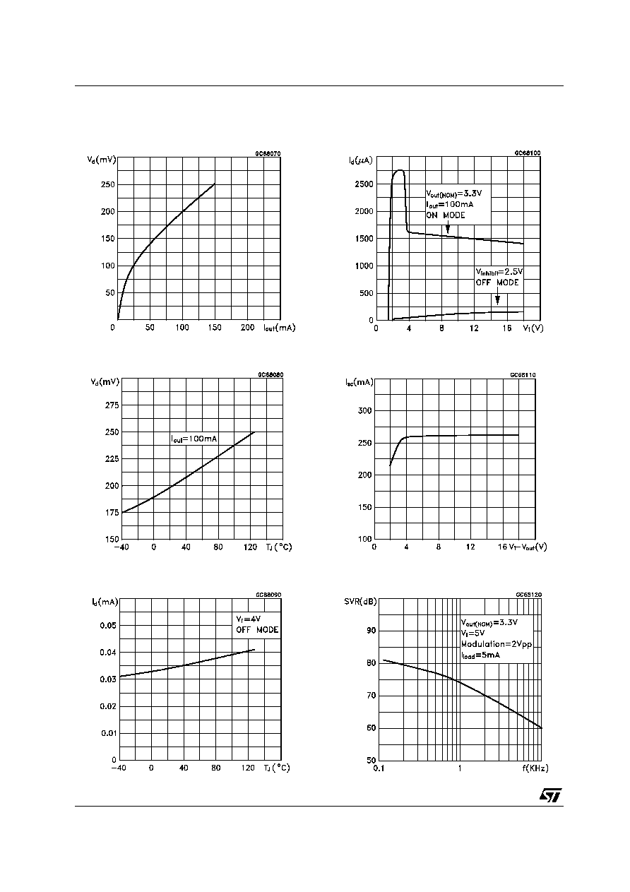
LE00AB/C SERIES
20/27
TYPICAL PERFORMANCE CHARACTERISTICS (unless otherwise specified V
O(NOM)
= 3.3 V)
Figure 3: Dropout Voltage vs Output Current
Figure 4: Dropout Voltage vs Temperature
Figure 5: Supply Current vs Temperature
Figure 6: Supply Current vs Input Voltage
Figure 7: Short Circuit Current vs Dropout
Voltage
Figure 8: S.V.R. vs Frequency
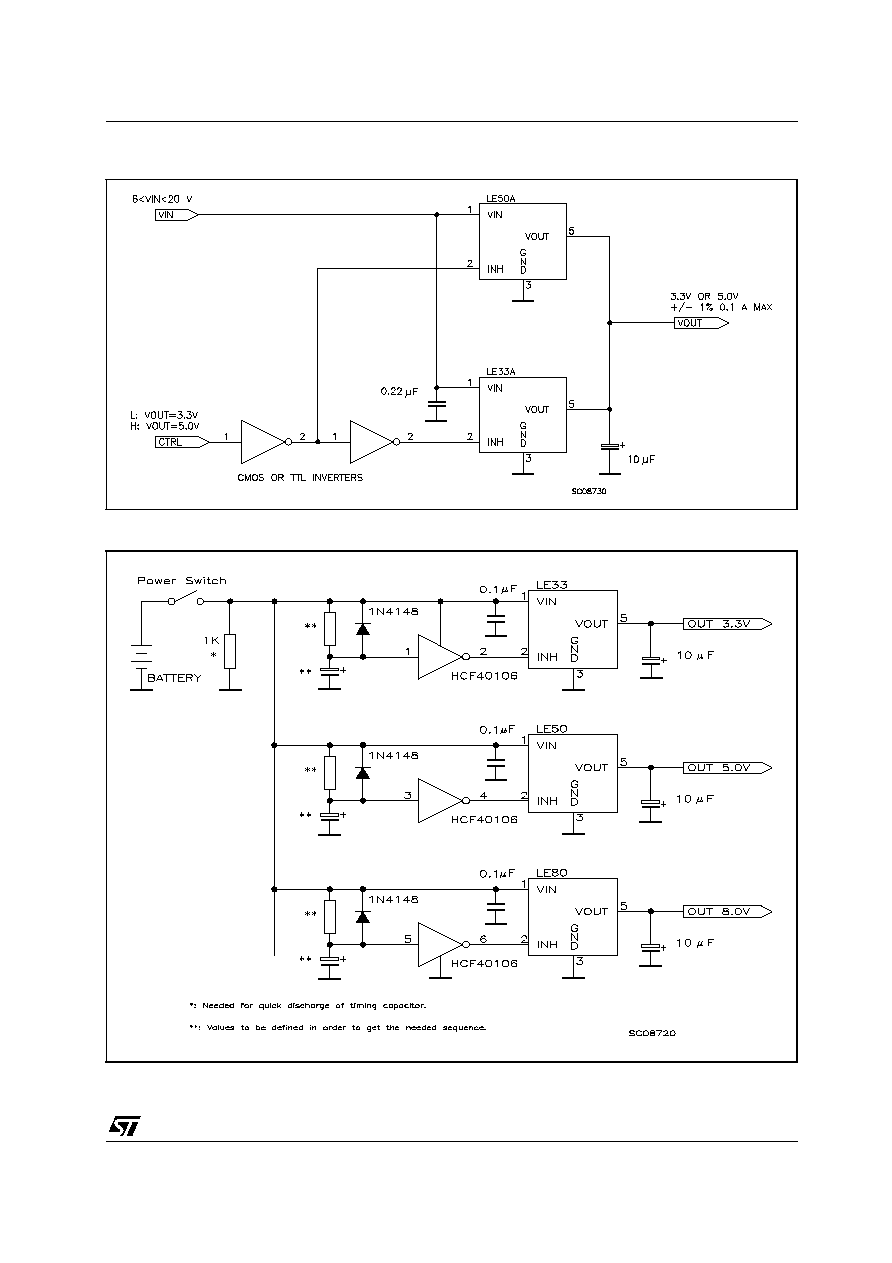
LE00AB/C SERIES
21/27
Figure 9: Logic Controlled Precision 3.3/5.0V Selectable Output
Figure 10: Sequential Multi-Output Supply
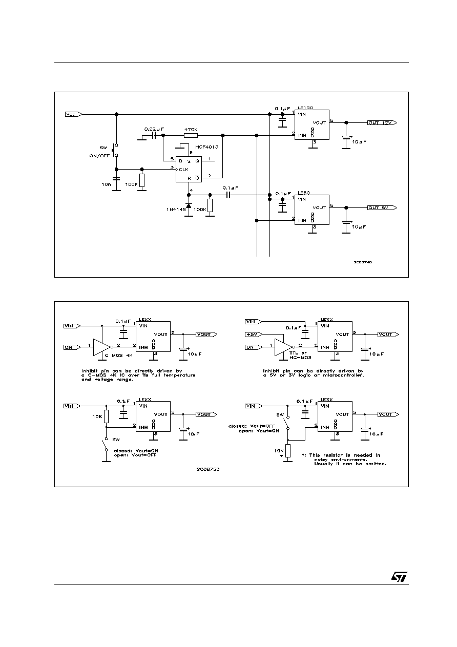
LE00AB/C SERIES
22/27
Figure 11: Multiple Supply With ON/OFF Toggle Switch
Figure 12: Basic Inhibit Functions

LE00AB/C SERIES
23/27
DIM.
mm.
inch
MIN.
TYP
MAX.
MIN.
TYP.
MAX.
A
1.35
1.75
0.053
0.069
A1
0.10
0.25
0.04
0.010
A2
1.10
1.65
0.043
0.065
B
0.33
0.51
0.013
0.020
C
0.19
0.25
0.007
0.010
D
4.80
5.00
0.189
0.197
E
3.80
4.00
0.150
0.157
e
1.27
0.050
H
5.80
6.20
0.228
0.244
h
0.25
0.50
0.010
0.020
L
0.40
1.27
0.016
0.050
k
∞ (max.)
ddd
0.1
0.04
SO-8 MECHANICAL DATA
0016023/C
8

LE00AB/C SERIES
24/27
DIM.
mm.
mils
MIN.
TYP
MAX.
MIN.
TYP.
MAX.
A
4.32
4.95
170.1
194.9
b
0.36
0.51
14.2
20.1
D
4.45
4.95
175.2
194.9
E
3.30
3.94
129.9
155.1
e
2.41
2.67
94.9
105.1
e1
1.14
1.40
44.9
55.1
L
12.7
15.49
500.0
609.8
R
2.16
2.41
85.0
94.9
S1
0.92
1.52
36.2
59.8
W
0.41
0.56
16.1
22.0
TO-92 MECHANICA DATA
0102782/C
LE00AB/C SERIES
25/27
DIM.
mm.
inch
MIN.
TYP
MAX.
MIN.
TYP.
MAX.
A
330
12.992
C
12.8
13.2
0.504
0.519
D
20.2
0.795
N
60
2.362
T
22.4
0.882
Ao
8.1
8.5
0.319
0.335
Bo
5.5
5.9
0.216
0.232
Ko
2.1
2.3
0.082
0.090
Po
3.9
4.1
0.153
0.161
P
7.9
8.1
0.311
0.319
Tape & Reel SO-8 MECHANICAL DATA
LE00AB/C SERIES
26/27
Table 36: Revision History
Date
Revision
Description of Changes
09-Jul-2004
6
I
O
typ. and max. are changed in tab. 24 and 25 - pag 14.

LE00AB/C SERIES
27/27
Information furnished is believed to be accurate and reliable. However, STMicroelectronics assumes no responsibility for the
consequences of use of such information nor for any infringement of patents or other rights of third parties which may result from
its use. No license is granted by implication or otherwise under any patent or patent rights of STMicroelectronics. Specifications
mentioned in this publication are subject to change without notice. This publication supersedes and replaces all information
previously supplied. STMicroelectronics products are not authorized for use as critical components in life support devices or
systems without express written approval of STMicroelectronics.
The ST logo is a registered trademark of STMicroelectronics
All other names are the property of their respective owners
© 2004 STMicroelectronics - All Rights Reserved
STMicroelectronics GROUP OF COMPANIES
Australia - Belgium - Brazil - Canada - China - Czech Republic - Finland - France - Germany - Hong Kong - India - Israel - Italy - Japan -
Malaysia - Malta - Morocco - Singapore - Spain - Sweden - Switzerland - United Kingdom - United States.
http://www.st.com