 | –≠–ª–µ–∫—Ç—Ä–æ–Ω–Ω—ã–π –∫–æ–º–ø–æ–Ω–µ–Ω—Ç: LK112XX44 | –°–∫–∞—á–∞—Ç—å:  PDF PDF  ZIP ZIP |
1/12
June 2003
s
OUTPUT CURRENT UP TO 150mA
s
LOW DROPOUT VOLTAGE (350mV AT
I
OUT
=150mA)
s
VERY LOW QUIESCENT CURRENT: 0.1
µ
A
IN OFF MODE AND MAX 250
µ
A IN ON
MODE AT I
OUT
=0mA
s
LOW OUTPUT NOISE: TYP 30
µ
V AT
I
OUT
=60mA AND 10Hz<f<80KHz
s
WIDE RANGE OF OUTPUT VOLTGAES
s
INTERNAL CURRENT AND THERMAL LIMIT
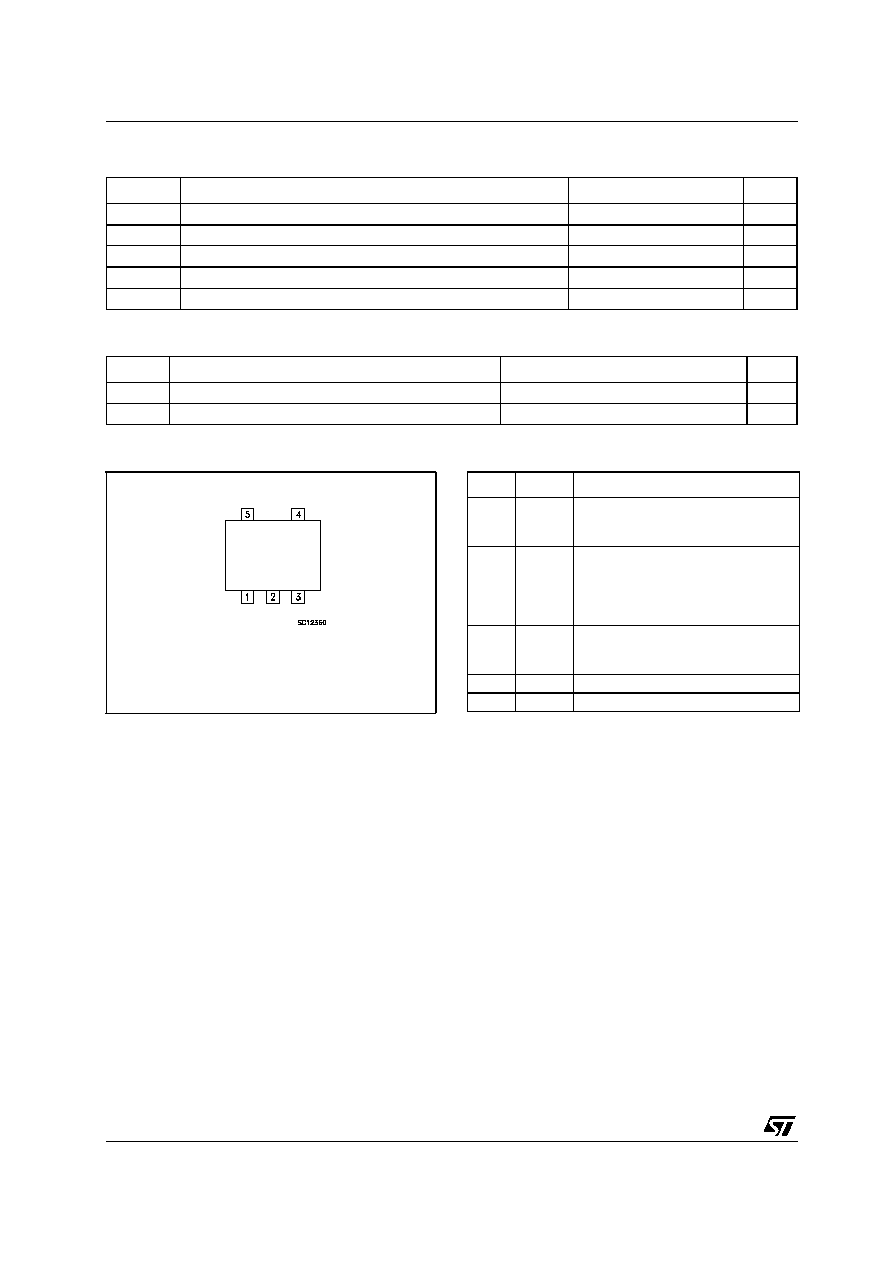
DESCRIPTION
The LK112 is a low dropout linear regulator with a
built in electronic switch. The internal switch can
be controlled by TTL or CMOS logic levels. The
device is ON state when the control pin is pulled to
a logic high level. An external capacitor can be
used connected to the noise bypass pin to lower
the output noise level to 30
µ
V
rms
. An internal PNP
pass transistor is used to achieve a low dropout
voltage.
The LK112 has a very low quiescent current in ON
MODE while in OFF MODE the Iq is reduced
down to 100nA max. The internal thermal
shutdown circuitry limits the juntion temperature to
below 150∞C. The load current is internally
monitored and the device will shutdown in the
presence of a short circuit or overcurrent condition
at the output.
LK112
SERIES
LOW NOISE LOW DROP VOLTAGE REGULATOR
WITH SHUTDOWN FUNCTION
SCHEMATIC DIAGRAM
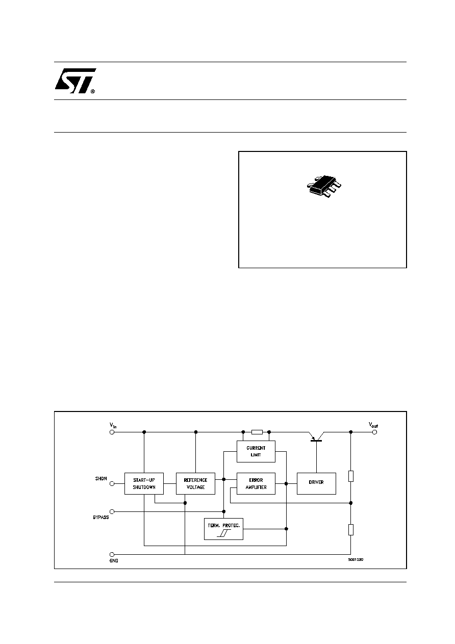
SOT23-5L
LK112 SERIES
2/12
ABSOLUTE MAXIMUM RATINGS
THERMAL DATA
CONNECTION DIAGRAM (top view)
PIN DESCRIPTION
Symbol
Parameter≤
Value
Unit
V
I
DC Input Voltage
16
V
V
SHDN
Shutdown Input Voltage
16
V
I
O
Output Current
Internally limited
T
stg
Storage Temperature Range
-55 to +150
∞C
T
op
Operating Junction Temperature Range
-30 to +125
∞C
Symbol
Parameter
SOT23-5L
Unit
R
thj-case
Thermal Resistance Junction-case
81
∞C/W
R
thj-amb
Thermal Resistance Junction-ambient
255
∞C/W
SOT23-5L
Pin N∞ Symbol
Name and Function
1
SHDN
Shutdown Input: Disables the
regulator when is connected to GND
or to positive voltage less than 0.6V
2
GND
Ground Pin: Internally connected to
the die attach flag to decrease the
total thermal resistance and increase
the package ability to dissipate
power.
3
Bypass Bypass Pin: Bypass with 0.1
µ
F to
improve the Vref thermal noise
performances.
4
OUT
Output Port
5
IN
Input Port
LK112 SERIES
3/12
ELECTRICAL CHARACTERISTICS FOR LK112 (T
j
= 25∞C, V
IN
=V
OUT
+1V (see Note 1), I
OUT
=0mA,
V
SHDN
=1.8V, C
I
= 1
µ
F, C
O
= 2.2
µ
F, C
BYPASS
= 0.1
µ
F unless otherwise specified)
Note 1: for version with output voltage less than 2V V
IN
=2.4V
Note 2: only for version with output voltage more than 2.1V
Symbol
Parameter
Test Conditions
Min.
Typ.
Max.
Unit
I
d
Quiescent Current
ON MODE (except I
SHDN
)
175
250
µ
A
OFF MODE V
I
= 8V
V
SHDN
= 0V
0
0.1
µ
A
V
O
Output Voltage
I
O
= 30mA
(see table)
V
O
Line Regulation
V
I
= V
O
+1V to V
O
+6V,
V
O
5.6V
0.7
20
mV
V
I
= V
O
+1V to V
O
+6V,
V
O
>
5.6V
0.8
40
mV
V
O
Load Regulation
I
O
= 1 to 60mA
15
30
mV
I
O
= 1 to 150mA
25
90
mV
V
d
Dropout Voltage
I
O
= 60 mA (see Note 2)
0.17
0.24
V
I
O
= 150 mA (see Note 2)
0.29
0.35
V
I
O
Output Current Limit
150
mA
SVR
Supply Voltage Rejection
V
I
= V
O
+1.5V
C
BYP
= 0.1
µ
F
C
O
= 10
µ
F
f = 400Hz
I
O
= 30mA
55
dB
eN
Output Noise Voltage
B= 10Hz to 80KHz C
BYP
= 0.1
µ
F
C
O
= 10
µ
F
V
I
= V
O
+1.5V,I
O
= 60mA
30
µ
Vrms
I
SHDN
Shutdown Input Current
V
SHDN
= 1.8V
Output ON
12
35
µ
A
V
SHDN
Shutdown Input Logic
Output ON
Output OFF
1.8
0.6
V
V
V
O
/T
j
Output Voltage
Temperature Coefficient
I
O
= 10mA
0.09
mV/∞C

LK112 SERIES
4/12
ORDERING NUMBERS AND OUTPUT VOLTAGE
(*) Available on request
Part Number
Output Voltage
V
OUT
Min
V
OUT
Max
Test Voltage
LK112M13TR
1.3V
1.24V
1.36V
2.4V
LK112M14TR (*)
1.4V
1.34V
1.46V
2.4V
LK112M15TR
1.5V
1.44V
1.56V
2.4V
LK112M16TR
1.6V
1.54V
1.66V
2.4V
LK112M17TR
1.7V
1.64V
1.76V
2.4V
LK112M18TR
1.8V
1.74V
1.86V
2.4V
LK112M19TR (*)
1.9V
1.84V
1.96V
2.4V
LK112M20TR (*)
2.0V
1.94V
2.06V
3.0V
LK112M21TR
2.1V
2.04V
2.16V
3.1V
LK112M22TR (*)
2.2V
2.14V
2.26V
3.2V
LK112M23TR (*)
2.3V
2.24V
2.36V
3.3V
LK112M24TR (*)
2.4V
2.34V
2.46V
3.4V
LK112M25TR
2.5V
2.44V
2.56V
3.5V
LK112M26TR (*)
2.6V
2.54V
2.66V
3.6V
LK112M27TR (*)
2.7V
2.64V
2.76V
3.7V
LK112M28TR
2.8V
2.74V
2.86V
3.8V
LK112M29TR (*)
2.9V
2.84V
2.96V
3.9V
LK112M30TR
3.0V
2.94V
3.06V
4.0V
LK112M31TR (*)
3.1V
3.04V
3.16V
4.1V
LK112M32TR
3.2V
3.14V
3.26V
4.2V
LK112M33TR
3.3V
3.24V
3.36V
4.3V
LK112M34TR (*)
3.4V
3.335V
3.465V
4.4V
LK112M35TR (*)
3.5V
3.435V
3.565V
4.5V
LK112M36TR
3.6V
3.535V
3.655V
4.6V
LK112M37TR (*)
3.7V
3.630V
3.770V
4.7V
LK112M38TR
3.8V
3.725V
3.875V
4.8V
LK112M39TR (*)
3.9V
3.825V
3.975V
4.9V
LK112M40TR
4.0V
3.920V
4.080V
5.0V
LK112M41TR (*)
4.1V
4.020V
4.180V
5.1V
LK112M42TR (*)
4.2V
4.120V
4.280V
5.2V
LK112M43TR (*)
4.3V
4.215V
4.385V
5.3V
LK112M44TR (*)
4.4V
4.315V
4.485V
5.4V
LK112M45TR (*)
4.5V
4.410V
4.590V
5.5V
LK112M46TR (*)
4.6V
4.510V
4.690V
5.6V
LK112M47TR
4.7V
4.605V
4.795V
5.7V
LK112M48TR (*)
4.8V
4.705V
4.895V
5.8V
LK112M49TR (*)
4.9V
4.800V
5.000V
5.9V
LK112M50TR
5.0V
4.900V
5.100V
6.0V
LK112M55TR (*)
5.5V
5.390V
5.610V
6.5V
LK112M60TR
6.0V
5.880V
6.120V
7.0V
LK112M80TR
8.0V
7.840V
8.160V
9.0V
LK112 SERIES
5/12
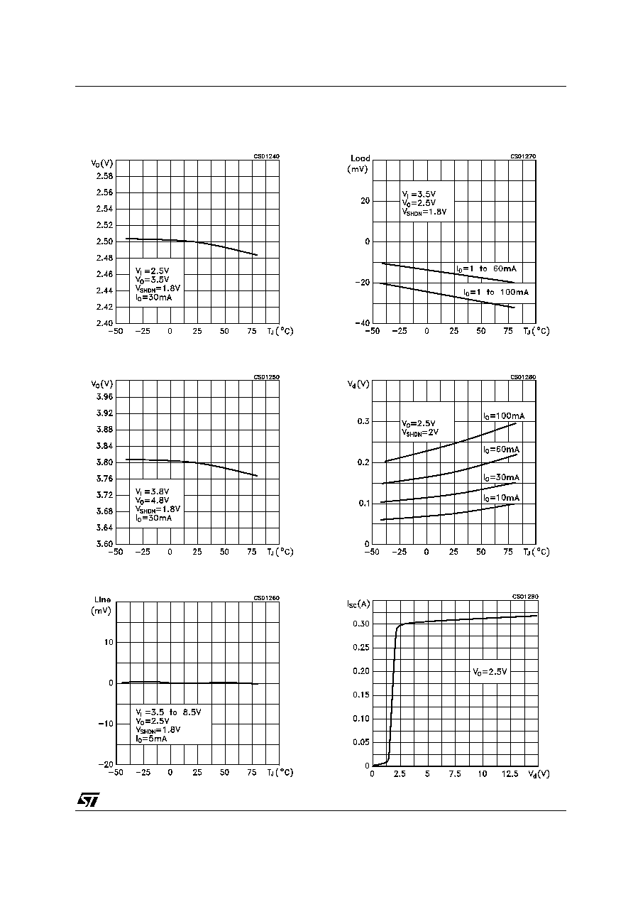
TYPICAL CHARACTERISTICS (unless otherwise specified T
j
= 25∞C, C
I
=1
µ
F, C
O
=2.2
µ
F, C
BYP
=100nF)
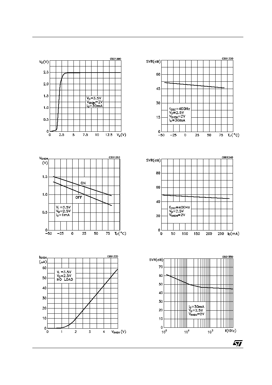
Figure 1 : Output Voltage vs Temperature
Figure 2 : Output Voltage vs Temperature
Figure 3 : Line Regulation vs Temperature
Figure 4 : Load Regulation vs Temperature
Figure 5 : Dropout Voltage vs Temperature
Figure 6 : Short Circuit Currennt vs Dropout
Voltage
LK112 SERIES
6/12
Figure 7 : Output Voltage vs Input Voltage
Figure 8 : Shutdown Voltage vs Temperature
Figure 9 : Shutdown Current vs Shutdown
Voltage
Figure 10 : Supply Voltage Rejection vs
Temperature
Figure 11 : Supply Voltage Rejection vs Output
Current
Figure 12 : Supply Voltage Rejection vs
Frequency
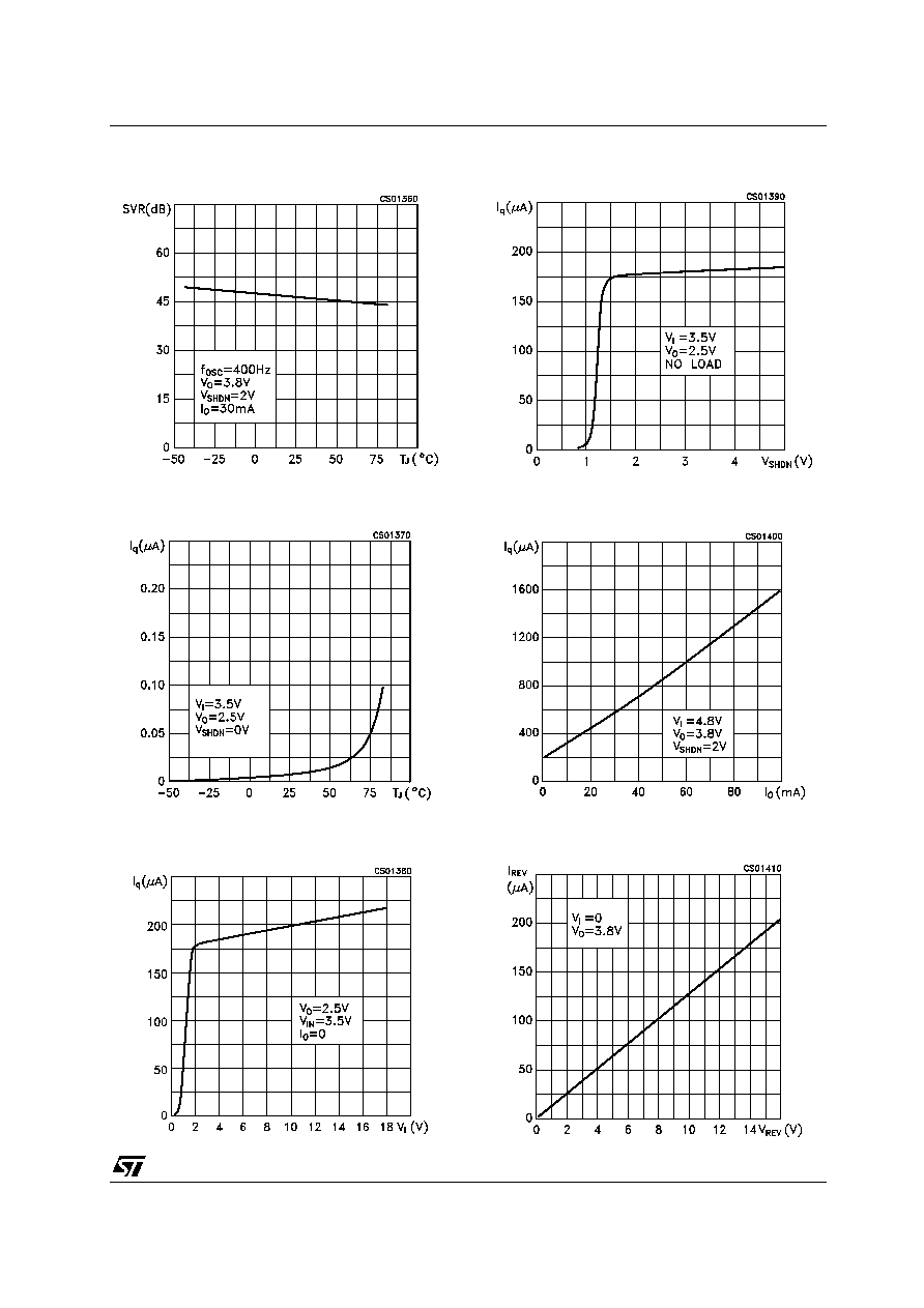
LK112 SERIES
7/12
Figure 13 : Supply Voltage Rejection vs
Temperature
Figure 14 : Quiescent Current vs Temperature
Figure 15 : Quiescent Current vs Input Voltage
Figure 16 : Quiescent Current vs Shutdown
Voltage
Figure 17 : Quiescent Current vs Output Current
Figure 18 : Reverse Current vs Reverse Voltage
LK112 SERIES
8/12
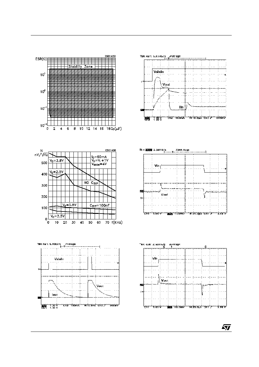
Figure 19 : Stability
Figure 20 : Spectrum Noise
Figure 21 : Start-up Transient
Figure 22 : Start-up Transient
Figure 23 : Line Transient
Figure 24 : Line Transient
V
I
=3.5V, V
O
=2.5V, V
SHDN
= 0 to 1.8V, R
L
=2.5K
, C
I
=1
µ
F,
C
O
=4.7
µ
F, C
BY
=10nF
V
I
=3.5V, V
O
=2.5V, V
SHDN
= 0 to 1.8V, R
L
=68
, C
I
=1
µ
F, C
O
=4.7
µ
F,
C
BY
=100nF
V
I
=3.5 to 4.5V, V
O
=2.5V, V
SHDN
=1.8V, I
O
=30mA, No C
I
, C
O
=10
µ
F,
C
BY
=100nF, t
s
=t
f
=2
µ
s
V
I
=3.5 to 4.5V, V
O
=2.5V, V
SHDN
=1.8V, I
O
=30mA, No C
I
, C
O
=10
µ
F,
C
BY
=10nF, t
s
=t
f
=2
µ
s
LK112 SERIES
9/12
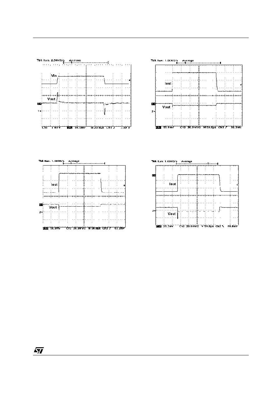
Figure 25 : Line Transient
Figure 26 : Load Transient
Figure 27 : Load Transient
Figure 28 : Load Transient
V
I
=3.5 to 4.5V, V
O
=2.5V, V
SHDN
=1.8V, I
O
=30mA, No C
I
, C
O
=1
µ
F,
C
BY
=1nF, t
s
=t
f
=2
µ
s
V
I
=3.5 V, V
O
=2.5V, V
SHDN
=1.8V, I
O
=50 to 100mA, C
I
=1
µ
F,
C
O
=2.2
µ
F, C
BY
=10nF, t
s
=t
f
=250ns
V
I
=3.5V, V
O
=2.5V, V
SHDN
=1.8V, I
O
=50 to 100mA, C
I
1
µ
F,
C
O
=10
µ
F, C
BY
=100nF, t
s
=t
f
=250ns
V
I
=4.8 V, V
O
=3.8V, V
SHDN
=1.8V, I
O
=50 to 100mA, C
I
=1
µ
F,
C
O
=2.2
µ
F, C
BY
=10nF, t
s
=t
f
=250ns
LK112 SERIES
10/12
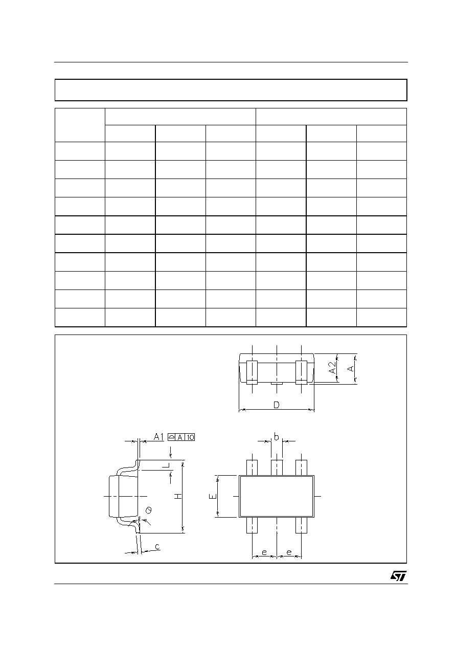
DIM.
mm.
mils
MIN.
TYP
MAX.
MIN.
TYP.
MAX.
A
0.90
1.45
35.4
57.1
A1
0.00
0.10
0.0
3.9
A2
0.90
1.30
35.4
51.2
b
0.35
0.50
13.7
19.7
C
0.09
0.20
3.5
7.8
D
2.80
3.00
110.2
118.1
E
1.50
1.75
59.0
68.8
e
0.95
37.4
H
2.60
3.00
102.3
118.1
L
0.10
0.60
3.9
23.6
SOT23-5L MECHANICAL DATA
7049676C
.

LK112 SERIES
11/12
DIM.
mm.
inch
MIN.
TYP
MAX.
MIN.
TYP.
MAX.
A
180
7.086
C
12.8
13.0
13.2
0.504
0.512
0.519
D
20.2
0.795
N
60
2.362
T
14.4
0.567
Ao
3.13
3.23
3.33
0.123
0.127
0.131
Bo
3.07
3.17
3.27
0.120
0.124
0.128
Ko
1.27
1.37
1.47
0.050
0.054
0.0.58
Po
3.9
4.0
4.1
0.153
0.157
0.161
P
3.9
4.0
4.1
0.153
0.157
0.161
Tape & Reel SOT23-xL MECHANICAL DATA

LK112 SERIES
12/12
Information furnished is believed to be accurate and reliable. However, STMicroelectronics assumes no responsibility for the
consequences of use of such information nor for any infringement of patents or other rights of third parties which may result from
its use. No license is granted by implication or otherwise under any patent or patent rights of STMicroelectronics. Specifications
mentioned in this publication are subject to change without notice. This publication supersedes and replaces all information
previously supplied. STMicroelectronics products are not authorized for use as critical components in life support devices or
systems without express written approval of STMicroelectronics.
© The ST logo is a registered trademark of STMicroelectronics
© 2003 STMicroelectronics - Printed in Italy - All Rights Reserved
STMicroelectronics GROUP OF COMPANIES
Australia - Brazil - Canada - China - Finland - France - Germany - Hong Kong - India - Israel - Italy - Japan - Malaysia - Malta - Morocco
Singapore - Spain - Sweden - Switzerland - United Kingdom - United States.
© http://www.st.com