Rev 3
July 2005
1/16
16
LM158-LM258-LM358
LM158A-LM258A-LM358A
Low Power Dual Operational Amplifiers
Internally frequency compensated
Large DC voltage gain: 100dB
Wide bandwidth (unity gain): 1.1mHz
(temperature compensated)
Very low supply current/op (500µA) essentially
independent of supply voltage
Low input bias current: 20nA
(temperature compensated)
Low input offset voltage: 2mV
Low input offset current: 2nA
Input common-mode voltage range includes
ground
Differential input voltage range equal to the
power supply voltage
Large output voltage swing 0V to (Vcc - 1.5V)
Description
These circuits consist of two independent, high-
gain, internally frequency-compensated which
were designed specifically to operate from a
single power supply over a wide range of voltages.
The low power supply drain is independent of the
magnitude of the power supply voltage.
Application areas include transducer amplifiers,
DC gain blocks and all the conventional op-amp
circuits which now can be more easily
implemented in single power supply systems. For
example, these circuits can be directly supplied
with the standard +5V which is used in logic
systems and will easily provide the required
interface electronics without requiring any
additional power supply.
In the linear mode the input common-mode
voltage range includes ground and the output
voltage can also swing to ground, even though
operated from only a single power supply voltage.
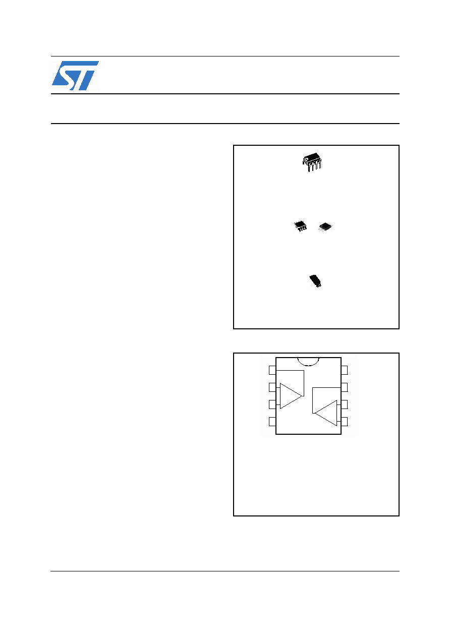
Pin Connections (top view)
N
DIP-8
(Plastic Package)
D & S
SO-8 & miniSO-8
(Plastic Micropackage)
P
TSSOP8
(Thin Shrink Small Outline Package)
1
2
3
4
5
6
7
8
-
+
-
+
1 - Output 1
2 - Inverting input
3 - Non-inverting input
4 - V
CC
-
5 - Non-inverting input 2
6 - Inverting input 2
7 - Output 2
8 - V
CC
+
www.st.com
LM158-LM258-LM358-LM158A-LM258A-LM358A
2/16
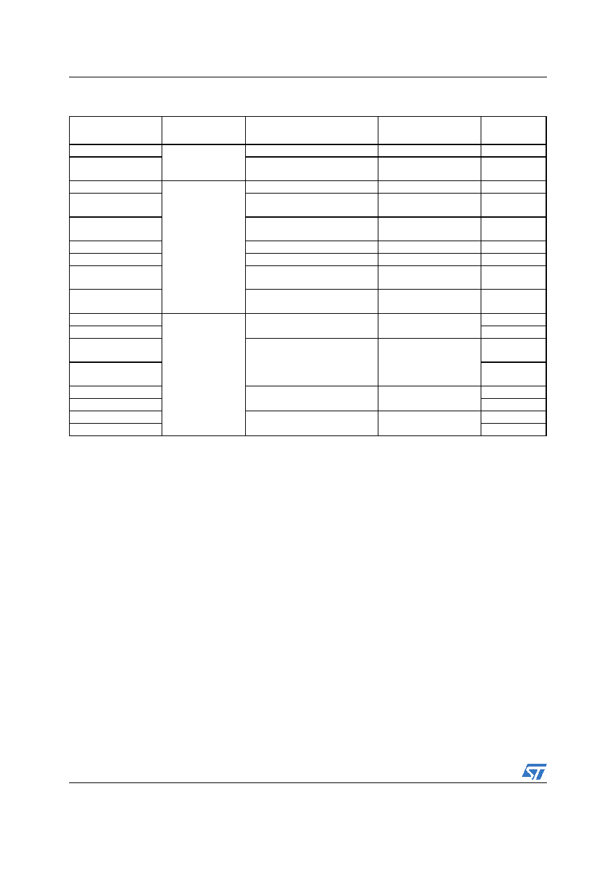
Order Codes
Part Number
Temperature
Range
Package
Packaging
Marking
LM158N
-55∞C, +125∞C
DIP-8
Tube
LM158N
LM158D
LM158DT
SO-8
Tube or Tape & Reel
158
LM258AN
-40∞C, +105∞C
DIP-8
Tube
LM258A
LM258AD
LM258ADT
SO-8
Tube or Tape & Reel
258A
LM258APT
TSSOP-8
(Thin Shrink Outline Package)
Tape & Reel
258A
LM258AST
miniSO-8
Tape & Reel
K408
LM258N
DIP-8
Tube
LM258N
LM258D
LM258DT
SO-8
Tube or Tape & Reel
258
LM258PT
TSSOP-8
(Thin Shrink Outline Package)
Tape & Reel
258
LM358N
0∞C, +70∞C
DIP-8
Tube
LM358N
LM358AN
LM358AN
LM358D
LM358DT
SO-8
Tube or Tape & Reel
358
LM358AD
LM358ADT
358A
LM358PT
TSSOP-8
(Thin Shrink Outline Package)
Tape & Reel
358
LM358APT
358A
LM358ST
miniSO-8
Tape & Reel
K405
LM358AST
K404

LM158-LM258-LM358-LM158A-LM258A-LM358A
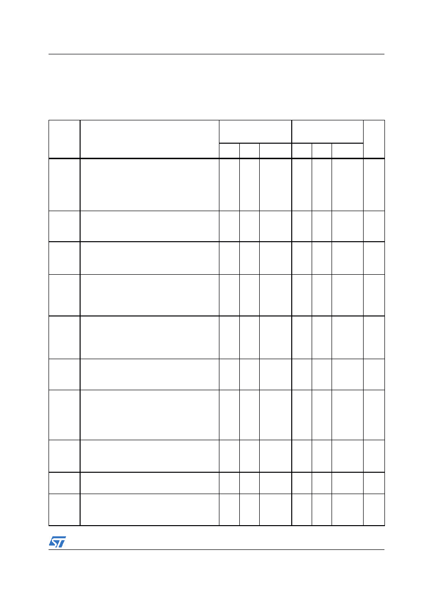
Absolute Maximum Ratings
3/16
1
Absolute Maximum Ratings
Table 1.
Key parameters and their absolute maximum ratings
Symbol
Parameter
LM158,A
LM258,A
LM358,A
Unit
V
CC
Supply voltage
+/-16 or 32
V
Vi
Input Voltage
-0.3 to +32
V
V
id
Differential Input Voltage
+32
V
P
tot
Power Dissipation
(1)
1.
Power dissipation must be considered to ensure maximum junction temperature (Tj) is not exceeded.
500
mW
Output Short-circuit Duration
(2)
2.
Short-circuits from the output to V
CC
can cause excessive heating if V
CC
> 15V. The maximum output current
is approximately 40mA independent
of the magnitude of V
CC
. Destructive dissipation can result from simultaneous short-circuit on all amplifiers.
Infinite
I
in
Input Current
(3)
3.
This input current only exists when the voltage at any of the input leads is driven negative. It is due to the
collector-base junction of the input PNP
transistor becoming forward biased and thereby acting as input diodes clamps. In addition to this diode action,
there is also NPN parasitic action on
the IC chip. this transistor action can cause the output voltages of the Op-amps to go to the V
CC
voltage level
(or to ground for a large overdrive)
for the time duration than an input is driven negative.
This is not destructive and normal output will set up again for input voltage higher than -0.3V.
50
mA
T
oper
Operating Free-air Temperature Range
-55 to +125 -40 to +105
0 to +70
∞C
T
stg
Storage Temperature Range
-65 to +150
∞C
T
j
Maximum Junction Temperature
150
∞C
R
thja
Thermal Resistance Junction to Ambient
(4)
SO8
TSSOP8
DIP8
miniSO8
4.
Short-circuits can cause excessive heating. Destructive dissipation can result from simultaneous short-circuit
on all amplifiers
125
120
85
190
∞C/W
ESD
HBM: Human Body Model
(5)
5.
Human body model, 100pF discharged through a 1.5k
resistor into pin of device.
300
V
MM: Machine Model
(6)
6.
Machine model ESD, a 200pF cap is charged to the specified voltage, then discharged directly into the IC with
no external series resistor (internal resistor < 5
), into pin to pin of device.
200
V
CDM: Charged Device Model
1.5
kV
LM158-LM258-LM358-LM158A-LM258A-LM358A
Electrical Characteristics
5/16
3 Electrical
Characteristics
Table 2.
Electrical characteristics for V
CC
+
= +5V, V
CC
-
= Ground, V
o
= 1.4V, T
amb
= +25∞C (unless
otherwise specified)
Symbol
Parameter
LM158A-LM258A
LM358A
LM158-LM258
LM358
Unit
Min.
Typ.
Max.
Min.
Typ.
Max.
V
io
Input Offset Voltage - note
(1)
T
amb
= +25∞C
LM158, LM258
LM158A
T
min
T
amb
T
max
LM158, LM258
1
3
2
4
2
7
5
9
7
mV
I
io
Input Offset Current
T
amb
= +25∞C
T
min
T
amb
T
max
2
10
30
2
30
40
nA
I
ib
Input Bias Current - note
(2)
T
amb
= +25∞C
T
min
T
amb
T
max
20
50
100
20
150
200
nA
A
vd
Large Signal Voltage Gain
V
CC
= +15V, R
L
= 2k
, V
o
= 1.4V to 11.4V
T
amb
= +25∞C
T
min
T
amb
T
max
50
25
100
50
25
100
V/mV
SVR
Supply Voltage Rejection Ratio (R
s
10k)
V
CC
+
= 5V to 30V
T
amb
= +25∞C
T
min
T
amb
T
max
65
65
100
65
65
100
dB
I
CC
Supply Current, all Amp, no load
T
min
T
amb
T
max
V
CC
= +5V
T
min
T
amb
T
max
V
CC
= +30V
0.7
1.2
2
0.7
1.2
2
mA
V
icm
Input Common Mode Voltage Range
V
CC
= +30V - note
(3)
T
amb
= +25∞C
T
min
T
amb
T
max
0
0
V
CC
+
-
1.5
V
CC
+
-2
0
0
V
CC
+
-
1.5
V
CC
+
-2
V
CMR
Common Mode Rejection Ratio (R
s
10k)
T
amb
= +25∞C
T
min
T
amb
T
max
70
60
85
70
60
85
dB
I
source
Output Current Source
V
CC
= +15V, V
o
= +2V, V
id
= +1V
20
40
60
20
40
60
mA
I
sink
Output Sink Current (V
id
= -1V)
V
CC
= +15V, V
o
= +2V
V
CC
= +15V, V
o
= +0.2V
10
12
20
50
10
12
20
50
mA
µA