 | –≠–ª–µ–∫—Ç—Ä–æ–Ω–Ω—ã–π –∫–æ–º–ø–æ–Ω–µ–Ω—Ç: LM193WD | –°–∫–∞—á–∞—Ç—å:  PDF PDF  ZIP ZIP |

1/10
s
WIDE SINGLE SUPPLY VOLTAGE RANGE
OR DUAL SUPPLIES : +2V TO +36V OR ±1V
TO ±18V
s
VERY LOW SUPPLY CURRENT (0.4mA)
INDEPENDENT OF SUPPLY VOLTAGE
(1mW/comparator at +5V)
s
LOW INPUT BIAS CURRENT : 25nA TYP
s
LOW INPUT OFFSET CURRENT : ±5nA TYP
s
LOW INPUT OFFSET VOLTAGE : ±1mV TYP
s
INPUT COMMON-MODE VOLTAGE RANGE
INCLUDES GROUND
s
LOW OUTPUT SATURATION VOLTAGE :
250mV TYP. (Io = 4mA)
s
DIFFERENTIAL INPUT VOLTAGE RANGE
EQUAL TO THE SUPPLY VOLTAGE
s
TTL, DTL, ECL, MOS, CMOS COMPATIBLE
OUTPUTS
s
ESD INTERNAL PROTECTION: 2kV
DESCRIPTION
These devices consist of two independent low
voltage comparators designed specifically to oper-
ate from a single supply over a wide range of volt-
ages. Operation from split power supplies is also
possible.
These comparators also have a unique character-
istic in that the input common-mode voltage range
includes ground even though operated from a sin-
gle power supply voltage.
All the pins are protected against electrostatic dis-
charge up to 2kV. As a consequence, the input
voltages must not exceed the magnitude of Vcc+
or Vcc-.
ORDER CODE
N = Dual in Line Package (DIP)
D = Small Outline Package (SO) - also available in Tape & Reel (DT)
P = Thin Shrink Small Outline Package (TSSOP) - only available in Tape
&Reel (PT)
PIN CONNECTIONS (top view)
Part
Number
Temperature
Range
Package
N
D
P
LM193W
-55∞C, +125∞C
∑
∑
∑
LM293W
-40∞C, +105∞C
∑
∑
∑
LM393W
0∞C, +70∞C
∑
∑
∑
Example : LM393WD
D
SO8
(Plastic Micropackage)
N
DIP8
(Plastic Package)
P
TSSOP8
(Thin Shrink Small Outline Package)
1 - Output 1
2 - Inverting input 1
3 - Non-inverting input 1
4 - V
CC
-
5 - Non-inverting input 2
6 - Inverting input 2
7 - Output 2
8 - V
CC
+
LM193W - LM293W
LM393W
LOW POWER DUAL VOLTAGE COMPARATORS
May 2004
LM193W - LM293W - LM393W
2/10
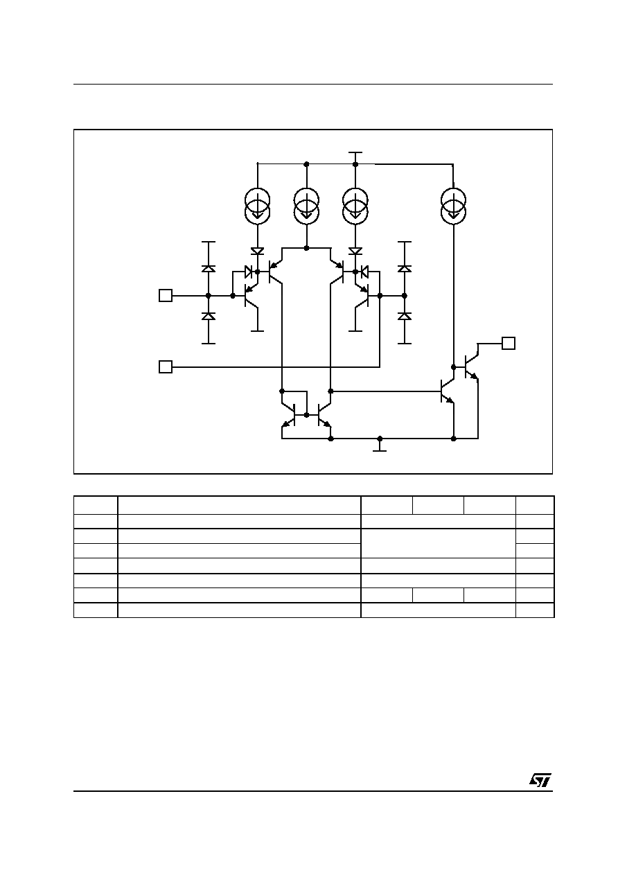
SCHEMATIC DIAGRAM (1/2 LM193)
ABSOLUTE MAXIMUM RATINGS
Symbol
Parameter
LM193W
LM293W
LM393W
Unit
V
CC
Supply voltage
±18 or 36
V
V
id
Differential Input Voltage
V
CC
-
-0.3 to V
CC
+
+0.3
V
V
i
Input Voltage
V
Output Short-circuit to Ground - note
1)
1.
Short-circuits from the output to V
CC
+
can cause excessive heating and eventual destruction. The maximum output current is approximately 20mA
independent of the magnitude of V
CC
+
.
Infinite
P
tot
Power Dissipation
830
mW
T
oper
Opearting Free-air Temperature Range
-55 to +125 -40 to +105
0 to +70
∞C
T
stg
Storage Temperature Range
-65 to +150
∞C
VCC-
VCC-
VCC+
VCC+
VCC+
VCC-
VCC-
VCC-
3.5µA
100µA
3.5µA
100µA
Vo
Non-Inverting
Inverting
Input
Input
LM193W - LM293W - LM393W
3/10
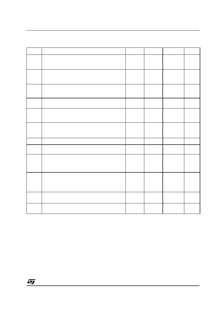
ELECTRICAL CHARACTERISTICS
V
CC
+
= +5V, V
CC
-
= 0V, T
amb
= +25∞C (unless otherwise specified)
Symbol
Parameter
Min
Typ.
Max.
Unit
V
io
Input Offset Voltage - note
1)
T
amb
= +25∞C
T
min
T
amb
T
max
1.
At output switch point, V
o
1.4V, R
s
= 0 with V
CC
+
from 5V to 30V, and over the full common-mode range (0V to V
CC
+
-1.5V).
1
5
9
mV
I
ib
Input Bias Current - note
2)
T
amb
= +25∞C
T
min
T
amb
T
max
2.
The direction of the input current is out of the IC due to the PNP input stage. This current is essentially constant, independent of the state of the
output, so no loading charge exists on the reference of input lines.
25
250
400
nA
I
io
Input Offset Current
T
amb
= +25∞C
T
min
T
amb
T
max
5
50
150
nA
A
vd
Large Signal Voltage Gain
V
CC
= 15V, R
L
= 15k
,
V
o
= 1V to 11V
50
200
V/mV
I
CC
Supply Current (all comparators)
V
CC
= 5V, no load
V
CC
= 30V, no load
0.4
1
1
2.5
mA
V
icm
Input Common Mode Voltage Range - note
3)
T
amb
= +25∞C
T
min
T
amb
T
max
3.
The input common-mode voltage of either input signal voltage should not be allowed to go negative by more than 0.3V. The upper end of the
common-mode voltage range is V
CC
+
-1.5V, but either or both inputs can go to +30V without damage
0
0
V
CC
+
-1.5
V
CC
+
-2
V
V
id
Differential Input Voltage -note
4)
4.
Positive excursions of input voltage may exceed the power supply level. As long as the other voltage remains within the common-mode range, the
comparator will provide a proper output state. The low input voltage state must not be less than -0.3V (or 0.3V bellow the negative power supply, if
used).
V
CC
+
V
Isink
Output Sink Currrent
V
id
= 1V, V
o
= 1.5V
6
16
mA
V
OL
Low Level Output Voltage
V
id
= -1V, I
sink
= 4mA
T
amb
= +25∞C
T
min
T
amb
T
max
250
400
700
mV
I
OH
High Level Output Current (V
id
= 1V)
V
id
= 1V, V
CC
= V
o
= 30V
T
amb
= +25∞C
T
min
T
amb
T
max
0.1
1
nA
µ
A
t
re
Response Time - note
5)
R
L
= 5.1k
to V
CC
+
5.
The response time specified is for a 100mV input step with 5mV overdrive. For larger overdrive signals 300ns can be obtained
1.3
µ
s
t
rel
Large Signal Response Time
V
i
= TTL, V
(ref)
= +1.4V, R
L
= 5.1k
to V
CC
+
300
ns
LM193W - LM293W - LM393W
4/10
LM193W - LM293W - LM393W
5/10
LM193W - LM293W - LM393W
6/10
LM193W - LM293W - LM393W
7/10

LM193W - LM293W - LM393W
8/10
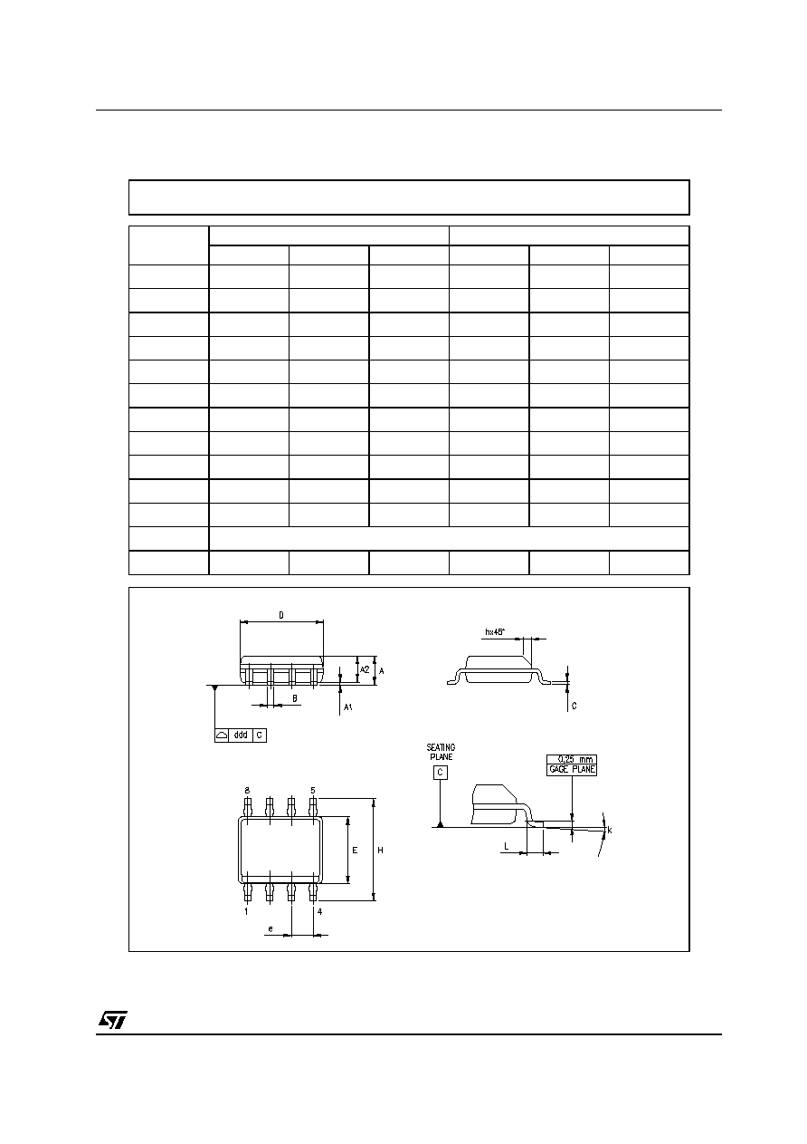
PACKAGE MECHANICAL DATA
DIM.
mm.
inch
MIN.
TYP
MAX.
MIN.
TYP.
MAX.
A
3.3
0.130
a1
0.7
0.028
B
1.39
1.65
0.055
0.065
B1
0.91
1.04
0.036
0.041
b
0.5
0.020
b1
0.38
0.5
0.015
0.020
D
9.8
0.386
E
8.8
0.346
e
2.54
0.100
e3
7.62
0.300
e4
7.62
0.300
F
7.1
0.280
I
4.8
0.189
L
3.3
0.130
Z
0.44
1.6
0.017
0.063
Plastic DIP-8 MECHANICAL DATA
P001F
LM193W - LM293W - LM393W
9/10
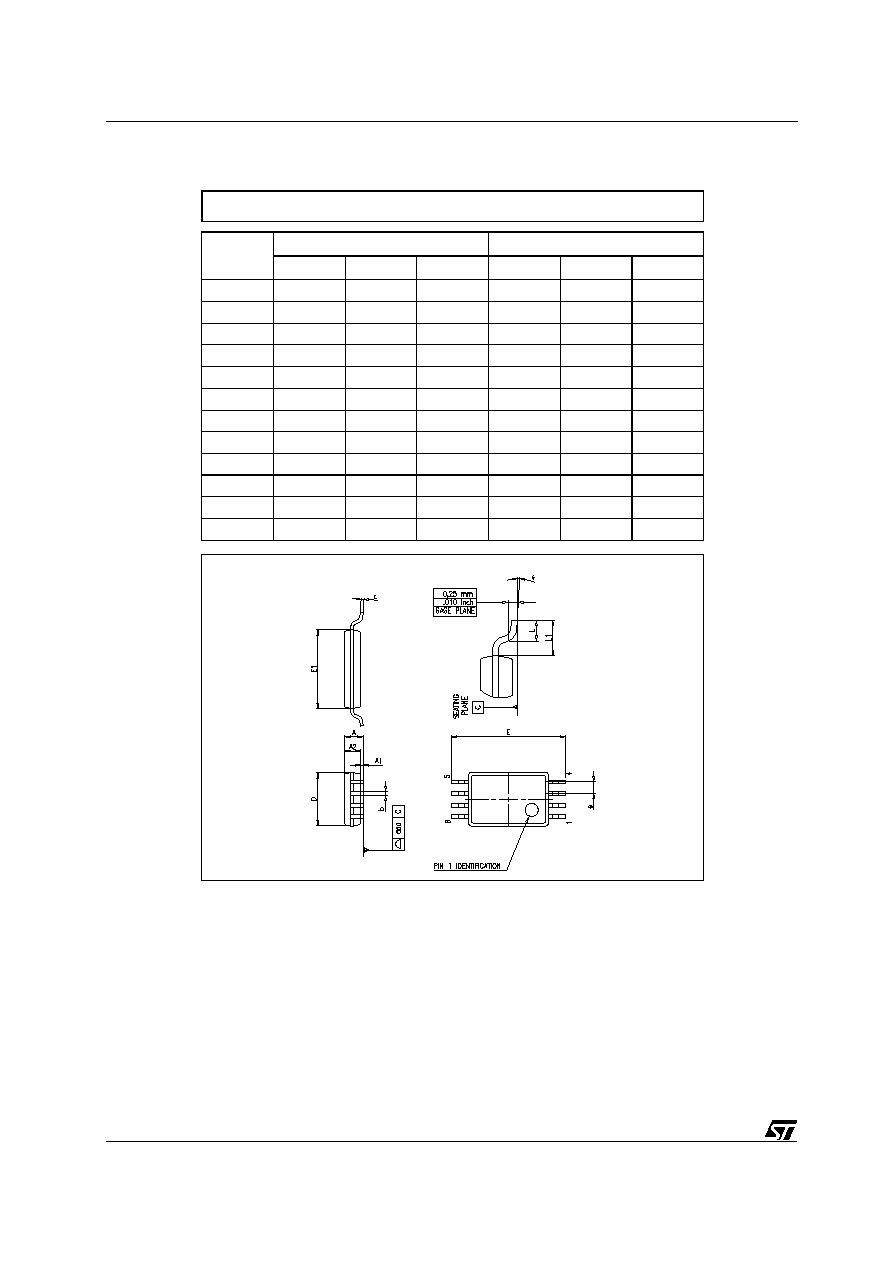
PACKAGE MECHANICAL DATA
DIM.
mm.
inch
MIN.
TYP
MAX.
MIN.
TYP.
MAX.
A
1.35
1.75
0.053
0.069
A1
0.10
0.25
0.04
0.010
A2
1.10
1.65
0.043
0.065
B
0.33
0.51
0.013
0.020
C
0.19
0.25
0.007
0.010
D
4.80
5.00
0.189
0.197
E
3.80
4.00
0.150
0.157
e
1.27
0.050
H
5.80
6.20
0.228
0.244
h
0.25
0.50
0.010
0.020
L
0.40
1.27
0.016
0.050
k
∞ (max.)
ddd
0.1
0.04
SO-8 MECHANICAL DATA
0016023/C
8
LM193W - LM293W - LM393W
10/10
Information furnished is believed to be accurate and reliable. However, STMicroelectronics assumes no responsibility for the
consequences of use of such information nor for any infringement of patents or other rights of third parties which may result from
its use. No license is granted by implication or otherwise under any patent or patent rights of STMicroelectronics. Specifications
mentioned in this publication are subject to change without notice. This publication supersedes and replaces all information
previously supplied. STMicroelectronics products are not authorized for use as critical components in life support devices or
systems without express written approval of STMicroelectronics.
The ST logo is a registered trademark of STMicroelectronics
All other names are the property of their respective owners
© 2004 STMicroelectronics - All Rights Reserved
STMicroelectronics GROUP OF COMPANIES
Australia - Belgium - Brazil - Canada - China - Czech Repubic - Finland - France - Germany - Hong Kong - India - Israel - Italy - Japan
Malaysia - Malta - Morocco - Singapore - Spain - Sweden - Switzerland - United Kingdom - United States
www.st.com
PACKAGE MECHANICAL DATA
DIM.
mm.
inch
MIN.
TYP
MAX.
MIN.
TYP.
MAX.
A
1.2
0.047
A1
0.05
0.15
0.002
0.006
A2
0.80
1.00
1.05
0.031
0.039
0.041
b
0.19
0.30
0.007
0.012
c
0.09
0.20
0.004
0.008
D
2.90
3.00
3.10
0.114
0.118
0.122
E
6.20
6.40
6.60
0.244
0.252
0.260
E1
4.30
4.40
4.50
0.169
0.173
0.177
e
0.65
0.0256
K
0∞
8∞
0∞
8∞
L
0.45
0.60
0.75
0.018
0.024
0.030
L1
1
0.039
TSSOP8 MECHANICAL DATA
0079397/D