LM138/238
LM338
March 1993
ADJUSTABLE VOLTAGE REGULATORS
THREE-TERMINAL 5-A
.
GUARANTEED 7A PEAK OUTPUT CURRENT
.
GUARANTEED 5A OUTPUT CURRENT
.
ADJUSTABLE OUTPUT DOWN TO 1.2V
.
LINE REGULATION TYPICALLY 0.005% /V
.
LOAD REGULATION TYPICALLY 0.1%
.
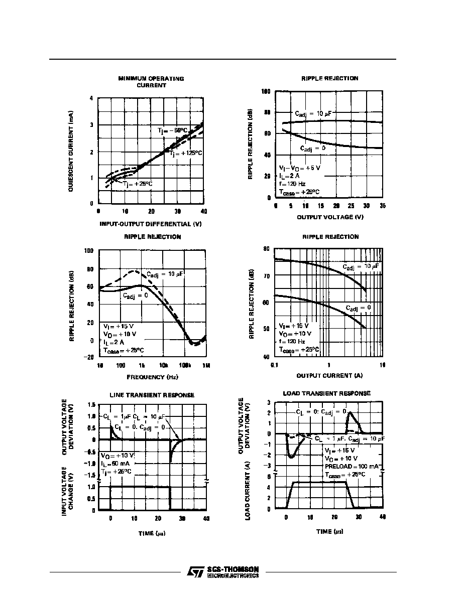
GUARANTEED THERMAL REGULATION
.
CURRENT LIMIT CONSTANT WITH TEM-
PERATURE
.
STANDARD 3-LEAD TRANSISTOR PACKAGE
DESCRIPTION
The LM138/LM238/LM338 are adjustable 3-terminal
positive voltage regulators capable of supplying in ex-
cess of 5A over a 1.2V to 32V output range. They are
exceptionally easy to use and require only 2 resistors
to set the output voltage. Careful circuit design has re-
sulted in outstanding load and line regulation com-
parable to many commercial power supplies. The
LM138 family is supplied in a standard 3-lead transis-
tor package.
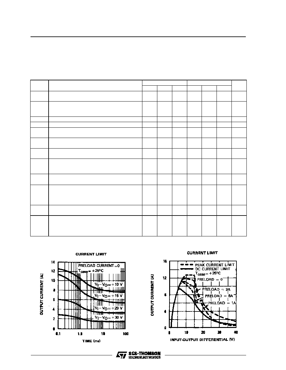
A unique feature of the LM138 family is time-de-
pendent current limiting. The current limit circuitry
allows peak currents of up to 12A to be drawn from the
regulator for short periods of time. This allows the
LM138 to be used with heavy transient loads and
speeds start-up under full-load conditions. Under sus-
tained loading conditions, the current limit decreases
to a safe value protecting the regulator. Also included
on the chip are thermal overload protection and safe
area protection for the power transistor. Overload pro-
tection remains functional even if the adjustment pin
is accidentally disconnected.
Normally, no capacitors are needed unless the device
is situated far from the input filter capacitors in which
case an input bypass is needed. An optional output
capacitor can be added to improve transient res-
ponse. The adjustment terminal can be bypassed to
achieve very high ripple rejection ratios which are dif-
ficult to achieve with standard 3-terminal regulators.
Besides replacing fixed regulators ordiscrete designs,
the LM238 is useful in a wide variety of other applica-
tions. Since the regulator is "floating" and sees only
theinput-to-output differential voltage, supplies of sev-
eral hundred volts can be regulated as long as the
maximum input to input differential is not exceeded.
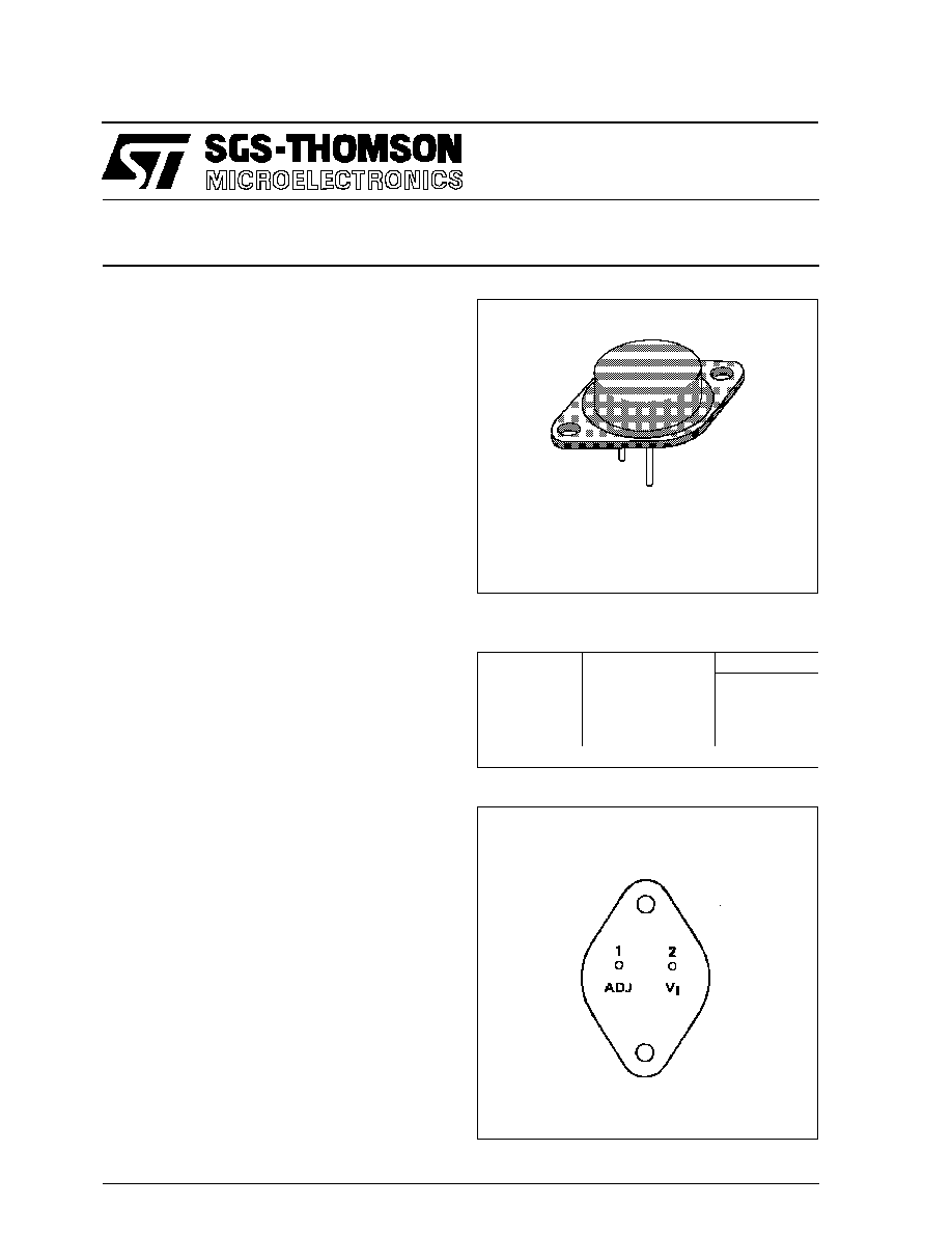
The LM138/LM238/LM338 are packaged in standard
steel TO-3 transistor packages. The LM138 is rated
for operation from -55
o
C to 150
o
C, the LM238 from
≠ 25
∞
C to + 150
∞
C and the LM338 from 0
∞
C to +
125
∞
C.
TO3
K SUFFIX
(Steel Can)
ORDER CODE
PART
NUMBER
TEMPERATURE
RANGE
PACKAGE
K
LM138
LM238
LM338
-55
o
C to + 150
o
C
-25
o
C to + 150
o
C
0
o
C to + 125
o
C
∑
∑
∑
EXAMPLE: LM138K
PIN CONNECTION
(bottom view)
Case is output
1/12
ABSOLUTE MAXIMUM RATING
Symbol
Parameter
Value
Unit
P
tot
Power Dissipation
Internally Limited
W
V
I
- V
O
Input-Output Voltage DIfferential
35
V
T
oper
Operating Junction Temperature Range
LM138
LM238
LM338
-55 to 150
-25 to 150
0 to 125
o
C
T
stg
Storage Temperature Range
-65 to 150
o
C
T
lead
Lead Temperature (Soldering, 10 seconds)
300
o
C
THERMAL CHARACTERISTICS
Symbol
Parameter
Value
Unit
R
th(j-c)
Typical Junction-Case Thermal Resistance
1.4
o
C/W
R
th(j-a)
Max Junction-Ambient Thermal Resistance
35
o
C/W
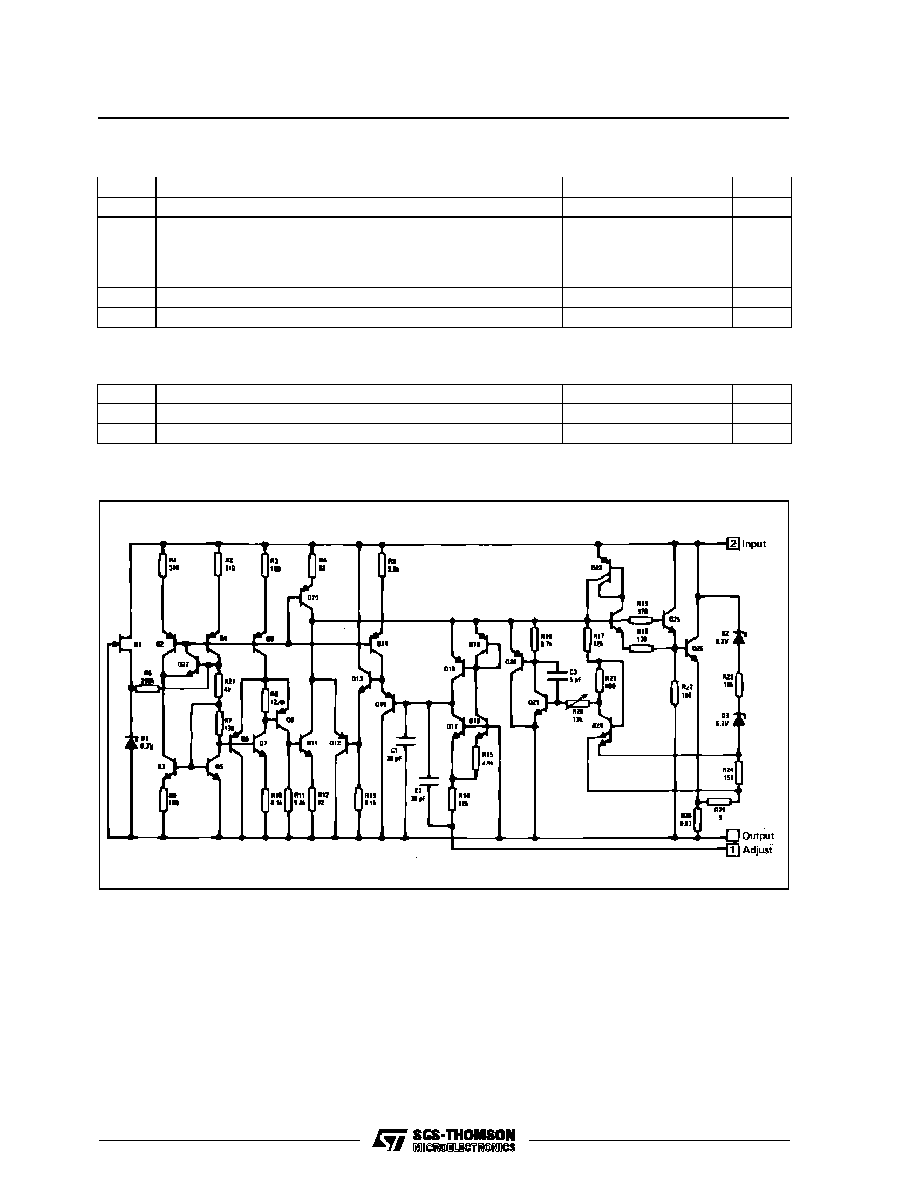
SCHEMATIC DIAGRAM
LM138-LM238-LM338
2/12
ELECTRICAL CHARACTERISTICS
LM138: -55
T
j
150
o
C, V
I
- V
O
= 5V, I
O
= 2.5A
LM238: -25
T
j
150
o
C, V
I
- V
O
= 5V, I
O
= 2.5A
LM338: 0
T
j
150
o
C, V
I
- V
O
= 5V, I
O
= 2.5A
Although power dissipation is internally limited, these specifications apply to power dissipation up to
50W (unless otherwise specified).
Symbol
Parameter
LM138-LM238
LM338
Unit
Min.
Typ.
Max.
Min.
Typ.
Max.
K
VI
Line Regulation - (note 1)
T
amb
= 25
o
C, 3 V
(V
I
- V
O
)
35 V
0.005
0.01
0.005
0.03
%/V
K
VO
Load Regulation T
amb
= 25
o
C, 10 mA
I
O
5 A
V
O
5V - (note 1)
V
O
5V - (note 1)
5
0.1
15
0.3
5
0.1
25
0.5
mV
%
Thermal Regulation (pulse = 20 ms)
0.002
0.01
0.002
0.02
%/W
I
adj
Adjustment Pin Current
45
100
45
100
µ
A
I
adj
Adjustment Pin Current Change
10 mA
I
L
5 A, 3 V
(V
I
- V
O
)
35 V
0.2
5
0.2
5
µ
A
v
(ref)
Reference Voltage
3V
(V
I
- V
O
)
35 V, 10 mA
I
O
5A, P
50W
1.19
1.24
1.29
1.19
1.24
1.29
V
K
VI
Line Regulation - (note 1)
3 V
(V
I
- V
O
)
35 V
0.02
0.04
0.02
0.06
%/V
K
VO
Load Regulation 10 mA
I
O
5 A
V
O
5V - (note 1)
V
O
5V - (note 1)
20
0.3
30
0.6
20
0.3
50
1
mV
%
K
VT
Temperature Stability (T
min
T
j
T
max
)
1
1
%
I
O(min)
Minimum Load Current (V
I
- V
O
35 V)
3.5
5
3.5
10
mA
I
O(max)
Current Limit (V
I
- V
O
10 V)
DC
0.5 ms Peak
V
I
- V
O
= 30 V
5
7
8
12
1
5
7
8
12
1
A
RMS Output Noise, % of V
O
(T
amb
= 25
o
C, 10 Hz
f
10 KHz)
0.003
0.003
%
R
vf
Ripple Rejection Ratio
V
O
= 10 V, f = 120 Hz
C
adi
= 10
µ
F
60
60
75
60
60
75
dB
K
VH
Long Term Stability (T
amb
= 125
o
C)
0.3
1
0.3
1
%
Note 1 : Regulation is measured at constant junction temperature. Changes in output voltage due to heating effects are taken
into account separately by thermal rejection.
LM138-LM238-LM338
3/12