 | –≠–ª–µ–∫—Ç—Ä–æ–Ω–Ω—ã–π –∫–æ–º–ø–æ–Ω–µ–Ω—Ç: LM2903HD | –°–∫–∞—á–∞—Ç—å:  PDF PDF  ZIP ZIP |
1/5
s
WIDE SINGLE SUPPLY VOLTAGE RANGE
OR DUAL SUPPLIES +2V TO +36V OR ±1V
TO ±18V
s
VERY LOW SUPPLY CURRENT (0.4mA)
INDEPENDENT OF SUPPLY VOLTAGE
(1mW/comparator at +5V)
s
LOW INPUT BIAS CURRENT: 25nA TYP
s
LOW INPUT OFFSET CURRENT: ±5nA TYP
s
INPUT COMMON-MODE VOLTAGE RANGE
INCLUDES GROUND
s
LOW OUTPUT SATURATION VOLTAGE:
250mV TYP. (I
O
= 4mA)
s
DIFFERENTIAL INPUT VOLTAGE RANGE
EQUAL TO THE SUPPLY VOLTAGE
s
TTL, DTL, ECL, MOS, CMOS COMPATIBLE
OUTPUTS
DESCRIPTION
This device consists of two independent low
power voltage comparators designed specifically
to operate from a single supply over a wide range
of voltages. Operation from split power supplies is
also possible.
These comparators also have a unique
characteristic in that the input common-mode
voltage range includes ground even though
operated from a single power supply voltage.
ORDER CODE
D = Small Outline Package (SO) - also available in Tape & Reel (DT)
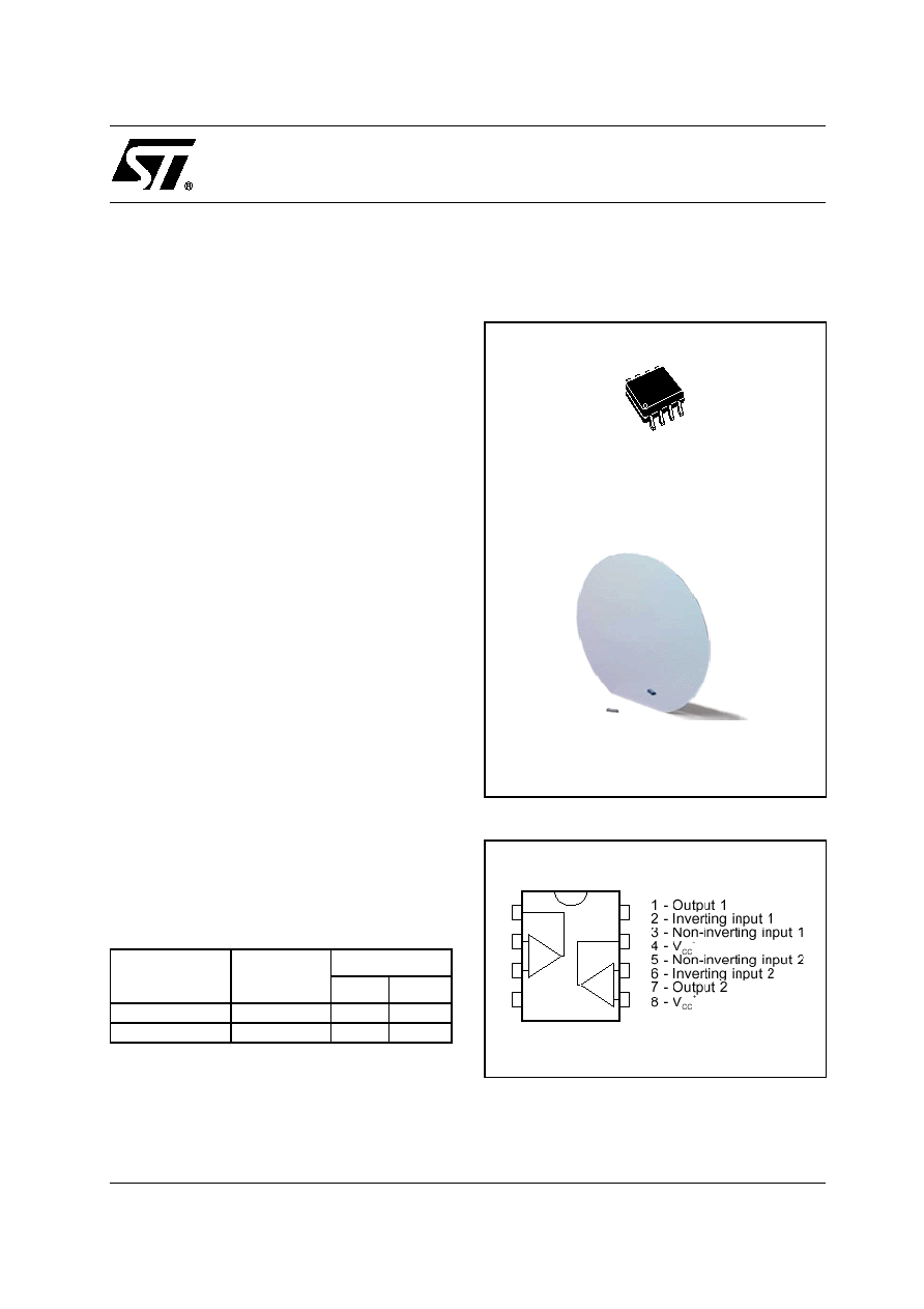
PIN CONNECTIONS (top view)
Part Number
Temperature
Range
Package
Wafer
SO8
JLM2903H- E6D1
-40∞C, +150∞C
∑
LM2903HD
-40∞C, +150∞C
∑
D
SO-8
(Plastic Micropackage)
Wafer form
1
2
3
4
5
6
7
8
-
+
-
+
LM2903H
LOW POWER DUAL VOLTAGE COMPARATORS
.
September 2003
LM2903H
2/5
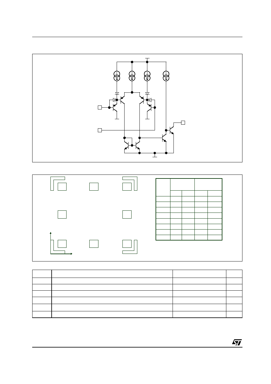
SCHEMATIC DIAGRAM (1/2 LM2903)
PAD LOCATIONS
ABSOLUTE MAXIMUM RATINGS
VCC-
VCC-
VCC+
VCC-
3.5µA
100µA
3.5µA
100µA
Vo
Non-Inverting
Inverting
Input
Input
Symbol
Parameter
Value
Unit
V
CC
Supply Voltage
±18 or 36
V
V
ID
Differential Input Voltage
±36
V
V
I
Input Voltage
-0.3 to +36
V
Output Short-circuit to Ground
1)
1.
Short-circuit from the output to V
cc
+
can cause excessive heating and eventual destruction. The maximum output current is approximately 20mA,
independent of the magnitude of V
cc
+
20
mA
P
d
Power Dissipation at T
AMB
=+25∞C
2)
2.
Pd is calculated with T
amb
= +25∞C, T
Junction
= +150∞C and R
thja
= 175∞C/W for SO8 package
710
mW
T
stg
Storage Temperature Range
-65 to +150
∞C
OUT 1
OUT 2
Vcc +
E- (1)
E+ (1)
E- (2)
GND
E+ (2)
year
Die id.
x
y
90
90
730
90
OUT2
90
90
415
65
Vcc +
90
90
100
100
OUT1
90
90
100
400
E-1
90
90
100
750
E+1
90
90
415
830
GND
Pad dimensions
Pad placement
Name
90
90
720
760
E+2
90
90
720
410
E-2
Y
X
Y
X
90
90
730
90
OUT2
90
90
415
65
Vcc +
90
90
100
100
OUT1
90
90
100
400
E-1
90
90
100
750
E+1
90
90
415
830
GND
Pad dimensions
Pad placement
Name
90
90
720
760
E+2
90
90
720
410
E-2
Y
X
Y
X
All dimensions are specified in micrometer (um).
LM2903H
3/5
OPERATING CONDITIONS
ELECTRICAL CHARACTERISTICS
V
CC
+
= 5V, V
cc
-
= GND, T
amb
= 25∞C (unless otherwise specified)
Symbol
Parameter
Value
Unit
V
CC
+
Supply Voltage
2 to 36
V
T
oper
Operating Free-Air Temperature Range
-40 to +150
∞C
Symbol
Parameter
Min.
Typ.
Max.
Unit
V
IO
Input Offset Voltage
1)
T
amb
= +25∞C
T
min
T
amb
T
max
.
1.
At output switch point, V
O
1.4V, R
S
= 0
with V
CC
+
from 5V to 30V, and over the full input common-mode range (0V to V
CC
+
≠1.5V).
1
7
15
mV
I
IO
Input Offset Current
T
amb
= +25∞C
T
min
T
amb
T
max.
5
50
150
nA
I
IB
Input Bias Current
2)
T
amb
= +25∞C
T
min
T
amb
T
max.
2.
The direction of the input current is out of the IC due to the PNP input stage. This current is essentially constant, independent of the state of the
output, so no loading charge exists on the reference of input lines
25
250
400
nA
A
VD
Large Signal Voltage Gain (V
cc
= 15V,R
L
=15k
, V
o
=1 to 11V)
25
200
V/mV
I
CC
Supply Current (all comparators)
V
CC
= 5V, no load
V
CC
= 30V, no load
0.4
1
1
2.5
mA
V
ICM
Input Common Mode Voltage Range (V
cc
= 30V)
3)
T
amb
= +25∞C
T
min
T
amb
T
max.
3.
The input common-mode voltage of either input signal voltage should not be allowed to go negative by more than 0.3V. The upper end of the
common-mode voltage range is V
CC
+
≠1.5V, but either or both inputs can go to +30V without damage.
0
0
V
CC
+
-1.5
V
CC
+
-2
V
V
ID
Differential Input Voltage
4)
4.
Positive excursions of input voltage may exceed the power supply level. As long as the other voltage remains within the common-mode range, the
comparator will provide a proper output state.
The low input voltage state must not be less than ≠0.3V (or 0.3V below the negative power supply, if used)
V
CC
+
V
V
OL
Low Level Output Voltage (V
id
= -1V, I
sink
= 4mA)
T
amb
= +25∞C
T
min
T
amb
T
max
250
400
800
mV
I
OH
High Level Output Current (V
CC
=V
o
=30V, V
id
= 1V)
T
amb
= +25∞C
T
min
T
amb
T
max
0.1
1
nA
µ
A
I
SINK
Output Sink Current (V
id
= -1V,V
o
= 1.5V)
T
amb
= +25∞C
T
min
T
amb
T
max
6
2
16
m
t
RE
Small Signal Response Time
5)
(R
L
= 5.1k
to V
CC
+
)
5.
The response time specified is for a 100mV input step with 5mV overdrive.
1.3
µ
s
t
REL
Large Signal Response Time
6)
TTL Input (V
ref
= +1.4 V, R
L
=5.1k
to V
CC
+
)
Output Signal at 50% of final value
Output Signal at 95% of final value
6.
Maximum values are guaranteed by design & evaluation.
500
1
ns
µ
s
LM2903H
4/5
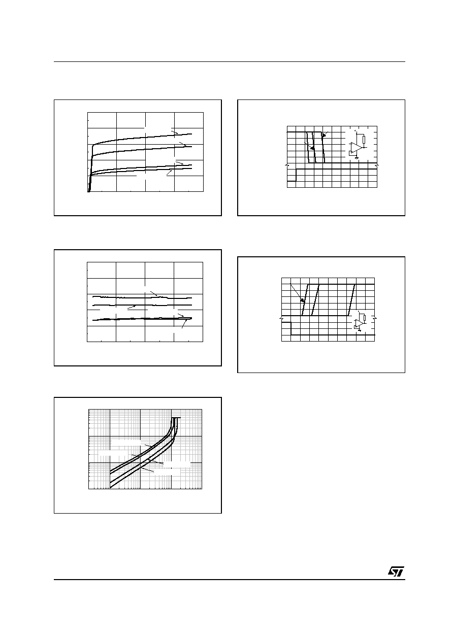
SUPPLY CURRENT versus SUPPLY VOLTAGE
INPUT CURRENT versus SUPPLY VOLTAGE
OUTPUT SATURATION VOLTAGE versus
OUTPUT CURRENT (Vcc=5V)
RESPONSE TIME FOR VARIOUS INPUT
OVERDRIVES - NEGATIVE TRANSITION
RESPONSE TIME FOR VARIOUS INPUT
OVERDRIVES - POSITIVE TRANSITION
0
10
20
30
40
0.0
0.2
0.4
0.6
0.8
1.0
T
AM B
= + 150 ∞C
T
AMB
= + 125 ∞C
T
AMB
= + 25 ∞C
T
AMB
= - 40 ∞C
S
U
P
P
L
Y
CURR
E
N
T
(
m
A)
SUPPLY VOLTAGE (V)
0
10
20
30
40
0
10
20
30
40
50
T
AMB
= + 150 ∞C
T
AMB
= + 125 ∞C
T
AMB
= + 25 ∞C
T
AMB
= - 40 ∞C
I
N
P
U
T
B
I
AS
CUR
RE
NT
(
n
A)
SUPPLY VOLTAGE (V)
0.1
1
10
100
0.01
0.1
1
10
T
AMB
= - 40 ∞C
T
AMB
= + 25 ∞C
T
AMB
= + 125 ∞C
T
AMB
= + 150 ∞C
OU
TP
U
T
S
A
TU
R
A
T
I
O
N
V
O
LT
A
G
E
(
V
)
OUTPUT SINK CURRENT (mA)
5V
5.1k
W
e
o
e
I
6
5
4
3
2
1
0
0
-50
-100
INPUT VOLTAGE (mV) OUTPUT VOLTAGE (V)
0
0.5
1
1.5
2
TIME (
m
s)
Input overdrive : 5mV
20mV
100mV
T
amb
= +25∞C
5V
5.1k
W
e
o
e
I
6
5
4
3
2
1
0
100
50
INPUT VOLTAGE (mV) OUTPUT VOLTAGE (V)
0
0.5
1
1.5
2
TIME (
m
s)
Input overdrive : 100mV
20mV
5mV
T
amb
= +25∞C
0
LM2903H
5/5
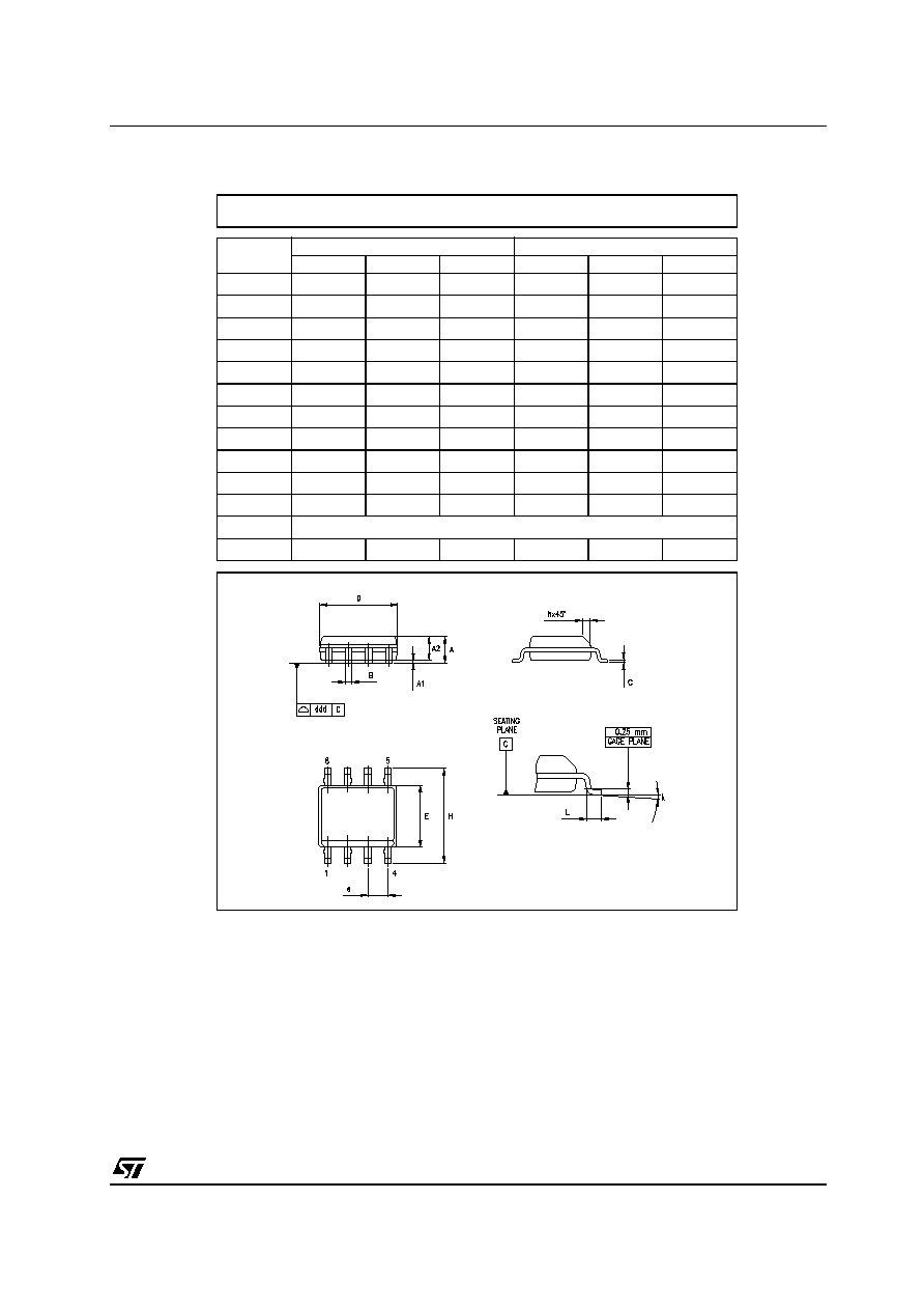
PACKAGE MECHANICAL DATA
DIM.
mm.
inch
MIN.
TYP
MAX.
MIN.
TYP.
MAX.
A
1.35
1.75
0.053
0.069
A1
0.10
0.25
0.04
0.010
A2
1.10
1.65
0.043
0.065
B
0.33
0.51
0.013
0.020
C
0.19
0.25
0.007
0.010
D
4.80
5.00
0.189
0.197
E
3.80
4.00
0.150
0.157
e
1.27
0.050
H
5.80
6.20
0.228
0.244
h
0.25
0.50
0.010
0.020
L
0.40
1.27
0.016
0.050
k
∞ (max.)
ddd
0.1
0.04
SO-8 MECHANICAL DATA
0016023/C
8
Information furnished is believed to be accurate and reliable. However, STMicroelectronics assumes no responsibility for the
consequences of use of such information nor for any infringement of patents or other rights of third parties which may result from
its use. No license is granted by implication or otherwise under any patent or patent rights of STMicroelectronics. Specifications
mentioned in this publication are subject to change without notice. This publication supersedes and replaces all information
previously supplied. STMicroelectronics products are not authorized for use as critical components in life support devices or
systems without express written approval of STMicroelectronics.
The ST logo is a registered trademark of STMicroelectronics
All other names are the property of their respective owners.
© 2003 STMicroelectronics - All Rights Reserved
STMicroelectronics GROUP OF COMPANIES
Australia - Belgium - Brazil - Canada - China - Czech Repubic - Finland - France - Germany
Hong Kong - India - Israel - Italy - Japan - Malaysia - Malta - Morocco - Singapore - Spain
Sweden - Switzerland - United Kingdom - United States
http://www.st.com