 | –≠–ª–µ–∫—Ç—Ä–æ–Ω–Ω—ã–π –∫–æ–º–ø–æ–Ω–µ–Ω—Ç: LM358AWDT | –°–∫–∞—á–∞—Ç—å:  PDF PDF  ZIP ZIP |
Rev 2
July 2005
1/16
16
LM358W-LM358AW
Low Power Dual Operational Amplifiers
Internally frequency compensated
Large DC voltage gain: 100dB
Wide bandwidth (unity gain): 1.1mHz
(temperature compensated)
Very low supply current/op (500µA) essentially
independent of supply voltage
Low input bias current: 20nA
(temperature compensated)
Low input offset voltage: 2mV
Low input offset current: 2nA
Input common-mode voltage range includes
ground
Differential input voltage range equal to the
power supply voltage
Large output voltage swing 0V to (Vcc - 1.5V)
ESD internal protection: 1.5kV
Description
These circuits consist of two independent, high-
gain, internally frequency-compensated which
were designed specifically to operate from a
single power supply over a wide range of voltages.
The low power supply drain is independent of the
magnitude of the power supply voltage.
Application areas include transducer amplifiers,
DC gain blocks and all the conventional op-amp
circuits which now can be more easily
implemented in single power supply systems. For
example, these circuits can be directly supplied
with the standard +5V which is used in logic
systems and will easily provide the required
interface electronics without requiring any
additional power supply.
In the linear mode the input common-mode
voltage range includes ground and the output
voltage can also swing to ground, even though
operated from only a single power supply voltage.
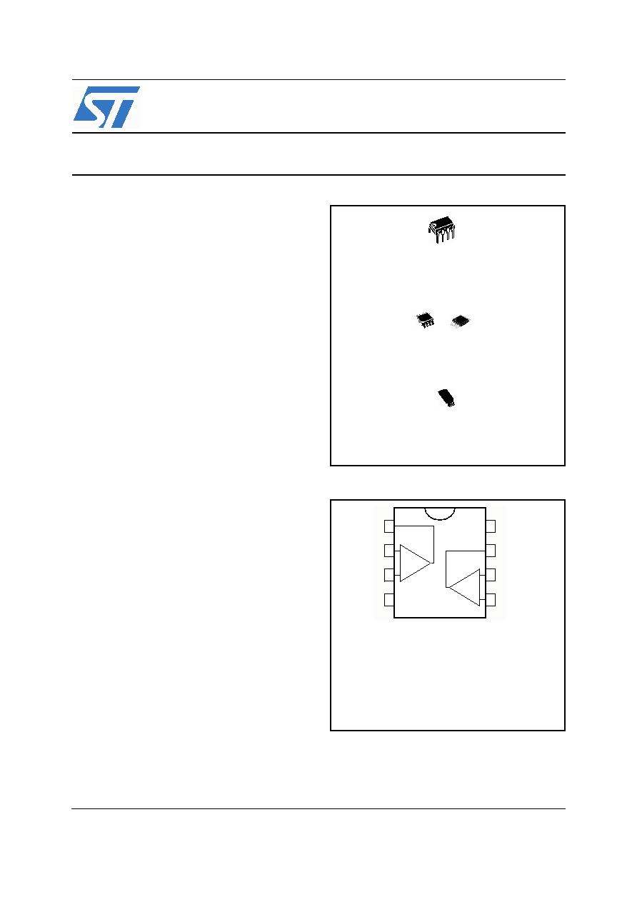
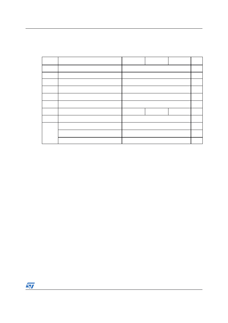
Pin Connections (top view)
N
DIP-8
(Plastic Package)
D & S
SO-8 & miniSO-8
(Plastic Micropackage)
P
TSSOP8
(Thin Shrink Small Outline Package)
1 - Output 1
2 - Inverting input
3 - Non-inverting input
4 - V
CC
-
5 - Non-inverting input 2
6 - Inverting input 2
7 - Output 2
8 - V
CC
+
1
2
3
4
5
6
7
8
-
+
-
+
www.st.com

LM358W-LM358AW
2/16
Order Codes
Part Number
Temperature
Range
Package
Packaging
Marking
LM358WN
0∞C, +70∞C
DIP-8
Tube
LM358WN
LM358WD
LM358WDT
SO-8
Tube or Tape & Reel
358W
LM358AWD
LM358AWDT
358AW
LM358W-LM358AW
Absolute Maximum Ratings
3/16
1
Absolute Maximum Ratings
Table 1.
Key parameters and their absolute maximum ratings
Symbol
Parameter
LM158W,AW LM258W,AW LM358W,AW
Unit
V
CC
Supply voltage
+32
V
Vi
Input Voltage
-0.3 to +32
V
V
id
Differential Input Voltage
+32
V
P
tot
Power Dissipation
(1)
1.
Power dissipation must be considered to ensure maximum junction temperature (Tj) is not exceeded.
500
mW
Output Short-circuit Duration
(2)
2.
Short-circuits from the output to V
CC
can cause excessive heating if V
CC
> 15V. The maximum output current is
approximately 40mA independent of the magnitude of V
CC
. Destructive dissipation can result from
simultaneous short-circuit on all amplifiers.
Infinite
I
in
Input Current
(3)
3.
This input current only exists when the voltage at any of the input leads is driven negative. It is due to the
collector-base junction of the input PNP transistor becoming forward biased and thereby acting as input diodes
clamps. In addition to this diode action, there is also NPN parasitic action on the IC chip. this transistor action
can cause the output voltages of the Op-amps to go to the V
CC
voltage level (or to ground for a large overdrive)
for the time duration than an input is driven negative. This is not destructive and normal output will set up again
for input voltage higher than -0.3V.
50
mA
T
oper
Operating Free-air Temperature Range
-55 to +125
-40 to +105
0 to +70
∞C
T
stg
Storage Temperature Range
-65 to +150
∞C
ESD
HBM: Human Body Model
(4)
4.
Human body model, 100pF discharged through a 1.5k
resistor into pin of device.
1.5
kV
MM: Machine Model
(5)
5.
Machine model ESD, a 200pF cap is charged to the specified voltage, then discharged directly into the IC with
no external series resistor (internal resistor < 5
), into pin to pin of device.
200
V
CDM: Charged Device Model
1.5
kV
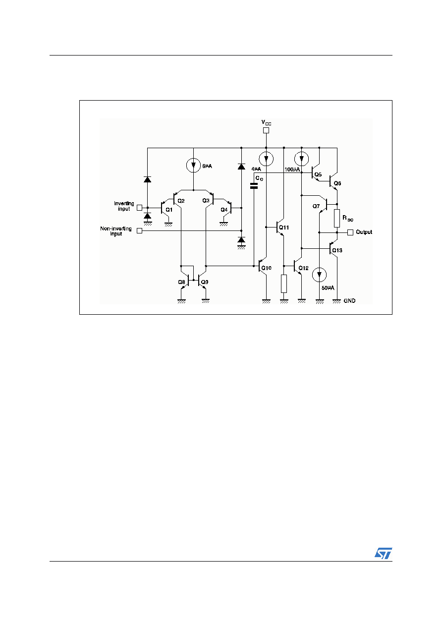
Typical Application Schematic
LM358W-LM358AW
4/16
2 Typical
Application
Schematic
Figure 1.
Schematic diagram (1/2 LM158W)
LM358W-LM358AW
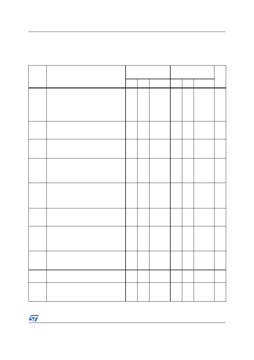
Electrical Characteristics
5/16
3 Electrical
Characteristics
Table 2.
V
CC
+
= +5V, V
CC
-
= Ground, V
o
= 1.4V, T
amb
= +25∞C (unless otherwise specified)
Symbol
Parameter
LM158AW-LM258AW
LM358AW
LM158W-LM258W
LM358W
Unit
Min.
Typ.
Max.
Min.
Typ.
Max.
V
io
Input Offset Voltage - note
(1)
T
amb
= +25∞C
LM158, LM258
LM158A
T
min
T
amb
T
max
LM158, LM258
1
3
2
4
2
7
5
9
7
mV
I
io
Input Offset Current
T
amb
= +25∞C
T
min
T
amb
T
max
2
10
30
2
30
40
nA
I
ib
Input Bias Current - note
(2)
T
amb
= +25∞C
T
min
T
amb
T
max
20
50
100
20
150
200
nA
A
vd
Large Signal Voltage Gain
V
CC
= +15V, R
L
= 2k
, V
o
= 1.4V to 11.4V
T
amb
= +25∞C
T
min
T
amb
T
max
50
25
100
50
25
100
V/
mV
SVR
Supply Voltage Rejection Ratio (R
s
10k)
V
CC
+
= 5V to 30V
T
amb
= +25∞C
T
min
T
amb
T
max
65
65
100
65
65
100
dB
I
CC
Supply Current, all Amp, no load
T
min
T
amb
T
max
, V
CC
= +5V
T
min
T
amb
T
max
, V
CC
= +30V
0.7
1.2
1
0.7
1.2
2
mA
V
icm
Input Common Mode Voltage Range
V
CC
= +30V - note
(3)
T
amb
= +25∞C
T
min
T
amb
T
max
0
0
V
CC
+
-1.5
V
CC
+
-2
0
0
V
CC
+
-1.5
V
CC
+
-2
V
CMR
Common Mode Rejection Ratio (R
s
10k)
T
amb
= +25∞C
T
min
T
amb
T
max
70
60
85
70
60
85
dB
I
source
Output Current Source
V
CC
= +15V, V
o
= +2V, V
id
= +1V
20
40
60
20
40
60
mA
I
sink
Output Sink Current (V
id
= -1V)
V
CC
= +15V, V
o
= +2V
V
CC
= +15V, V
o
= +0.2V
10
12
20
50
10
12
20
50
mA
µA
Electrical Characteristics
LM358W-LM358AW
6/16
V
OPP
Output Voltage Swing ( R
L
= 2k
)
T
amb
= +25∞C
T
min
T
amb
T
max
0
0
V
CC
+
-1.5
V
CC
+
-2
0
0
V
CC
+
-1.5
V
CC
+
-2
V
OH
High Level Output Voltage (V
CC
+
= 30V)
T
amb
= +25∞C, R
L
= 2k
T
min
T
amb
T
max
T
amb
= +25∞C, R
L
= 10k
T
min
T
amb
T
max
26
26
27
27
27
28
26
26
27
27
27
28
V
V
OL
Low Level Output Voltage (R
L
= 10k
)
T
amb
= +25∞C
T
min
T
amb
T
max
5
20
20
5
20
20
mV
SR
Slew Rate
V
CC
= 15V, V
i
= 0.5 to 3V, R
L
= 2k
,
C
L
= 100pF, unity Gain
0.3
0.6
0.3
0.6
V/
µs
GBP
Gain Bandwidth Product
V
CC
= 30V, f =100kHz,V
in
= 10mV, R
L
= 2k
,
C
L
= 100pF
0.7
1.1
0.7
1.1
MHz
THD
Total Harmonic Distortion
f = 1kHz, A
v
= 20dB, R
L
= 2k
, V
o
= 2V
pp
,
C
L
= 100pF, V
O
= 2Vpp
0.02
0.02
%
e
n
Equivalent Input Noise Voltage
f = 1kHz, R
s
= 100
, V
CC
= 30V
55
55
DV
io
Input Offset Voltage Drift
7
15
7
30
µV/
∞C
DI
Iio
Input Offset Current Drift
10
200
10
300
pA/
∞C
V
o1
/V
o2
Channel Separation - note
(4)
1kHz
f 20kHZ
120
120
dB
1.
V
o
= 1.4V, R
s
= 0
, 5V < V
CC
+
< 30V, 0 < V
ic
< V
CC
+
- 1.5V
2.
The direction of the input current is out of the IC. This current is essentially constant, independent of the state of the output
so no loading change exists on the input lines.
3.
The input common-mode voltage of either input signal voltage should not be allowed to go negative by more than 0.3V. The
upper end of the common-mode voltage range is V
CC
+
- 1.5V, but either or both inputs can go to +32V without damage.
4.
Due to the proximity of external components insure that coupling is not originating via stray capacitance between these
external parts. This typically can be detected as this type of capacitance increases at higher frequences.
Table 2.
V
CC
+
= +5V, V
CC
-
= Ground, V
o
= 1.4V, T
amb
= +25∞C (unless otherwise specified)
Symbol
Parameter
LM158AW-LM258AW
LM358AW
LM158W-LM258W
LM358W
Unit
Min.
Typ.
Max.
Min.
Typ.
Max.
nV
Hz
------------
LM358W-LM358AW
Electrical Characteristics
7/16
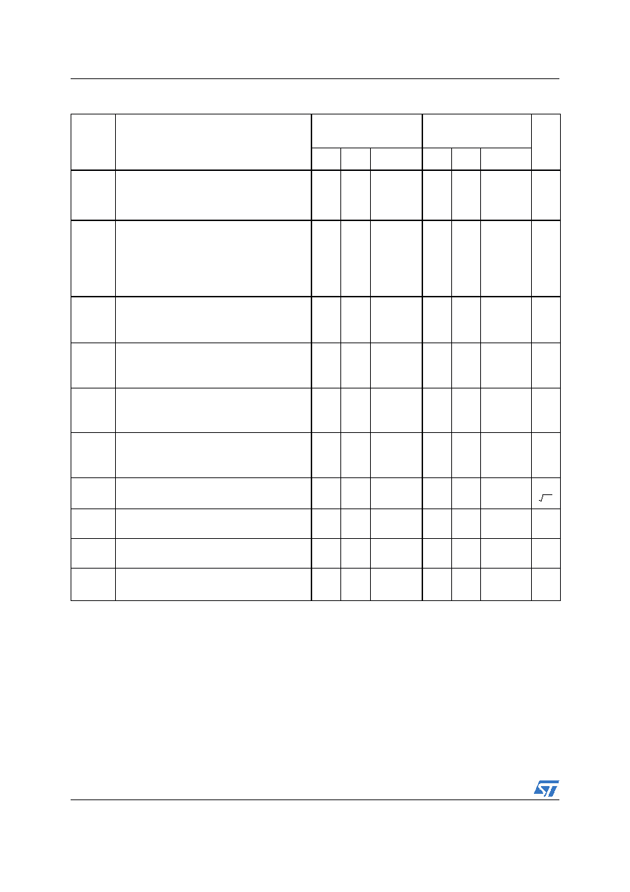
Figure 2.
Open loop frequency response
Figure 3.
Large signal frequency response
Figure 4.
Voltage follower pulse response
Figure 5.
Voltage follower pulse response
Figure 6.
Input current
Figure 7.
Output characteristics
VOLTAGE GAIN (dB)
OPEN LOOP FREQUENCY RESPONSE
(NOTE 3)
1.0
10 100 1k
10k 100k 1M 10M
VCC = +10 to + 15V &
FREQUENCY (Hz)
10M W
VI
VCC/2
VCC = 30V &
0.1mF
VCC
VO
-
+
-55∞C Tamb +125∞C
140
120
100
80
60
40
20
0
-55∞C Tamb +125∞C
LARGE SIGNAL FREQUENCY RESPONSE
FREQUENCY (Hz)
1k 10k 100k 1M
OUT
P
UT SWING (
V
pp)
+7V
2k W
1k W
100k W
+15V
VO
-
+
VI
20
15
10
5
0
INPUT
VOLTAGE (V)
OUTPUT
VOLTAGE (V)
VOLAGE FOLLOWER PULSE RESPONSE
0
10
20
30
40
TIME (ms)
RL 2 kW
VCC = +15V
4
3
2
1
0
3
2
1
OUT
P
UT
V
OLTAGE (m
V
)
VOLTAGE FOLLOWER PULSSE RESPONSE
(SMALL SIGNAL)
0 1 2 3 4 5 6 7 8
Input
Tamb = +25∞C
VCC = 30 V
Output
eO
el
50pF
+
-
TIME (ms)
500
450
400
350
300
250
IN
P
UT CURRENT (mA)
INPUT CURRENT (Note 1)
-55 -35 -15
5
25
45 65
85 105 125
VI = 0 V
VCC = +30 V
VCC = +15 V
VCC = +5 V
TEMPERATURE (∞C)
90
80
70
60
50
40
30
20
10
0
OUTPUT CHARACTERISTICS
OUTPUT SINK CURRENT (mA)
0,001 0,01 0,1 1 10 100
OUT
P
UT VOLTAGE (V)
VCC = +5V
VCC = +15V
VCC = +30V
-
IO
VO
Tamb = +25∞C
vcc/2
vcc
+
10
1
0.1
0.01
Electrical Characteristics
LM358W-LM358AW
8/16
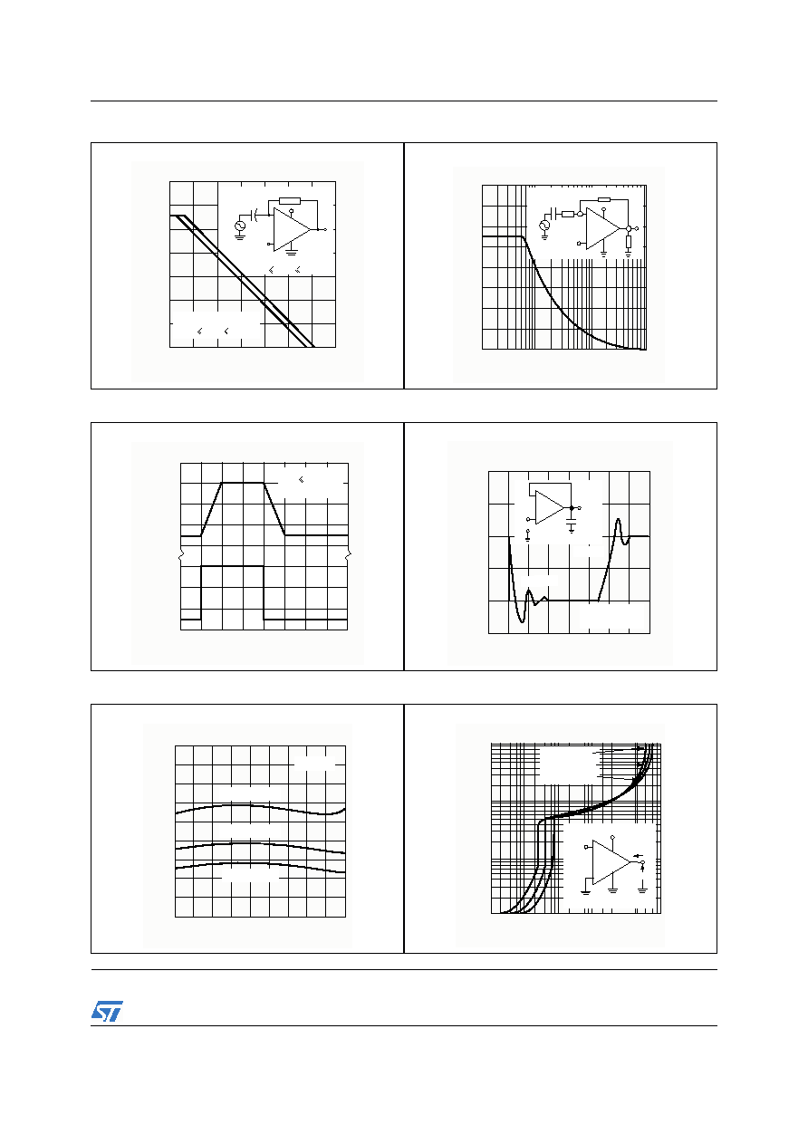
Figure 8.
Output characteristics
Figure 9.
Current limiting
Figure 10. Input voltage range
Figure 11. Positive supply voltage
Figure 12. Input voltage range
Figure 13. Supply current
OUT
P
UT
V
OLTAGE REFERENCED
TO
V CC
+ (
V
)
OUTPUT CHARACTERISTICS
0,01
0,1
1
10 100
0,001
Independent of VCC
Tamb = +25∞C
+
-
VCC
VO
IO
VCC /2
OUTPUT SOURCE CURRENT (mA)
8
7
6
5
4
3
2
1
OUT
P
UT CURRENT (mA)
CURRENT LIMITING (Note 1)
-
+
IO
TEMPERATURE (∞C)
90
80
70
60
50
40
30
20
10
0
-55 -35 -15
5
25
45 65
85 105 125
IN
P
UT
V
OLTAGE (
V
)
INPUT VOLTAGE RANGE
0
5
10
15
POWER SUPPLY VOLTAGE (±V)
NÈgative
Positive
15
10
5
0 10 20 30 40
POSITIVE SUPPLY VOLTAGE (V)
V
OL
TA
GE
GAIN (
d
B)
160
120
80
40
L
R = 20k W
L
R = 2k W
0 10 20 30
POSITIVE SUPPLY VOLTAGE (V)
VOLTAGE GAIN (dB)
160
120
80
40
L
R = 20k W
L
R = 2k W
SU
PP
LY CURRENT (mA)
SUPPLY CURRENT
0
10
20
30
Tamb = -55∞C
VCC
mA
ID
-
+
Tamb = 0∞C to +125∞C
POSITIVE SUPPLY VOLTAGE (V)
4
3
2
1
LM358W-LM358AW
Electrical Characteristics
9/16
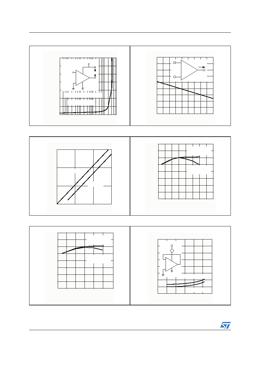
Figure 14. Input current
Figure 15. Gain bandwidth product
Figure 16. Power supply rejection ratio
Figure 17. Common mode rejection ratio
0 10 20 30
POSITIVE SUPPLY VOLTAGE (V)
IN
P
UT CURRENT (nA)
100
75
50
25
amb
T = +25∞C
-55-35-15 5 25 45 65 85 105 125
TEMPERATURE (∞C)
GAIN
B
AN
D
WI
D
TH
P
RO
D
UCT (MH
z
)
CC
V = 15V
1.5
1.35
1.2
1.05
0.9
0.75
0.6
0.45
0.3
0.15
0
-55-35-15 5 25 45 65 85 105 125
TEMPERATURE (∞C)
POWER SUPPLY REJECTION RATIO (
dB
)
SVR
115
110
105
100
95
90
85
80
75
70
65
60
-55-35-15 5 25 45 65 85 105 125
TEMPERATURE (∞C)
COMMON MO
D
E RE
J
ECTION RATIO (
dB
)
115
110
105
100
95
90
85
80
75
70
65
60
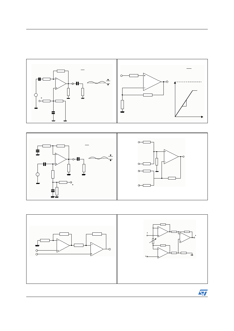
Typical Applications
LM358W-LM358AW
10/16
4 Typical
Applications
(single supply voltage) V
cc
= +5V
dc
Figure 18. AC coupled inverting amplifier
Figure 19. Non-inverting DC amplifier
Figure 20. AC coupled non-inverting amplifier
Figure 21. DC summing amplifier
Figure 22. High input Z, DC differential amplifier Figure 23. High input Z adjustable gain DC
instrumentation amplifier
1/2
LM158
~
0
2V
PP
R
10k
W
L
C
o
e
o
R
6.2k
W
B
R
100k
W
f
R1
10k
W
C
I
e
I
V
CC
R2
100k
W
C1
10mF
R3
100k
W
A = -
R
R1
V
f
(as shown A
= -10)
V
R1
10k
W
R2
1M
W
1/2
LM158
10k
W
e
I
e
O
+5V
e
O
(V
)
(mV)
0
A
V
= 1 +
R2
R1
(As shown
= 101)
A
V
1/2
LM158
~
0
2V
PP
R
10k
W
L
C
o
e
o
R
6.2k
W
B
C1
0.1
mF
e
I
V
CC
(as shown A
= 11)
V
A = 1 + R2
R1
V
R1
100k
W
R2
1M
W
C
I
R3
1M
W
R4
100k
W
R5
100k
W
C2
10mF
1/2
LM158
e
O
e
4
e
3
e
2
e
1
100k
W
100k
W
100k
W
100k
W
100k
W
100k
W
e
o
= e
1
+ e
2
- e
3
- e
4
where (e1 + e
2
)
(e
3
+ e
4
)
to keep e
o
0V
R1
100k
W
R2
100k
W
R4
100k
W
R3
100k
W
+V2
+V1
V
o
1/2
LM158
1/2
LM158
if R1 = R5 and R3 = R4 = R6 = R7
e
o
= [1 + ] ( (e
2
+ e
1
)
As shown e
o
= 101 (e
2
+ e
1
)
2R1
R2
-----------
R3
100k
W
e
O
1/2
LM158
R1
100k
W
e
1
R7
100k
W
R6
100k
W
R5
100k
W
e
2
R2
2k
W
Gain adjust
R4
100k
W
1/2
LM158
1/2
LM158
if R1 = R5 and
R3 = R4 = R6 = R7
e
o
= [ 1 + ] ( (e
2
+ e
1
)
As shown e
o
= 101 (e
2
+ e
1
)
2R1
R2
-----------
LM358W-LM358AW
Typical Applications
11/16
Figure 24. Using symmetrical amplifiers to
reduce input current
Figure 25. Low drift peak detector
Figure 26. Active band-pass filter
1/2
LM158
I
B
2N 929
0.001mF
I
B
3M
W
I
B
e
o
I
I
e
I
I
B
I
B
Input current compensation
1.5M
W
1/2
LM158
I
B
2N 929
0.001
mF
I
B
3R
3M
W
I
B
Input current
compensation
e
o
I
B
e
I
1/2
LM158
Z
o
Z
I
C
1
mF
2I
B
R
1M
W
2I
B
1/2
LM158
1/2
LM158
1/2
LM158
R8
100k
W
C3
10
mF
R7
100k
W
R5
470k
W
C1
330pF
V
o
V
CC
R6
470k
W
C2
330pF
R4
10M
W
R1
100k
W
R2
100k
W
+V1
R3
100k
W
1/2
LM158
1/2
LM158
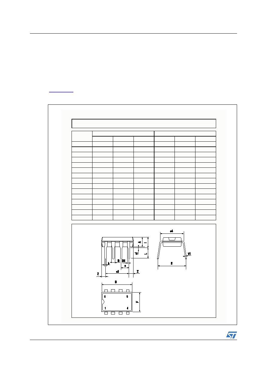
Package Mechanical Data
LM358W-LM358AW
12/16
5
Package Mechanical Data
In order to meet environmental requirements, ST offers these devices in ECOPACK
Æ
packages.
These packages have a Lead-free second level interconnect. The category of second level
interconnect is marked on the package and on the inner box label, in compliance with JEDEC
Standard JESD97. The maximum ratings related to soldering conditions are also marked on
the inner box label. ECOPACK is an ST trademark. ECOPACK specifications are available at:
www.st.com
..
5.1 DIP8
Package
DIM.
mm.
inch
MIN.
TYP
MAX.
MIN.
TYP.
MAX.
A
3.3
0.130
a1
0.7
0.028
B
1.39
1.65
0.055
0.065
B1
0.91
1.04
0.036
0.041
b
0.5
0.020
b1
0.38
0.5
0.015
0.020
D
9.8
0.386
E
8.8
0.346
e
2.54
0.100
e3
7.62
0.300
e4
7.62
0.300
F
7.1
0.280
I
4.8
0.189
L
3.3
0.130
Z
0.44
1.6
0.017
0.063
Plastic DIP-8 MECHANICAL DATA
P001F
LM358W-LM358AW
Package Mechanical Data
13/16
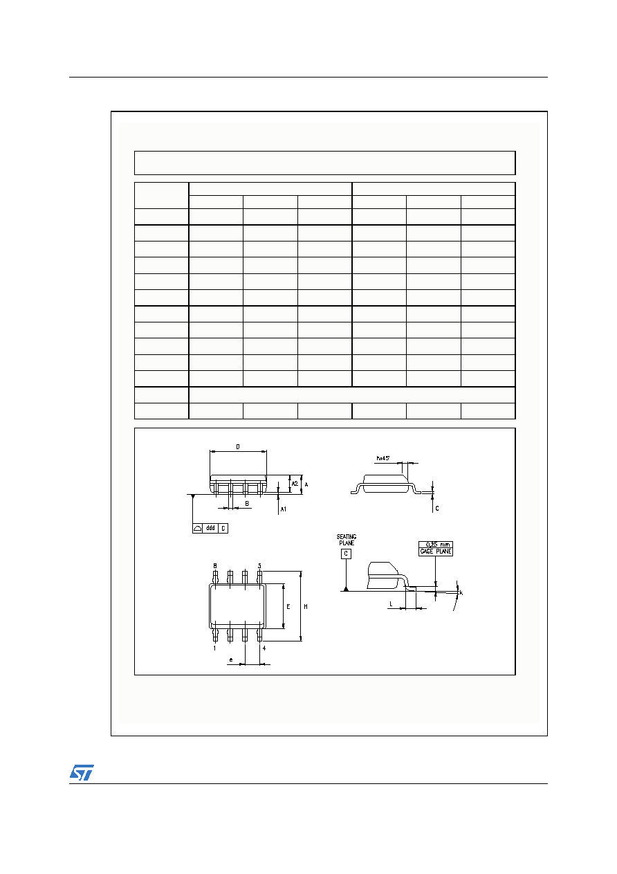
5.2 SO-8
Package
DIM.
mm.
inch
MIN.
TYP
MAX.
MIN.
TYP.
MAX.
A
1.35
1.75
0.053
0.069
A1
0.10
0.25
0.04
0.010
A2
1.10
1.65
0.043
0.065
B
0.33
0.51
0.013
0.020
C
0.19
0.25
0.007
0.010
D
4.80
5.00
0.189
0.197
E
3.80
4.00
0.150
0.157
e
1.27
0.050
H
5.80
6.20
0.228
0.244
h
0.25
0.50
0.010
0.020
L
0.40
1.27
0.016
0.050
k
∞ (max.)
ddd
0.1
0.04
SO-8 MECHANICAL DATA
0016023/C
8
Package Mechanical Data
LM358W-LM358AW
14/16
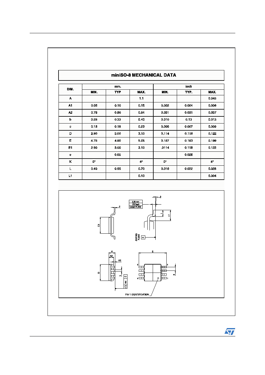
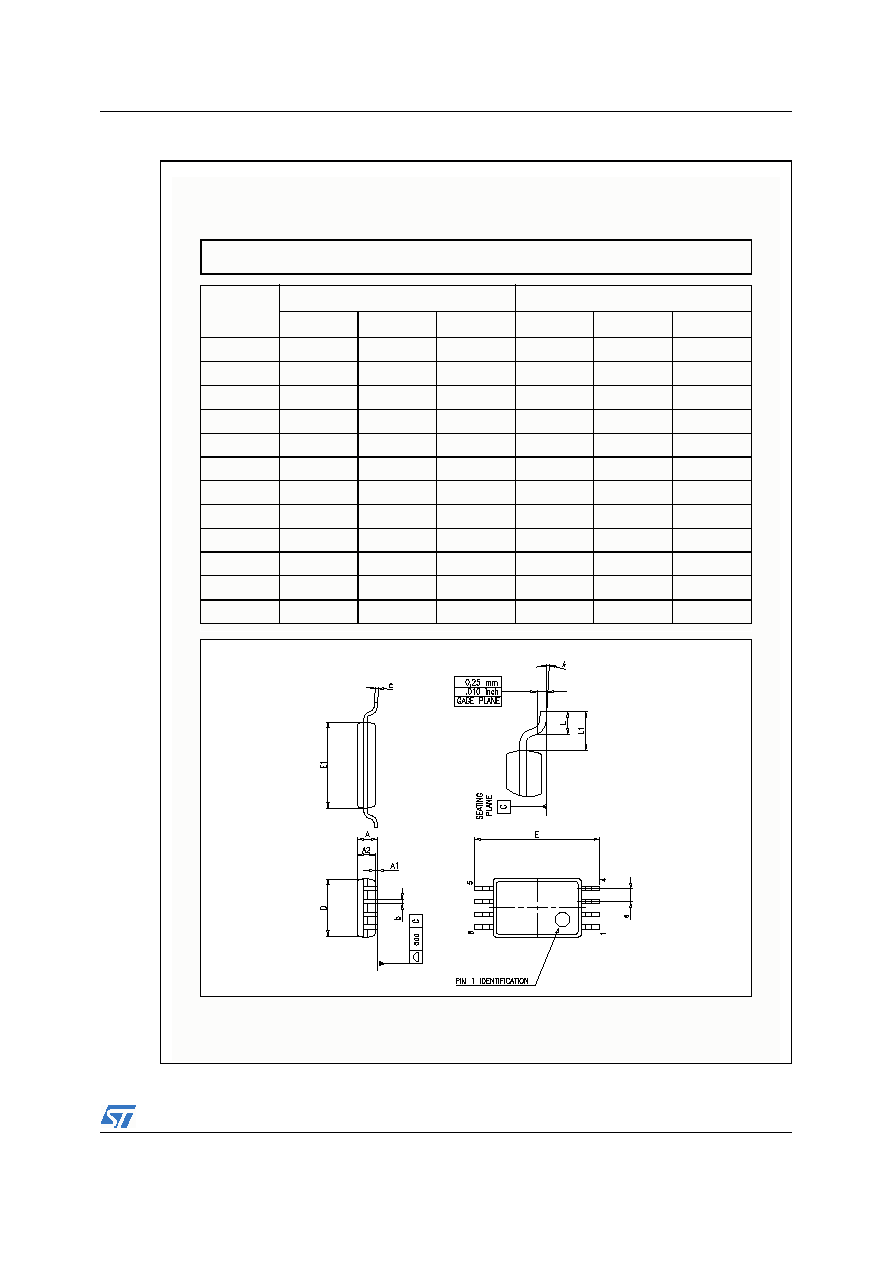
5.3 MiniSO-8
Package
LM358W-LM358AW
Package Mechanical Data
15/16
5.4 TSSOP8
Package
DIM.
mm.
inch
MIN.
TYP
MAX.
MIN.
TYP.
MAX.
A
1.2
0.047
A1
0.05
0.15
0.002
0.006
A2
0.80
1.00
1.05
0.031
0.039
0.041
b
0.19
0.30
0.007
0.012
c
0.09
0.20
0.004
0.008
D
2.90
3.00
3.10
0.114
0.118
0.122
E
6.20
6.40
6.60
0.244
0.252
0.260
E1
4.30
4.40
4.50
0.169
0.173
0.177
e
0.65
0.0256
K
0∞
8∞
0∞
8∞
L
0.45
0.60
0.75
0.018
0.024
0.030
L1
1
0.039
TSSOP8 MECHANICAL DATA
0079397/D

Revision History
LM358W-LM358AW
16/16
6 Revision
History
Date
Revision
Changes
Nov. 2002
1
First Release
July 2005
3
ESD protection inserted in
Table 1 on page 3
Information furnished is believed to be accurate and reliable. However, STMicroelectronics assumes no responsibility for the consequences
of use of such information nor for any infringement of patents or other rights of third parties which may result from its use. No license is
granted by implication or otherwise under any patent or patent rights of STMicroelectronics. Specifications mentioned in this publication are
subject to change without notice. This publication supersedes and replaces all information previously supplied. STMicroelectronics products
are not authorized for use as critical components in life support devices or systems without express written approval of STMicroelectronics.
The ST logo is a registered trademark of STMicroelectronics.
All other names are the property of their respective owners
© 2005 STMicroelectronics - All rights reserved
STMicroelectronics group of companies
Australia - Belgium - Brazil - Canada - China - Czech Republic - Finland - France - Germany - Hong Kong - India - Israel - Italy - Japan -
Malaysia - Malta - Morocco - Singapore - Spain - Sweden - Switzerland - United Kingdom - United States of America
www.st.com