1/20
July 2003
s
COMPLETE INTERFACE FOR TWO LNBs
REMOTE SUPPLY AND CONTROL
s
LNB SELECTION AND STAND-BY
FUNCTION
s
BUILT-IN TONE OSCILLATOR FACTORY
TRIMMED AT 22KHz
s
FAST OSCILLATOR START-UP FACILITATES
DiSEqC
TM
ENCODING
s
TWO SUPPLY INPUTS FOR LOWEST
DISSIPATION
s
BYPASS FUNCTION FOR SLAVE
OPERATION
s
LNB SHORT CIRCUIT PROTECTION AND
DIAGNOSTIC
s
AUXILIARY MODULATION INPUT EXTENDS
FLEXIBILITY
s
CABLE LENGTH COMPENSATION
s
INTERNAL OVER TEMPERATURE
PROTECTION
s
BACKWARD CURRENT PROTECTION
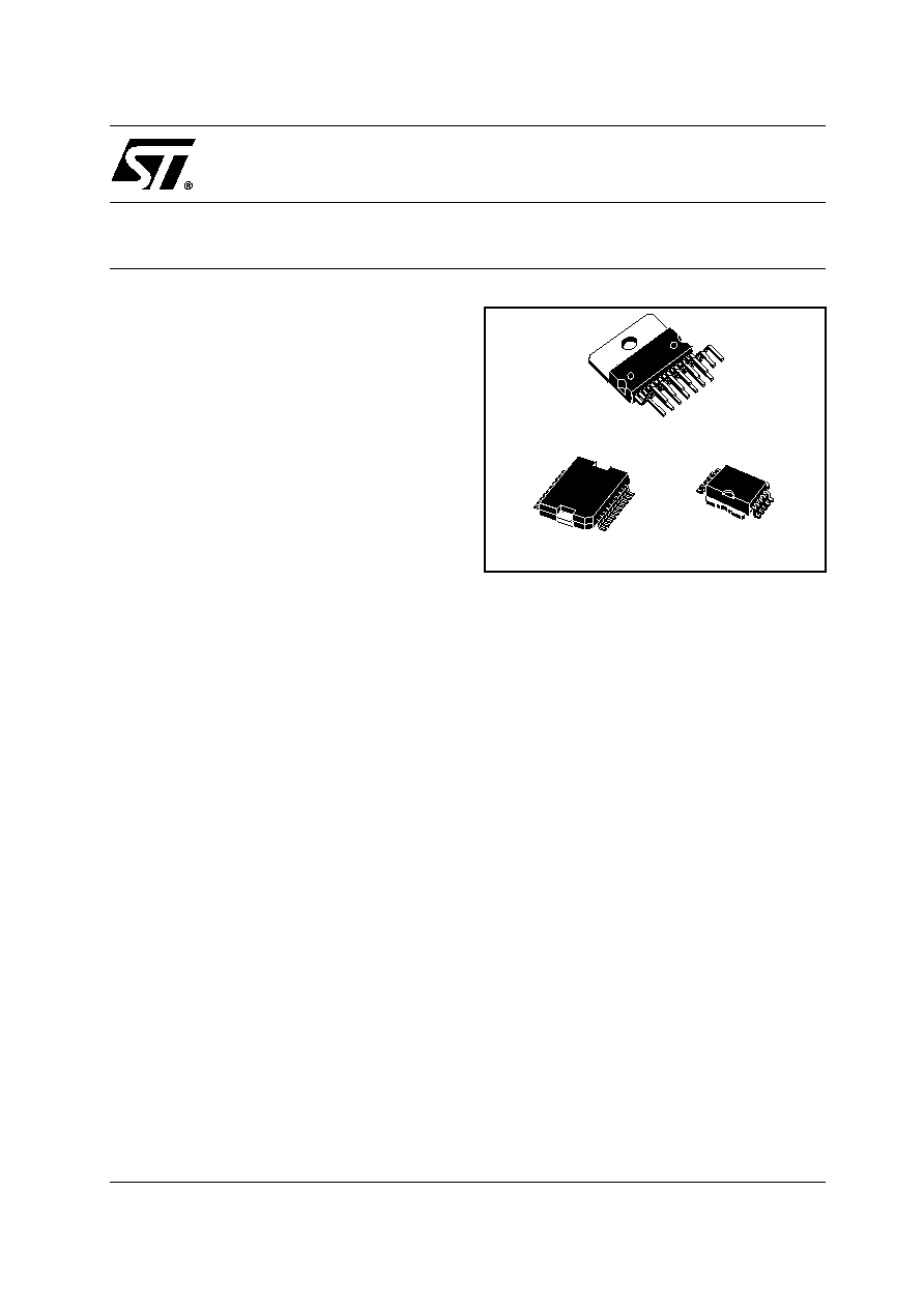
DESCRIPTION
Intended for analog and digital satellite receivers,
the LNBK is a monolithic linear voltage regulator,
assembled in Multiwatt-15, PowerSO-20 and
PowerSO-10, specifically designed to provide the
powering voltages and the interfacing signals to
the LNB downconverter situated in the antenna
via the coaxial cable. It has the same functionality
of the LNBP1X and LNBP20 series, at a reduced
output current capability. Since most satellite
receivers have two antenna ports, the output
voltage of the regulator is available at one of two
logic-selectable output pins (LNBA, LNBB). When
the IC is powered and put in Stand-by (EN pin
LOW), both regulator outputs are disabled to allow
the antenna downconverters to be supplied/
controlled by others satellite receivers sharing the
same coaxial lines. In this occurrence the device
will limit at 3 mA (max) the backward current that
could flow from LNBA and LNBB output pins to
GND.
For slave operation in single dish, dual receiver
systems, the bypass function is implemented by
an electronic switch between the Master Input pin
(MI) and the LNBA pin, thus leaving all LNB
powering and control functions to the Master
Receiver. This electronic switch is closed when
the device is powered and EN pin is LOW.
The regulator outputs can be logic controlled to be
13 or 18 V (typ.) by mean of the VSEL pin for
remote controlling of LNBs. Additionally, it is
possible to increment by 1V (typ.) the selected
voltage value to compensate the excess voltage
drop along the coaxial cable (LLC pin HIGH).
In order to reduce the power dissipation of the
device when the lowest output voltage is selected,
the regulator has two Supply Input pins V
CC1
and
V
CC2
. They must be powered respectively at 16V
(min) and 23V (min), and an internal switch
automatically will select the suitable supply pin
according to the selected output voltage. If
adequate heatsink is provided and higher power
losses are acceptable, both supply pins can be
powered by the same 23V source without
affecting any other circuit performance.
The ENT (Tone Enable) pin activates the internal
oscillator so that the DC output is modulated by a
±0.3 V, 22KHz (typ.) square wave. This internal
oscillator is factory trimmed within a tolerance of
±2KHz, thus no further adjustments neither
external components are required.
A burst coding of the 22KHz tone can be
accomplished thanks to the fast response of the
ENT input and the prompt oscillator start-up. This
helps designers who want to implement the
DiSEqC
TM
protocols (*).
LNBK10 SERIES
LNBK20
LNB SUPPLY AND CONTROL VOLTAGE
REGULATOR (PARALLEL INTERFACE)
PowerSO-10
1
10
PowerSO-20
Multiwatt-15
LNBK10 SERIES - LNBK20
2/20
In order to improve design flexibility and to allow
implementation of newcoming LNB remote control
standards, an analogic modulation
input pin is available (EXTM). An appropriate DC
blocking capacitor must be used to couple the
modulating signal source to the EXTM pin. When
external modulation is not used, the relevant pin
can be left open.
Two pins are dedicated to the overcurrent
protection/monitoring:
CEXT
and
OLF.
The
overcurrent protection circuit works dynamically:
as soon as an overload is detected in either LNB
output, the output is shut-down for a time Toff
determined by the capacitor connected between
CEXT and GND. Simultaneously the OLF pin, that
is an open collector diagnostic output flag, from
HIGH IMPEDANCE state goes LOW.
After the time has elapsed, the output is resumed
for a time t
on
=1/15t
off
(typ.) and OLF goes in HIGH
IMPEDANCE. If the overload is still present, the
protection circuit will cycle again through t
off
and
ton until the overload is removed. Typical t
on
+t
off
value is 1200ms when a 4.7
µ
F external capacitor
is used.
This dynamic operation can greatly reduce the
power dissipation in short circuit condition, still
ensuring excellent power-on start up even with
highly capacitive loads on LNB outputs.
The device is packaged in Multiwatt15 for
thru-holes mounting and in PowerSO-20 for
surface mounting. When a limited functionality in a
smaller package matches design needs, a range
of cost-effective PowerSO-10 solutions is also
offered.
All
versions
have
built-in
thermal
protection against overheating damage.
(*): External components are needed to comply to level 2.x and above (bidirectional) DiSEqC
TM
bus hardware requirements. DiSEqC
TM
is a
trademark or EUTELSAT.
ORDERING CODES
(*) Available on request
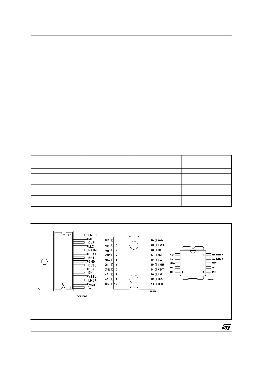
PIN CONFIGUARATION (top view)
TYPE
Multiwatt-15
PowerSO-20
PowerSO-10
LNBK10
LNBK10SP-TR (*)
LNBK11
LNBK11SP-TR (*)
LNBK12
LNBK12SP-TR (*)
LNBK13
LNBK13SP-TR (*)
LNBK14
LNBK14SP-TR (*)
LNBK15
LNBK15SP-TR (*)
LNBK16
LNBKP16SP-R (*)
LNBK20
LNBK20CR
LNBK20PD-TR
PowerSo-20
PowerSO-10
Multiwatt-15
LNBK10 SERIES - LNBK20
3/20
TABLE A: PIN CONFIGURATIONS
NOTE: the limited pin availability of the PowerSO-10 package leads to drop some functions.
SYMBOL
NAME
FUNCTION
PIN NUMBER vs SALES TYPE (LNBK)
20CR 20PD 10SP 11SP 12SP 13SP 14SP 15SP 16SP
V
CC1
Supply Input 1 15V to 27V supply. It is
automatically selected
when V
OUT
= 13 or 14V
1
2
1
1
1
1
1
1
V
CC2
Supply Input 2 22V to 27V supply. It is
automatically selected
when V
OUT
= 18 or 19V
2
3
2
2
2
2
2
2
2
LNBA
Output Port
See truth table voltage
and port selection. In
stand-by mode this port
is powered by the MI pin
via the internal Bypass
Switch
3
4
3
3
3
3
3
3
3
V
SEL
Output Voltage
Selection:13 or
18V (typ)
Logic control input: see
truth table
4
5
4
4
4
4
4
4
4
EN
Port Enable
Logic control input: see
truth table
5
6
5
5
5
5
5
5
5
OSEL
Port Selection Logic control input: see
truth table
7
7
9
NA
NA
NA
NA
NA
NA
GND
Ground
Circuit Ground. It is
internally connected to
the die frame
8
1
10
11
20
6
6
6
6
6
6
ENT
22KHz Tone
Enable
Logic control input: see
truth table
9
13
7
7
7
7
7
7
7
CEXT
External
Capacitor
Timing Capacitor used
by the Dynamic
Overload protection.
Typical application is
4.7
µ
F for a 1200ms
cycle
10
14
8
8
8
8
8
8
8
EXTM
External
Modulator
External Modulation
Input. Needs DC
decoupling to the AC
source. if not used, can
be left open.
11
15
NA
NA
NA
9
NA
9
9
LLC
Line Length
Compens.
(1V typ)
Logic control input: see
truth table
12
16
NA
NA
9
NA
9
NA
10
OLF
Over Load
Flag
Logic output (open
collector). Normally in
HIGH IMPEDANCE,
goes LOW when current
or thermal overload
occurs
13
17
NA
9
NA
NA
10
10
NA
MI
Master Input
In stand-by mode, the
voltage on MI is routed
to LNBA pin. Can be left
open if bypass function
is not needed
14
18
NA
10
10
10
NA
NA
NA
LNBB
Output Port
See truth tables for
voltage and port
selection
15
19
10
NA
NA
NA
NA
NA
NA
LNBK10 SERIES - LNBK20
4/20
ABSOLUTE MAXIMUM RATINGS
Absolute Maximum Ratings are those values beyond which damage to the device may occur. Functional operation under these condition is
not implied.
THERMAL DATA
LOGIC CONTROLS TRUTH TABLE
NOTE: All logic input pins have internal pull-down resistor (typ. = 250K
)
Symbol
Parameter≤
Value
Unit
V
I
DC Input Voltage (V
CC1
, V
CC2
, MI)
28
V
I
O
Output Current (LNBA, LNBB)
Internally Limited
mA
V
I
Logic Input Voltage (ENT, EN OSEL, VSEL, LLC)
-0.5 to 7
V
I
SW
Bypass Switch Current
900
mA
P
D
Power Dissipation at T
case
< 85∞C
14
W
T
stg
Storage Temperature Range
-40 to +150
∞C
T
op
Operating Junction Temperature Range
-40 to +125
∞C
Symbol
Parameter
Value
Unit
R
thj-case
Thermal Resistance Junction-case
2
∞C/W
CONTROL I/O
PIN NAME
L
H
OUT
OLF
I
OUT
> I
OMAX
or T
j
> 150∞C
I
OUT
< I
OMAX
IN
ENT
22KHz tone OFF
22KHz tone ON
IN
EN
See Table Below
See Table Below
IN
OSEL
See Table Below
See Table Below
IN
VSEL
See Table Below
See Table Below
IN
LLC
See Table Below
See Table Below
EN
OSEL
VSEL
LLCO
V
LNBA
V
LNBB
L
X
X
X
V
MI
- 0.4V (typ.)
Disabled
H
L
L
L
13V (typ.)
Disabled
H
L
H
L
18V (typ.)
Disabled
H
L
L
H
14V (typ.)
Disabled
H
L
H
H
19V (typ.)
Disabled
H
H
L
L
Disabled
13V (typ.)
H
H
H
L
Disabled
18V (typ.)
H
H
L
H
Disabled
14V (typ.)
H
H
H
H
Disabled
19V (typ.)
LNBK10 SERIES - LNBK20
5/20
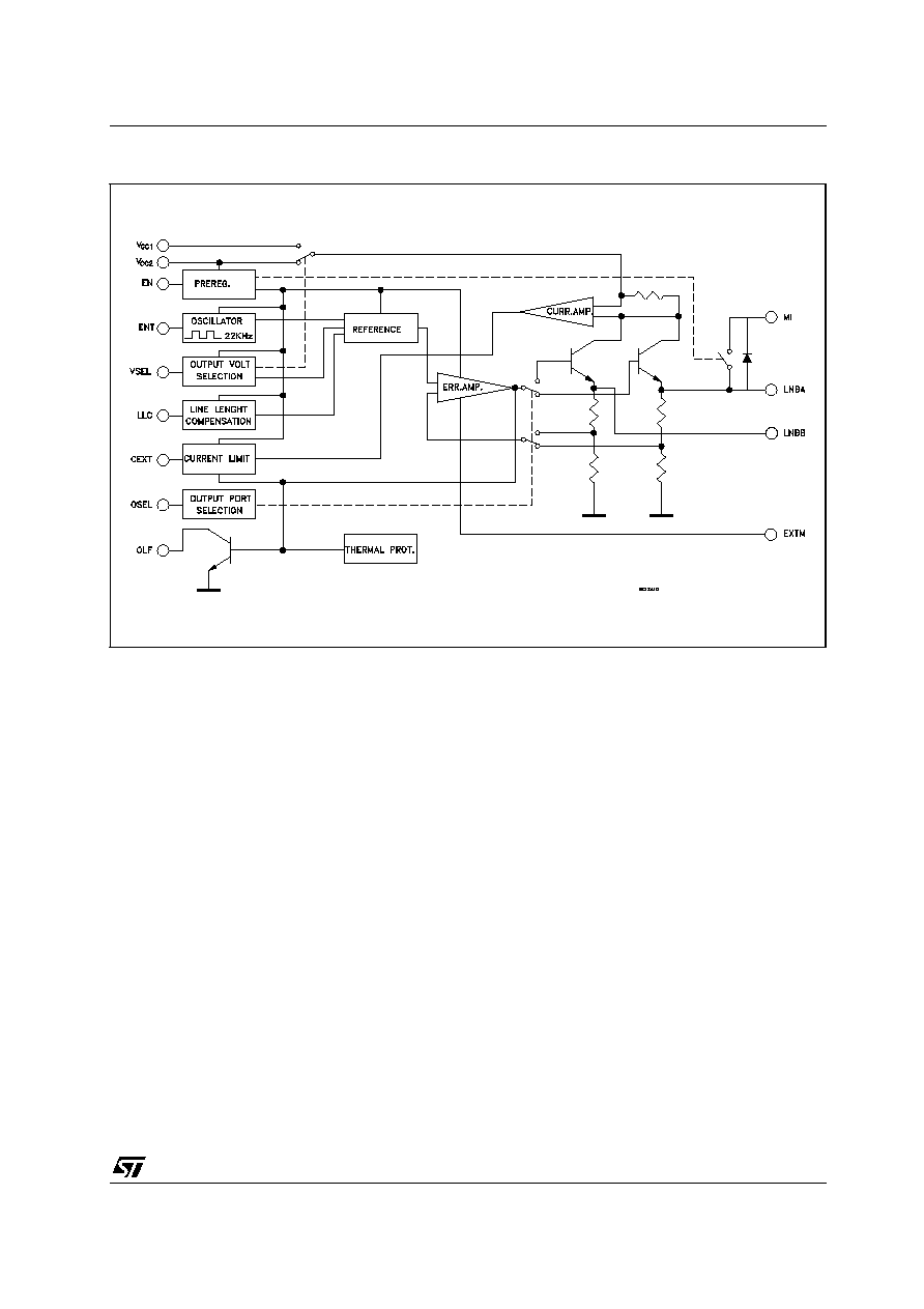
BLOCK DIAGRAM
LNBK10 SERIES - LNBK20
6/20
ELECTRICAL CHARACTERISTICS FOR LNBK SERIES (T
J
= 0 to 85∞C, C
I
= 0.22
µ
F, C
O
=0.1
µ
F,
EN=H, ENT=L, LLC=L, V
IN1
=16V, V
IN2
=23V I
OUT
=50mA, unless otherwise specified.)
Symbol
Parameter
Test Conditions
Min.
Typ.
Max.
Unit
V
IN1
V
CC1
Supply Voltage
I
O
= 400 mA ENT=H, VSEL=L, LLC=L
15
27
V
I
O
= 400 mA ENT=H, VSEL=L, LLC=H
16
27
V
V
IN2
V
CC2
Supply Voltage
I
O
= 400 mA ENT=H, VSEL=L, LLC=L
22
27
V
I
O
= 400 mA VSEL=L, LLC=H
23
27
V
V
O1
Output Voltage
I
O
= 400 mA VSEL=L, LLC=L
17.3
18
18.7
V
I
O
= 400 mA ENT=H, VSEL=L, LLC=H
19
V
V
O2
Output Voltage
I
O
= 400 mA VSEL=L, LLC=L
12.5
13
13.5
V
I
O
= 400 mA ENT=H, VSEL=L, LLC=H
14
V
V
O
Line Regulation
V
IN1
=15 to 18V
V
OUT
=13V
5
50
mV
V
IN2
=22 to 25V
V
OUT
=18V
5
50
mV
V
O
Load Regulation
V
IN1
=V
IN2
=22V
V
OUT
=13 or 18V
I
O
= 0 to 3A
65
150
mV
SVR
Supply Voltage Rejection
V
IN1
= V
IN2
= 23
±
0.5V
ac
f
ac
= 120 Hz,
45
dB
I
MAX
Output Current Limiting
500
650
800
mA
t
OFF
Dynamic Overload
protection OFF Time
Output Shorted
C
EXT
=4.7
µ
F
1100
ms
t
ON
Dynamic Overload
protection ON Time
Output Shorted
C
EXT
=4.7
µ
F
t
OFF
/15
ms
f
TONE
Tone Frequency
ENT=H
20
22
24
KHz
A
TONE
Tone Amplitude
ENT=H
0.55
0.72
0.9
Vpp
D
TONE
Tone Duty Cycle
ENT=H
40
50
60
%
t
r
, t
f
Tone Rise and Fall Time
ENT=H
5
10
15
µ
s
G
EXTM
External Modulation Gain
V
OUT
/
V
EXTM
,
f = 10Hz to 40KHz
5
V
EXTM
External Modulation Input
Voltage
AC Coupling
400
mVpp
Z
EXTM
External Modulation
Impedance
f = 10Hz to 40KHz
400
V
SW
Bypass Switch Voltage
Drop (MI to LNBA)
EN=L,
I
SW
=300mA,
V
CC2
-V
MI
=4V
0.35
0.6
V
V
OL
Overload Flag Pin Logic
LOW
I
OL
=8mA
0.28
0.5
V
I
OZ
Overload Flag Pin OFF
State Leakage Current
V
OH
= 6V
10
µ
A
V
IL
Control Input Pin Logic
LOW
0.8
V
V
IH
Control Input Pin Logic
HIGH
2.5
V
I
IH
Control Pins Input Current
V
IH
= 5V
20
µ
A
I
CC
Supply Current
Output Disabled (EN=L)
0.3
1
mA
ENT=H,
I
OUT
=500mA
3.1
6
mA
I
OBK
Output Backward Current
EN=L
V
LNBA
= V
LNBB
= 18V
V
IN1
= V
IN2
= 22V or floating
0.2
3
mA
T
SHDN
Temperature Shutdown
Threshold
150
∞C
LNBK10 SERIES - LNBK20
7/20
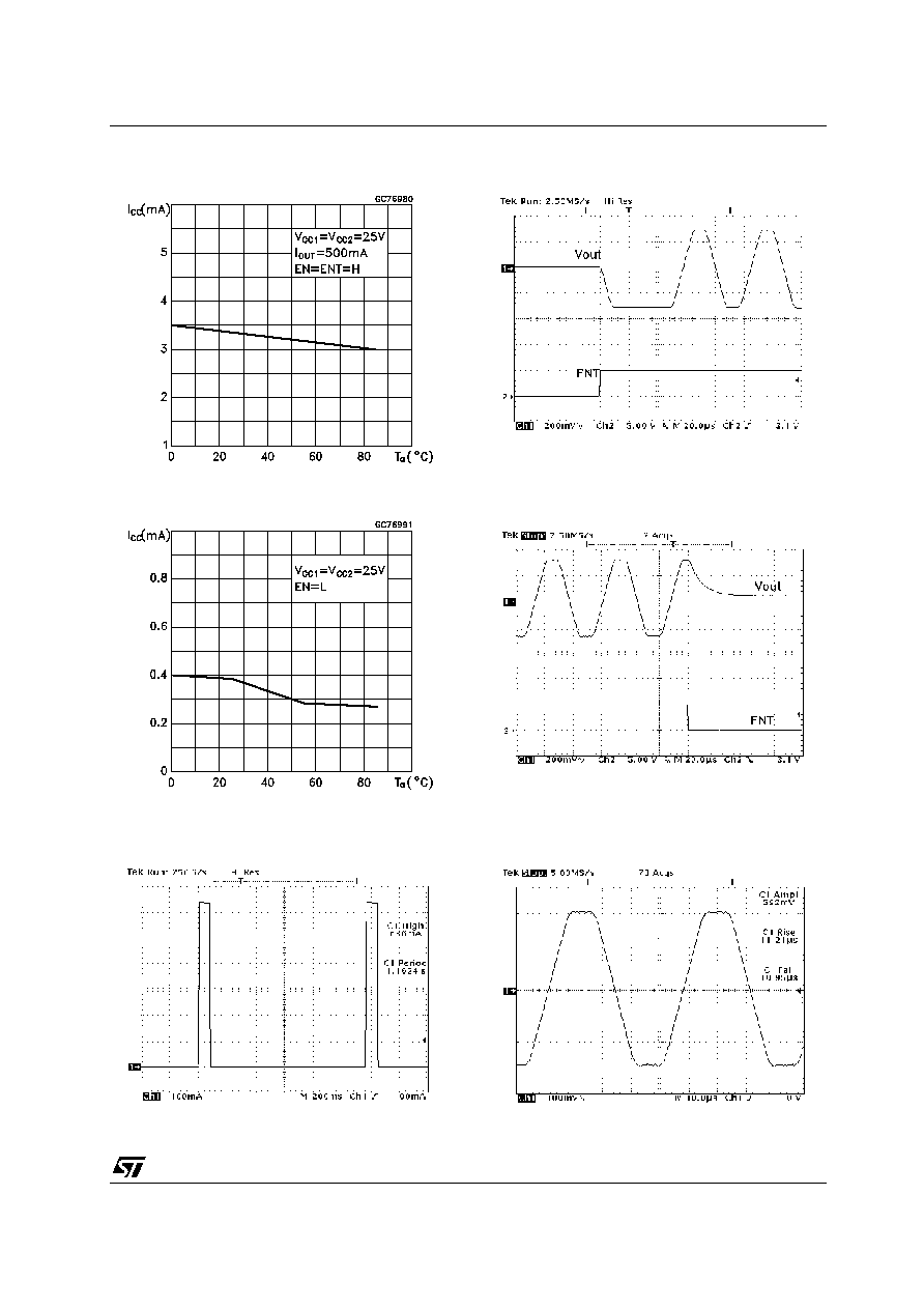
TYPICAL CHARACTERISTICS (unless otherwise specified T
j
= 25∞C)
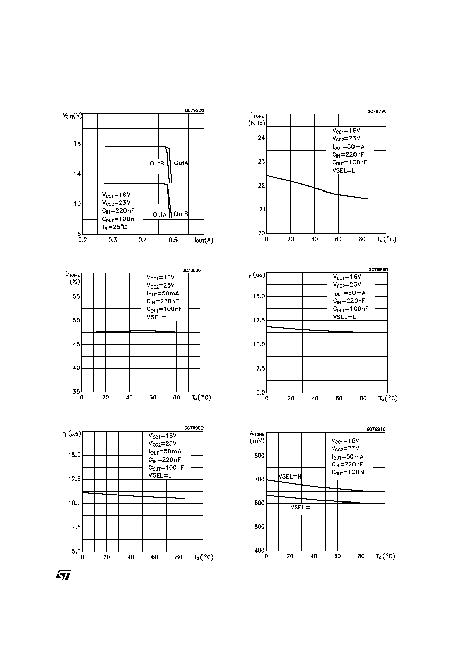
Figure 1 : Output Voltage vs Output Current
Figure 2 : Tone Duty Cycle vs Temperature
Figure 3 : Tone Fall Time vs Temperature
Figure 4 : Tone Frequency vs Temperature
Figure 5 : Tone Rise Time vs Temperature
Figure 6 : Tone Amplitude vs Temperature
LNBK10 SERIES - LNBK20
8/20
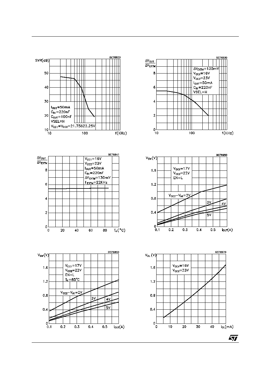
Figure 7 : S.V.R. vs Frequency
Figure 8 : External Modulation vs Temperature
Figure 9 : Bypass Switch Drop vs Output Current
Figure 10 : LNBA External Modulation gain vs
Frequency
Figure 11 : Bypass switch Drop vs Output
Current
Figure 12 : overload Flag pin Logic LOW vs Flag
Current
LNBK10 SERIES - LNBK20
9/20
Figure 13 : Supply Voltage vs Temperature
Figure 14 : Supply Current vs Temperature
Figure 15 : Dynamic Overload protection (I
SC
vs
Time)
Figure 16 : Tone Enable
Figure 17 : Tone Disable
Figure 18 : 22KHz Tone
LNBK10 SERIES - LNBK20
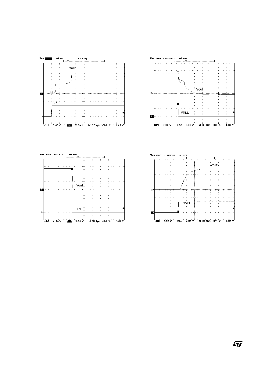
10/20
Figure 19 : Enable Time
Figure 20 : Disable Time
Figure 21 : 18V to 13V Change
Figure 22 : 18V to 13V Change
LNBK10 SERIES - LNBK20
11/20
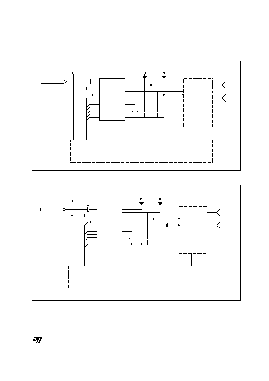
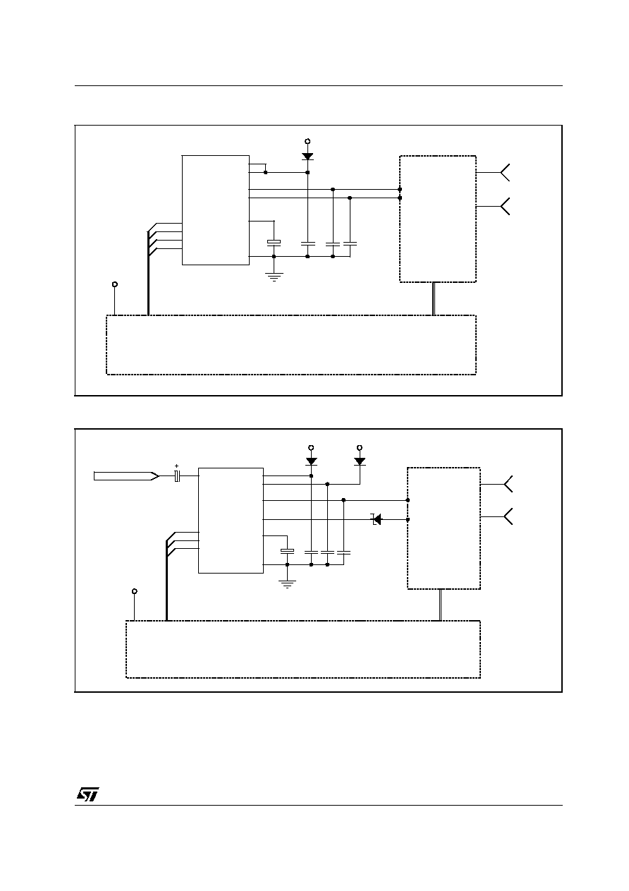
TYPICAL APPLICATION SCHEMATICS
TWO ANTENNA PORTS RECEIVER
SINGLE ANTENNA RECEIVER WITH MASTER RECEIVER PORT
JA
JB
ANT CONNECTORS
17V
24V
MCU+V
VCC1
1
VCC2
2
LNBA
3
LNBB
15
GND
8
LLC
12
EXTM
11
OSEL
7
EN
5
ENT
9
VSEL
4
OLF
13
MI
14
CEXT
10
LNBP20CR
C2
10uF
R1
47K
AUX DATA
C3
2x 0.1µF
C1
4.7µF
C4
C6
C5
2x 47nF
TUNER
I/Os
MCU
I/Os
Vcc
+
24V
17V
MCU+V
VCC1
1
VCC2
2
LNBA
3
LNBB
15
GND
8
LLC
12
EXTM
11
OSEL
7
EN
5
ENT
9
VSEL
4
OLF
13
MI
14
CEXT
10
LNBP20CR
C2
10uF
AUX DATA
R1
47K
TUNER
ANT
MASTER
C4
C5
47nF
C3
2x 0.1µF
C1
4.7µF
I/Os
Vcc
MCU
I/Os
+
LNBK10 SERIES - LNBK20
12/20
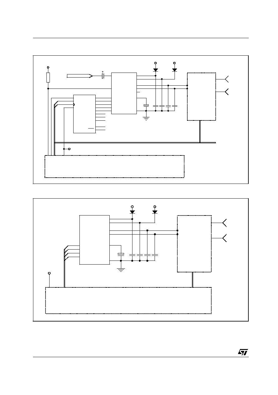
USING SERIAL BUS TO SAVE MPU I/Os
TWO ANTENNA PORTS RECEIVER: LOW COST SOLUTION
VCC1
1
VCC2
2
LNBA
3
LNBB
15
GND
8
LLC
12
EXTM
11
OSEL
7
EN
5
ENT
9
VSEL
4
OLF
13
MI
14
CEXT
10
LNBP20CR
C2
10uF
MCU+V
R1
47K
AUX DATA
STR
1
D
2
CLK
3
OE
15
Q1
4
Q2
5
Q3
6
Q4
7
Q5
14
Q6
13
Q7
12
Q8
11
QS
9
QS
10
4094
TUNER
JA
JB
ANT
CONNECTORS
C4
C6
C5
2x 47nF
C3
2x 0.1µF
C1
4.7µF
MCU+V
SERIAL
BUS
MCU
I/Os
Vcc
+
17V
24V
JA
JB
ANT CONNECTORS
17V
24V
VCC1
1
VCC2
2
LNBA
3
LNBB
10
GND
6
CEXT
8
OSEL
9
EN
5
ENT
7
VSEL
4
LNBP10SP
C3
2x 0.1µF
C1
4.7µF
C4
C6
C5
2x 47nF
TUNER
I/Os
MCU
MCU+V
I/Os
Vcc
+
LNBK10 SERIES - LNBK20
13/20
CONNECTING TOGETHER V
CC1
AND V
CC2
SINGLE ANTENNA RECEIVER WITH MASTER RECEIVER PORT: LOW COST SOLUTION
JA
JB
ANT CONNECTORS
24V
VCC1
1
VCC2
2
LNBA
3
LNBB
10
GND
6
CEXT
8
OSEL
9
EN
5
ENT
7
VSEL
4
LNBP10SP
C1
4.7µF
C6
C5
2x 47nF
C4
0.1µF
TUNER
I/Os
MCU
MCU+V
I/Os
Vcc
+
24V
17V
VCC1
1
VCC2
2
LNBA
3
MI
10
GND
6
CEXT
8
EXTM
9
EN
5
ENT
7
VSEL
4
LNBP13SP
C2
10µF
AUX DATA
TUNER
ANT
MASTER
C4
C5
47nF
C3
2x 0.1µF
C1
4.7µF
MCU+V
I/Os
Vcc
MCU
I/Os
+
LNBK10 SERIES - LNBK20
14/20
SINGLE ANTENNA RECEIVER WITH OVERLOAD DIAGNOSTIC
24V
17V
MCU+V
C2
10µF
VCC1
1
VCC2
2
LNBA
3
GND
6
CEXT
8
EXTM
9
EN
5
ENT
7
VSEL
4
OLF
10
LNBP15SP
AUX DATA
R1
47K
TUNER
ANT
C4
C5
47nF
C3
2x 0.1µF
C1
4.7µF
Vcc
I/Os
MCU
I/Os
+
LNBK10 SERIES - LNBK20
15/20
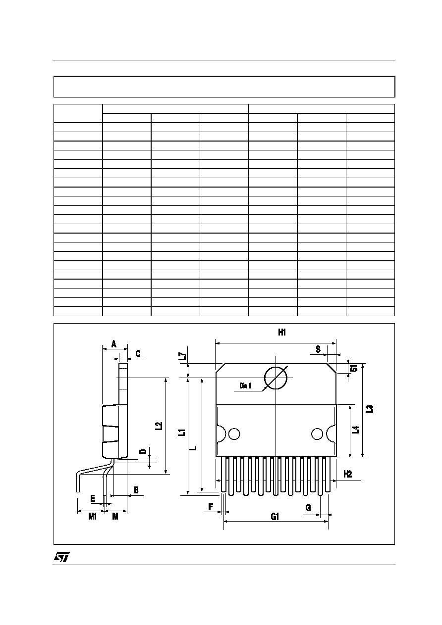
DIM.
mm.
inch
MIN.
TYP
MAX.
MIN.
TYP.
MAX.
A
5
0.197
B
2.65
0.104
C
1.6
0.063
D
1
0.039
E
0.49
0.55
0.019
0.022
F
0.66
0.75
0.026
0.030
G
1.02
1.27
1.52
0.040
0.050
0.060
G1
17.53
17.78
18.03
0.690
0.700
0.710
H1
19.6
0.772
H2
20.2
0.795
L
21.9
22.2
22.5
0.862
0.874
0.886
L1
21.7
22.1
22.5
0.854
0.870
0.886
L2
17.65
18.1
0.695
0.713
L3
17.25
17.5
17.75
0.679
0.689
0.699
L4
10.3
10.7
10.9
0.406
0.421
0.429
L7
2.65
2.9
0.104
0.114
M
4.25
4.55
4.85
0.167
0.179
0.191
M1
4.63
5.08
5.53
0.182
0.200
0.218
S
1.9
2.6
0.075
0.102
S1
1.9
2.6
0.075
0.102
Dia1
3.65
3.85
0.144
0.152
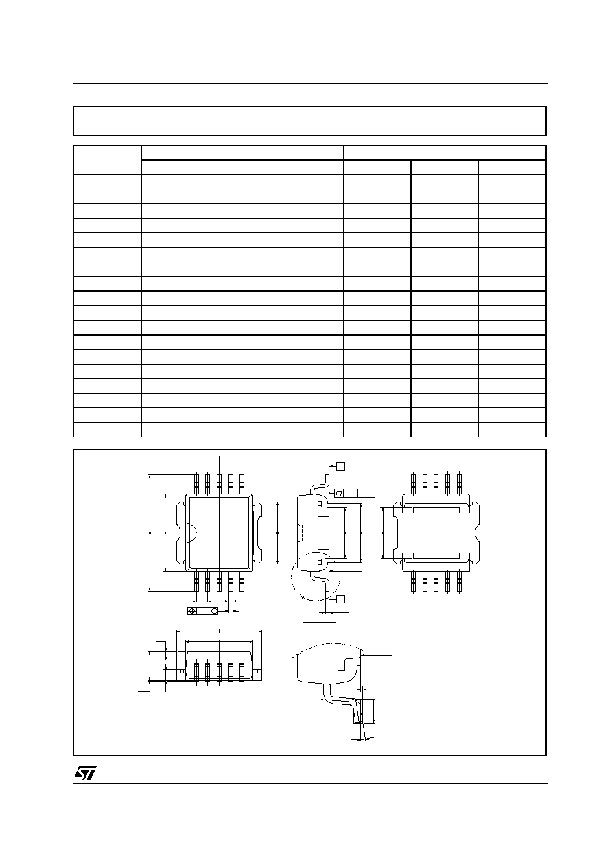
MULTIW ATT-15 MECHANICAL DATA
0016036
LNBK10 SERIES - LNBK20
16/20
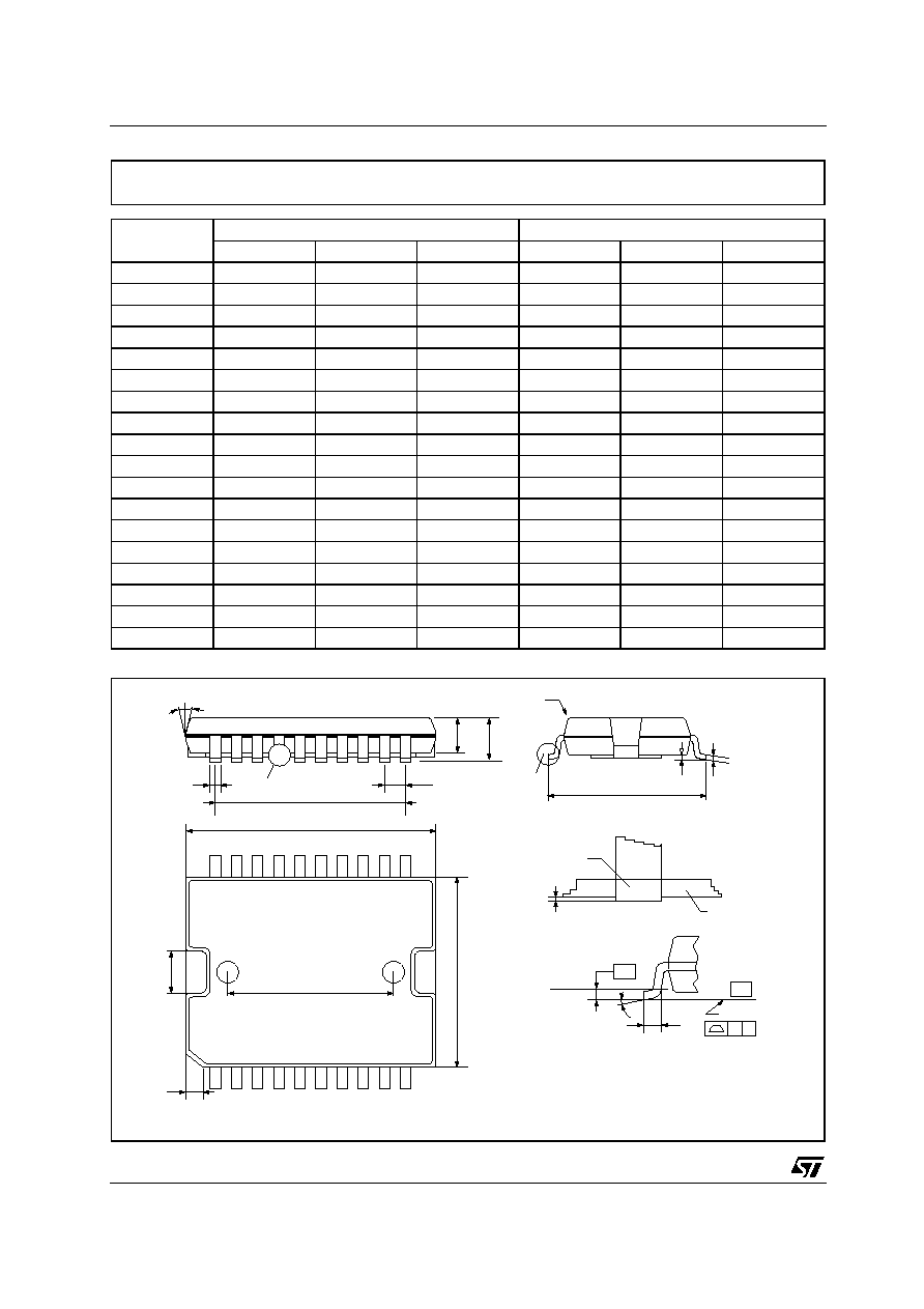
DIM.
mm.
inch
MIN.
TYP
MAX.
MIN.
TYP.
MAX.
A
3.60
0.1417
a1
0.10
0.30
0.0039
0.0118
a2
3.30
0.1299
a3
0
0.10
0
0.0039
b
0.40
0.53
0.0157
0.0209
c
0.23
0.32
0.0090
0.0013
D (1)
15.80
16.00
0.6220
0.630
E
13.90
14.50
0.5472
0.5710
e
1.27
0.0500
e3
11.43
0.4500
E1 (1)
10.90
11.10
0.4291
0.4370
E2
2.90
0.1141
G
0
0.10
0.0000
0.0039
h
1.10
0.0433
L
0.80
1.10
0.0314
0.0433
N
0∞
10∞
S
0∞
8∞
0∞
8∞
T
10.0
0.3937
PowerSO-20 MECHANICAL DATA
0056635
e
a2
A
E
a1
PSO20MEC
DETAIL A
T
D
1
1
0
11
20
E1
E2
h x 45∞
DETAIL A
lea
d
slug
a3
S
Gage
Plan
e
0.35
L
DETAIL B
R
DETAIL B
(COPLANARITY)
G
C
- C -
SEATING PLANE
e3
b
c
N
N
(1) "D and E1" do not include mold flash or protusions - Mold flash or protusions shall not exceed 0.15mm (0.006")
1
LNBK10 SERIES - LNBK20
17/20
DIM.
mm.
inch
MIN.
TYP
MAX.
MIN.
TYP.
MAX.
A
3.35
3.65
0.132
0.144
A1
0.00
0.10
0.000
0.004
B
0.40
0.60
0.016
0.024
c
0.35
0.55
0.013
0.022
D
9.40
9.60
0.370
0.378
D1
7.40
7.60
0.291
0.300
E
9.30
9.50
0.366
0.374
E1
7.20
7.40
0.283
0.291
E2
7.20
7.60
0.283
0.300
E3
6.10
6.35
0.240
0.250
E4
5.90
6.10
0.232
0.240
e
1.27
0.050
F
1.25
1.35
0.049
0.053
H
13.80
14.40
0.543
0.567
h
0.50
0.002
L
1.20
1.80
0.047
0.071
q
1.70
0.067
0∞
8∞
PowerSO-10 MECHANICAL DATA
0068039-C
DETAIL "A"
PLANE
SEATING
L
A1
F
A1
h
A
D
D1
= =
= =
= =
E4
0.10 A
E1
E3
C
Q
A
= =
B
B
DETAIL "A"
SEATING
PLANE
= =
= =
E2
6
10
5
1
e
B
H
E
M
0.25
= =
= =
LNBK10 SERIES - LNBK20
18/20
DIM.
mm.
inch
MIN.
TYP
MAX.
MIN.
TYP.
MAX.
A
330
12.992
C
12.8
13.2
0.504
0.519
D
20.2
0.795
N
60
2.362
T
30.4
1.197
Ao
15.1
15.3
0.594
0.602
Bo
16.5
16.7
0.650
0.658
Ko
3.8
4.0
0.149
0.157
Po
3.9
4.1
0.153
0.161
P
23.9
24.1
0.941
0.949
W
23.7
24.3
0.933
0.957
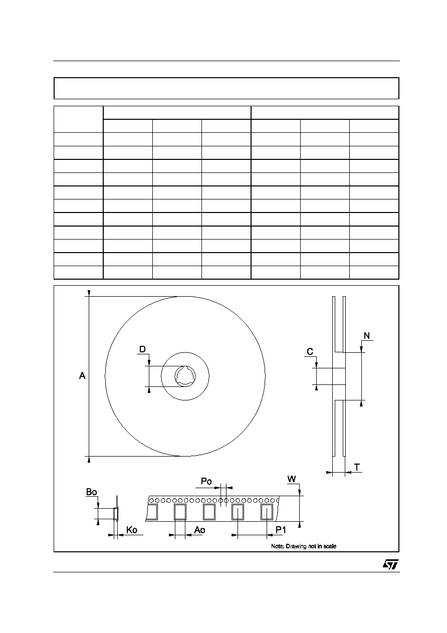
Tape & Reel PowerSO-20 MECHANICAL DATA
LNBK10 SERIES - LNBK20
19/20
DIM.
mm.
inch
MIN.
TYP
MAX.
MIN.
TYP.
MAX.
A
330
12.992
C
12.8
13.2
0.504
0.519
D
20.2
0.795
N
60
2.362
T
30.4
1.197
Ao
14.9
15.1
0.587
0.594
Bo
9.9
10.1
0.390
0.398
Ko
4.15
4.35
0.163
0.171
Po
3.9
4.1
0.153
0.161
P
23.9
24.1
0.941
0.949
W
23.7
24.3
0.933
0.957
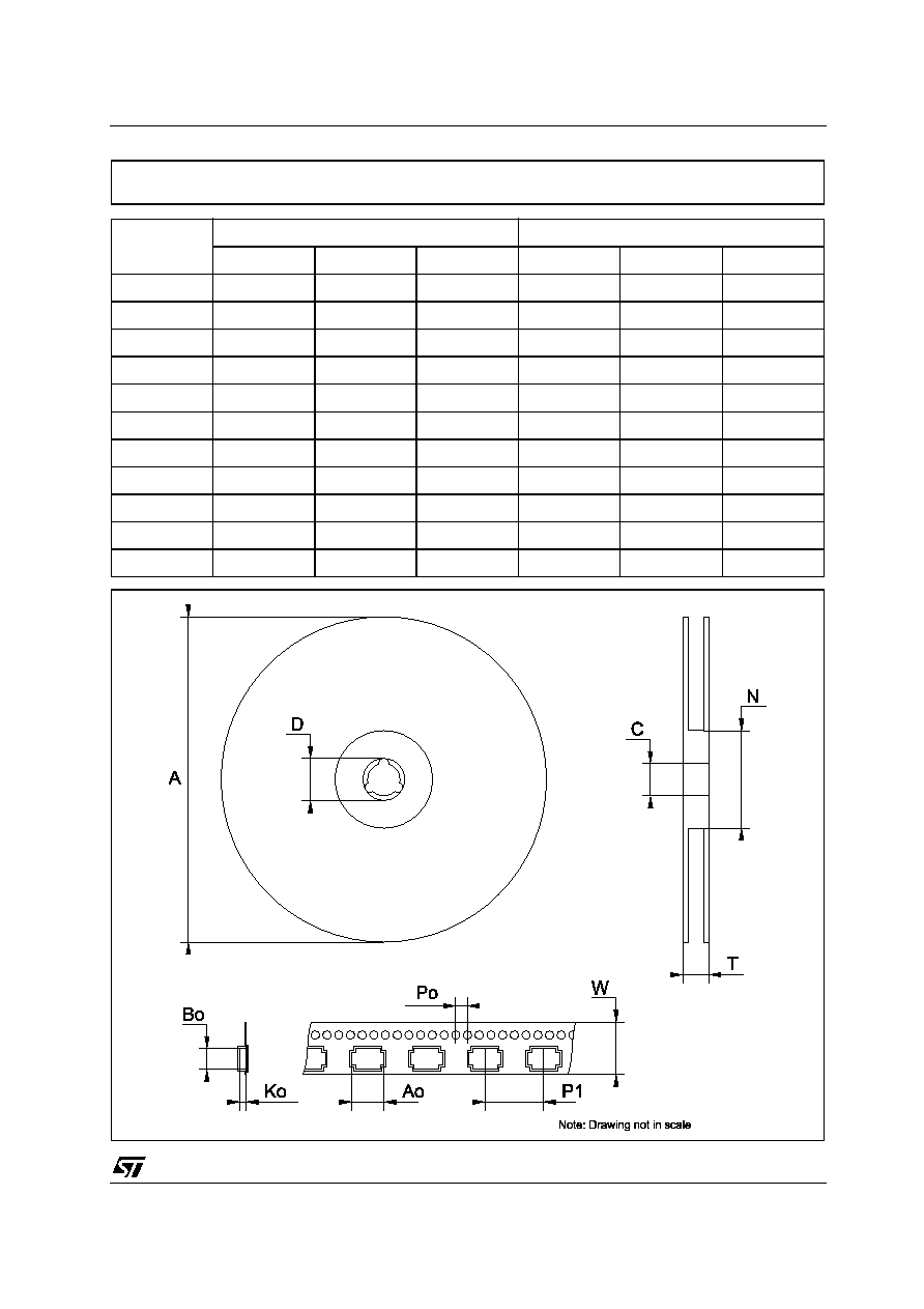
Tape & Reel PowerSO10 MECHANICAL DATA

LNBK10 SERIES - LNBK20
20/20
Information furnished is believed to be accurate and reliable. However, STMicroelectronics assumes no responsibility for the
consequences of use of such information nor for any infringement of patents or other rights of third parties which may result from
its use. No license is granted by implication or otherwise under any patent or patent rights of STMicroelectronics. Specifications
mentioned in this publication are subject to change without notice. This publication supersedes and replaces all information
previously supplied. STMicroelectronics products are not authorized for use as critical components in life support devices or
systems without express written approval of STMicroelectronics.
© The ST logo is a registered trademark of STMicroelectronics
© 2003 STMicroelectronics - Printed in Italy - All Rights Reserved
STMicroelectronics GROUP OF COMPANIES
Australia - Brazil - Canada - China - Finland - France - Germany - Hong Kong - India - Israel - Italy - Japan - Malaysia - Malta - Morocco
Singapore - Spain - Sweden - Switzerland - United Kingdom - United States.
© http://www.st.com