 | –≠–ª–µ–∫—Ç—Ä–æ–Ω–Ω—ã–π –∫–æ–º–ø–æ–Ω–µ–Ω—Ç: LNBP9 | –°–∫–∞—á–∞—Ç—å:  PDF PDF  ZIP ZIP |
1/8
November 2004
s
SIMPLEST INTEGRATED SOLUTION FOR
THE LNB REMOTE SUPPLY AND CONTROL
s
500mA GUARANTEED OUTPUT CURRENT
s
DUAL INPUT SUPPLY FOR REDUCING
POWER DISSIPATION
s
22KHZ BUILT-IN TONE OSCILLATOR
(LNBP9 VERSION)
s
FAST OSCILLATOR START-UP FOR
DiSEqC
TM
ENCODING (LNBP9 VERSION)
s
AUXILIARY MODULATION INPUT FOR
MORE FLEXIBILITY (LNBP8 VERSION)
s
STAND-BY FUNCTION
s
SHORT CIRCUIT AND
OVERTEMPERATURE PROTECTION
s
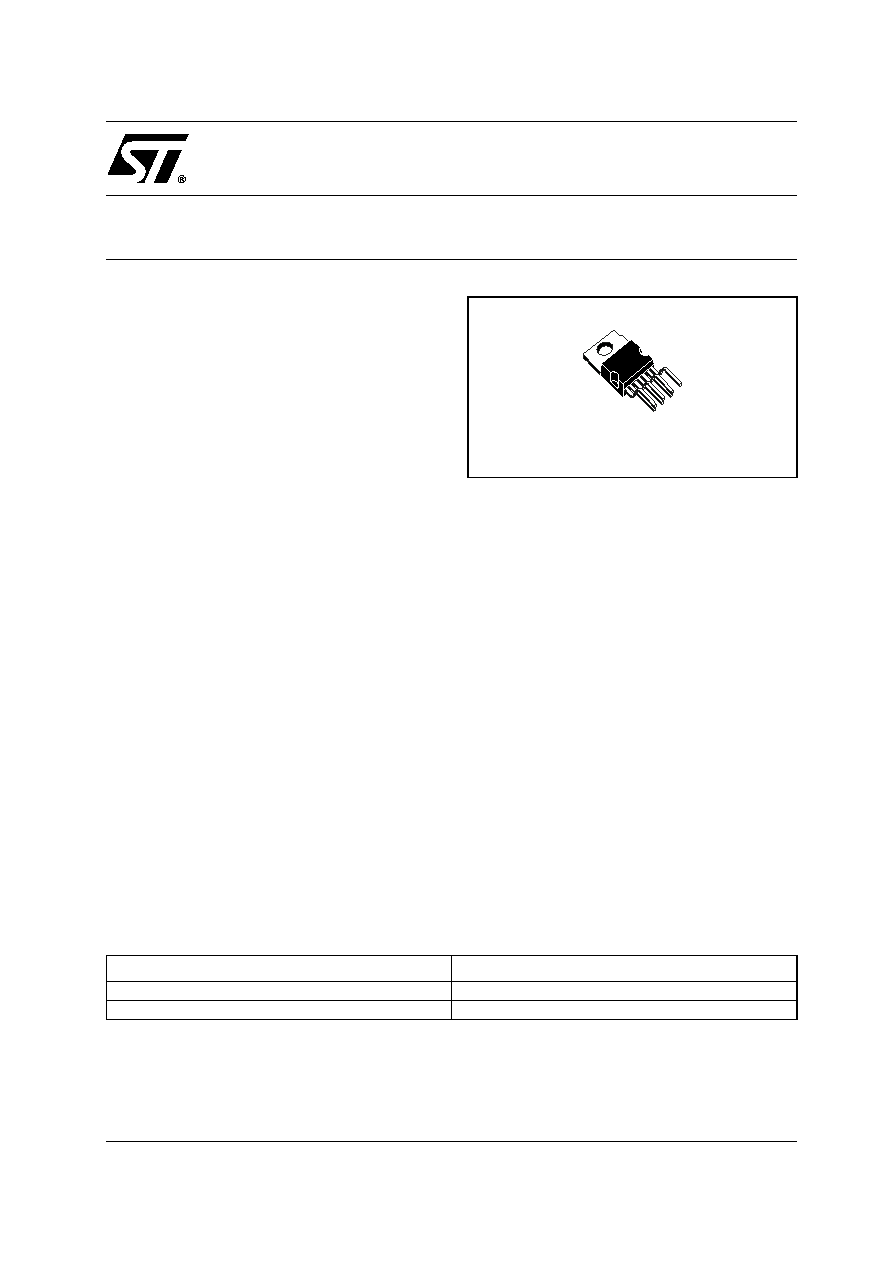
AVAILABLE IN THRU-HOLE PACKAGE
DESCRIPTION
Intended for analog and digital satellite receivers,
the LNBP is a monolithic linear voltage regulator,
assembled in Heptawatt
TM
, specifically designed
to provide the powering voltages and the
interfacing signals to the LNB down-converter.
The regulator output can be logic controlled to be
13V or 18V (typ.) by mean of the V
SEL
pin for the
remote controlling of the LNB. In order to reduce
the power dissipation of the device when the
lowest output voltage is selected, the regulator
has 2 supply inputs (V
CC1
and V
CC2
). They must
be powered respectively at 15V (min.) and 22V
(min.), and an internal switch will automatically
select the appropriate supply voltage according to
the selected output voltage.
The TONE pin (only for the LNBP9 version)
activates the internal oscillator so that the DC
output is modulated by a 22KHz square wave.
This internal oscillator is factory trimmed within a
tolerance of +/- 2KHz, thus no further adjustment
or external components are required.
A burst coding of the 22KHz tone can be
accomplished thanks to the fast response of the
TONE input and the prompt oscillator start-up.
This helps designers which want to implement the
DiSEqC
TM
protocols.
In order to improve design flexibility and to allow
implementation of other LNB remote control
standards, an analogic modulation input pin
(EXTM) is available (LNBP8 version only). An
appropriate DC blocking capacitor must be used
to couple the modulating signal source to the
EXTM pin.
Both versions integrate thermal and short circuit
protection.
The device is packaged in Heptawatt for an easy
thru-hole mounting. If an adequate Heatsink is
provided and higher power losses are acceptable,
both supply pins can be powered by the same 23V
source without affecting any other circuit
performance.
When the IC is powered and put in Stand-by (EN
pin LOW), the regulator output is disabled and the
IC power consumption is reduced to 300µA typ.
Table 1: Order Codes
TYPE
HEPTAWATT
LNBP8
LNBP8V7V
LNBP9
LNBP9V7V
LNBP8
LNBP9
LNB SUPPLY AND CONTROL VOLTAGE REGULATOR
Heptawatt
Rev. 1
LNBP8 - LNBP9
2/8
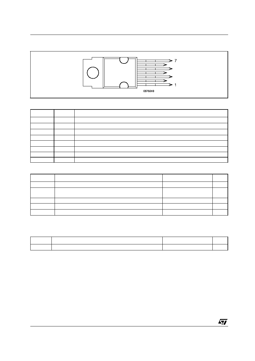
Figure 1: Pin Configuration (top view)
Table 2: Pin Descriptions
Table 3: Absolute Maximum Ratings
Absolute Maximum Ratings are those values beyond which damage to the device may occur. Functional operation under these condition is
not implied.
Table 4: Thermal Data
PIN N∞
NAME
FUNCTION
1
V
CC1
Supply Input 1: 15V to 25V supply. It is automatically selected when V
O
= 13V
2
V
CC2
Supply Input 2: 22V to 25V supply. It is automatically selected when V
O
= 18V
3
OUTPUT
Regulator output. It is 13V typ. when V
SEL
LOW and 18V typ. when V
SEL
HIGH
4
GND
GROUND
5
V
SEL
Output Voltage Selection: Logic Control Input; if LOW V
O
= 13V, when HIGH V
O
= 18V
6
ENABLE
Logic Control Input; force LOW to put the IC in shutdown
7 (LNBP9)
TONE
Logic Control Input; force HIGH to activate the internal 22KHz tone
7 (LNBP8)
EXTM
External Modulation: Needs DC decoupling to the AC source. If not used can be left floating
Symbol
Parameter
Value
Unit
V
CC1,
V
CC2
Input Voltage
-0.3 to 28
V
ENABLE,
TONE, V
SEL
Logic Input Voltage
-0.3 to 7
V
OUTPUT
Output Voltage
28
V
T
J
Operating Junction Temperature Range
-40 to 125
∞C
T
STG
Storage Temperature Range
-55 to 150
∞C
Symbol
Parameter
Value
Unit
R
THJ-C
Thermal Resistance Junction-case
2
∞C/W
LNBP8 - LNBP9
3/8
Figure 2: Block Diagram
Table 5: Electrical Characteristics (V
CC1
= 16V, V
CC2
= 22V, C
I1
= C
I2
= 0.22
µ
F, C
O
=0.1
µ
F,
ENABLE = H, TONE = L (LNBP9), EXTM floating (LNBP8), I
O
= 50mA, T
J
= 0 to 85∞C unless otherwise
specified.)
Symbol
Parameter
Test Conditions
Min.
Typ.
Max.
Unit
V
CC1
V
CC
Supply Input 1
I
O
= 500 mA, TONE = H, V
SEL
= L
15
25
V
V
CC2
V
CC
Supply Input 2
I
O
= 500 mA, TONE = H, V
SEL
= H
22
25
V
V
O
Output Voltage
I
O
= 500 mA, V
SEL
= L
12.5
13
13.5
V
I
O
= 500 mA, V
SEL
= H
17.3
18
18.7
V
V
O
Line Regulation
V
CC1
= 15 to 18V, V
SEL
= L
4
40
mV
V
CC2
= 22 to 25V, V
SEL
= H
4
40
V
O
Load Regulation
V
CC1
= V
CC2
= 22V, I
O
= 50 to 500mA
V
SEL
= L or H
80
180
mV
I
MAX
Output Current Limiting
500
800
mA
f
TONE
Tone Frequency
LNBP9 version, TONE = H
20
22
24
KHz
A
TONE
Tone Amplitude
LNBP9 version, TONE = H
0.55
0.72
0.9
V
D
TONE
Tone Duty Cycle
LNBP9 version, TONE = H
40
50
60
%
t
r
, t
f
Tone Rise and Fall Time
LNBP9 version, TONE = H
5
10
15
µ
s
G
EXTM
External Modulation Gain
LNBP8 version,
V
O
/
V
EXTM
,
f = 10Hz to 40KHz
5
V
EXTM
External Modulation Input
Voltage
LNBP8 version, AC Coupling
400
mV
Z
EXTM
External Modulation
Impedance
LNBP8 version, f = 10Hz to 40KHz
400
V
IL
Control Input Logic LOW
ENABLE, TONE (LNBP9 version), V
SEL
0.8
V
V
IH
Control Input Logic HIGH
ENABLE, TONE (LNBP9 version), V
SEL
2.5
V
I
IH
Control Pins Input Current
V
IH
= 5V, ENABLE, TONE (LNBP9
version), V
SEL
20
µ
A
I
CC
Supply Current
Output Disabled (ENABLE = L)
0.3
1
mA
Output Enabled (ENABLE = H), TONE = H
I
O
= 500mA
3
6
mA
T
SHDN
Temperature Shutdown
150
∞C
LNBP8 - LNBP9
4/8
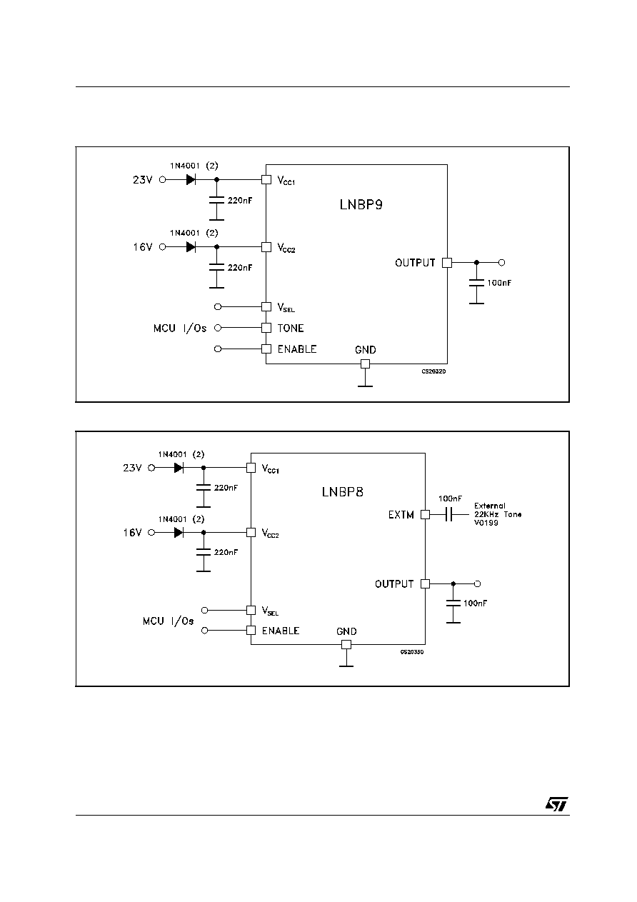
TYPICAL APPLICATION CIRCUITS
Figure 3: LNBP9 with 22KHz Tone Control Pin
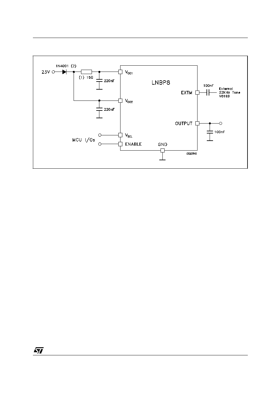
Figure 4: LNBP8 with external 22KHz Input Pin (EXTM)
LNBP8 - LNBP9
5/8
Figure 5: Single Supply Solution
(1) In a single supply configuration the presence of the input resistor in the 12-15
range is suggested
only to reduce the device power dissipation during the 13V output condition. The resistor can be omitted
in spite of power dissipation increase.
(2) The input diodes are mandatory to protect the device from any reverse current.