 | –≠–ª–µ–∫—Ç—Ä–æ–Ω–Ω—ã–π –∫–æ–º–ø–æ–Ω–µ–Ω—Ç: LPR30D | –°–∫–∞—á–∞—Ç—å:  PDF PDF  ZIP ZIP |
LPR30
LOW DROP VOLTAGE REGULATOR DRIVE
FOR EXTERNAL N-CHANNEL POWER MOSFET
Æ
May 2000
s
VERY LOW DROPOUT POWER MOSFET
DRIVER
s
HIGH PRECISION Vref = 2.5V (
±
2%)
s
VERY LOW CURRENT DRAIN (TYP. 2mA)
s
REFERENCE OUTPUT CURRENT UP TO
20mA
s
OPERATING SUPPLY VOLTAGE FROM 5V
TO 30V
s
MAXIMUM INPUT VOLTAGE ON-GATE PIN
(N. 8) UP TO 60V
s
INTERNAL CURRENT LIMIT OPERATIONAL
AMPLIFIER OFFSET TRIMMED AT
50mV
±
10mV
s
NO CAPACITOR IS NEEDED FOR STABILITY
OF REFERENCE OUTPUT
s
TEMPERATURE RANGE 0
o
C TO 70
o
C
APPLICATION
s
ULTRA HIGH CURRENT ULTRA LOW
DROPOUT VOLTAGE REGULATOR
s
CONSTANT HIGH CURRENT SOURCE
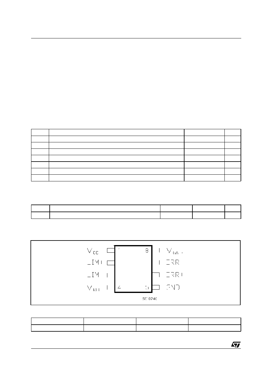
BLOCK DIAGRAM
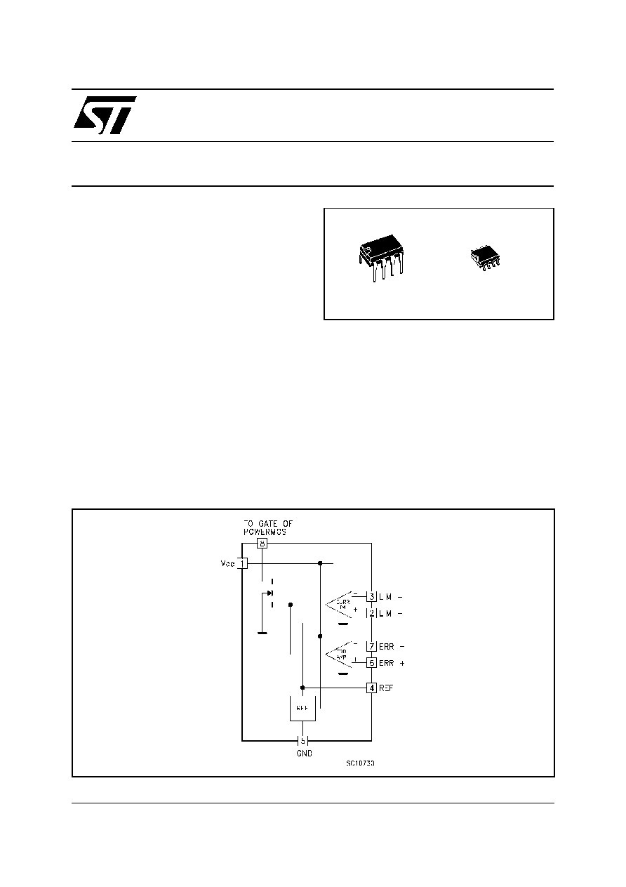
DIP-8
SO-8
s
LOW PARTS COUNT 5V TO 3.3V
COMPUTER SUPPLY
s
LOW NOISE/LOW DROP SMPS POST
REGULATOR
DESCRIPTION
The LPR30 is a very Low Dropout Regulator
Controller in a single IC solution for very high
current low dropout linear voltgage regulator. It
uses an external N-CHANNEL POWER MOSFET
as the linear pass element. The LPR30 features a
dropout voltage as low as the R
DS(on)
of the
1/10
external Power MOSFET multiplied by the output
current. Consequently the output current can be
as high as the POWER MOSFET can provide
(also using an adeguate heatsink).
The V
CC
of the LPR30 range from 5V to 30V. For
very low drop voltage operation,the LPR30
requires an external gate drive supply to provide
the control voltage needed to drive the gate of the
external POWER MOSFET.
The regulator output is constant-current limited
when the controller detects 50mV across an
external sense resistor.
It has an internal high precision (
±
2%) Voltage
Reference at 2.5V
The output regulated voltage is possible to
program to any voltage from 1V to more than
50V.
Flexible design is achieved by the availability of
the
Voltage
Reference Output
through
an
external pin (N.4) that is able to supply more than
20mA as load current. The LPR30 is available in
8 pin plastic DIP and in SO-8 for SMD. In both
package versions it is able to operate from 0
o
C to
70
o
C.
ABSOLUTE MAXIMUM RATINGS
Symbol
Parameter
Value
Unit
V
CC
DC Input Voltage
36
V
I
oREF
Reference Output Current
Internally Limited
P
tot
Power Dissipation
1
W
T
op
Operating Junction Temperature Range
0 to 70
o
C
T
st g
Storage Temperature Range
- 40 to 150
o
C
V
gate
Maximum Gate Voltage (pin n8)
60
V
I
gate
Maximum Gate Current (pin n8)
200
mA
Absolute Maximum Ratings are those values beyond which damage to the device may occur.
Functional operation under these conditions is not implied.
THERMAL DATA
Symbol
Parameter
DIP-8
SO-8
Unit
R
thj- amb
Thermal Resistance Junction-ambient (*)
Max
130 to 180
100 to 150
o
C/W
(*) This value depends from thermal design of PCB on which the device is mounted.
CONNECTION DIAGRAM (top view)
ORDERING NUMBERS
Type
DIP-8
SO-8
SO-8 (tape & reel)
LPR30
LPR30N
LPR30D
LPR30D-TR
LPR30
2/10
ELECTRICAL CHARACTERISTICS
(Refer to the test circuits, V
CC
= 10V, T
j
= 25
o
C unless otherwise specified.
GENERAL
Symbol
Parameter
Test Conditions
Min.
Typ.
Max.
Unit
V
CC
Operating Supply Voltage
5
30
V
I
CC
Supply Current
I
K
= 0
µ
A
V
CC
= 30 V
T
j
= 0 to 70
o
C
ERR(-), LIM(-) = 1V
ERR(+), LIM(+) = 0V
2
4
mA
V
OSAT
Output Saturation Voltage
V
CC
= 5 V
I
O
= 100 mA
T
j
= 0 to 70
o
C
ERR(-), LIM(-) = 1V
ERR(+), LIM(+) = 0V
280
500
mV
I
OLK
Output Leakage Current
V
CC
= 5 V
V
O
= 60 V
ERR(-), LIM(-) = 0V
ERR(+), LIM(+) = 1V
100
µ
A
REFERENCE BLOCK
Symbol
Parameter
Test Conditions
Min.
Typ.
Max.
Unit
V
REF
Reference Output Voltage
2.45
2. 5
2.55
V
I
K
Reference Output Current
20
mA
V
REF
/
I
K
Reference Output Voltage
Change
I
K
= 1 to 20 mA C
REF
= 0 pF
3
mV
SVR
Supply Voltage Rejection
V
IN
< 10 V
±
1V f = 120 Hz C
REF
= 0 pF
70
dB
eN
Output Noise
B = 10 Hz to 10 KHz
I
K
= 10 mA C
REF
= 0 pF
50
µ
V
ERROR AMPLIFIER BLOCK
Symbol
Parameter
Test Conditions
Min.
Typ.
Max.
Unit
I
B
Input Bias Current
0. 3
1
µ
A
V
OS
Input OffsetVoltage
V
CC
= 5 to 30 V
T
j
= 0 to 70
o
C
5
mV
I
OS
Input OffsetCurrent
5
50
nA
G
V
Open Loop Gain
T
j
= 0 to 70
o
C
80
dB
V
CM
Input Common Mode Voltage
Range
T
j
= 0 to 70
o
C
1
V
CC
-1
V
CMR
Common Mode Rejection
70
dB
SVR
Supply Voltage Rejection
V
IN
= 9 to 11V
f = 120Hz
V
IN
= 9 to 11V
f = 10KHz
70
60
dB
dB
CURRENT LIMITING BLOCK
Symbol
Parameter
Test Conditions
Min.
Typ.
Max.
Unit
I
B
Input Bias Current
0. 5
µ
A
V
OS
Input OffsetVoltage
T
j
= 0 to 70
o
C
40
60
V
G
V
Open Loop Gain
T
j
= 0 to 70
o
C
50
dB
V
CM
Input Common Mode Voltage
Range
T
j
= 0 to 70
o
C
0
V
CC
-3
V
LPR30
3/10
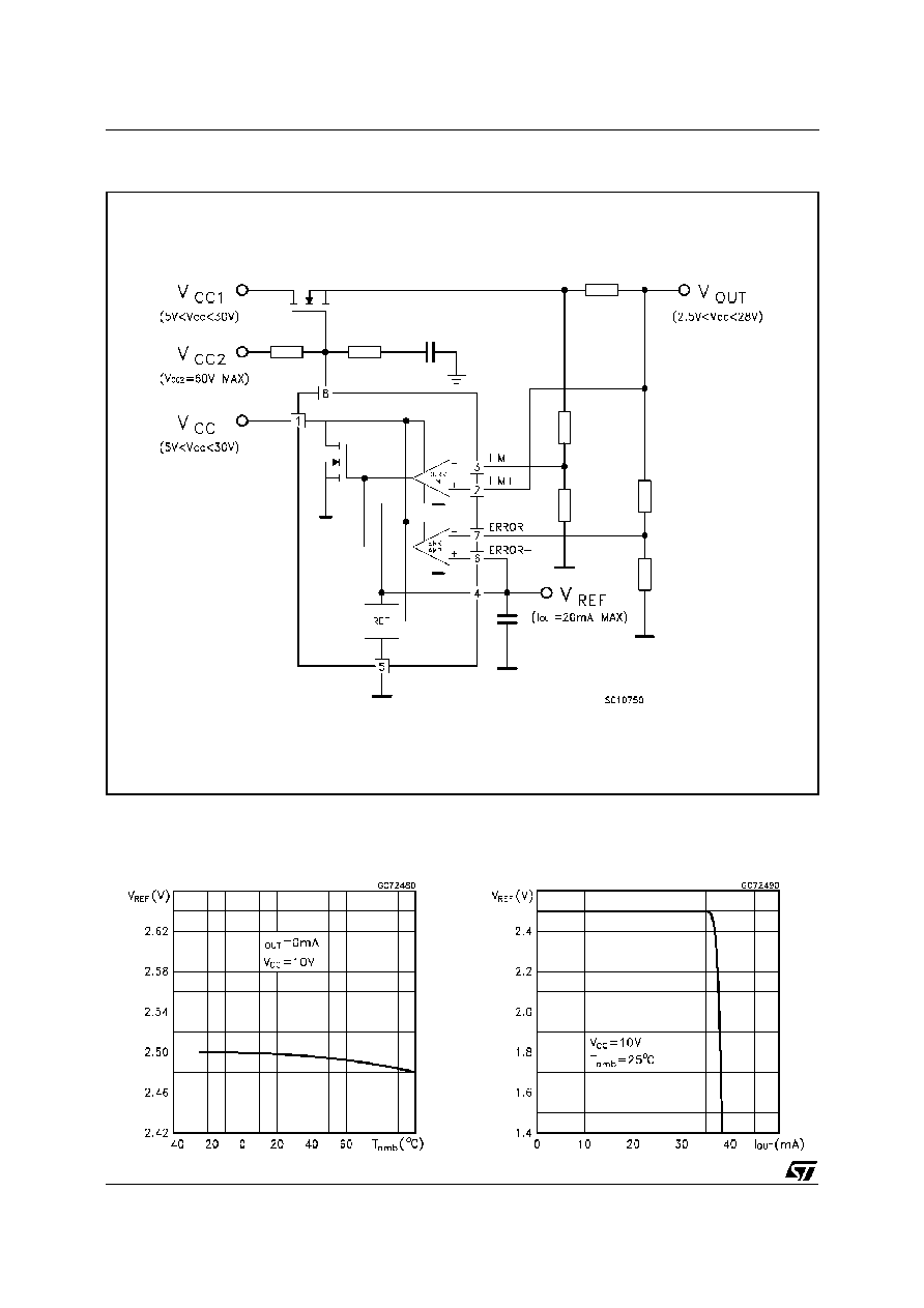
TEST CIRCUIT
Reference Output Voltage vs Temperature
Reference Output Voltage vs Load Current
TYPICAL PERFORMANCE CHARACTERISTICS
LPR30
4/10
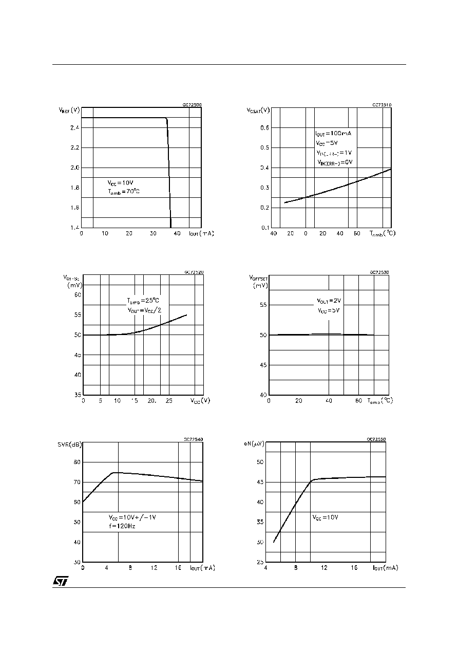
Reference Output Voltage vs Load Current
Current Limit Input Offset Voltage vs Supply
Voltage
Reference Supply Voltage Rejection vs Output
Current
Error Amplifier Output Saturation Voltage vs
Temperature
Current Limit Input Offset Voltage vs Supply
Voltage
Reference Output Noise vs Output Current
LPR30
5/10
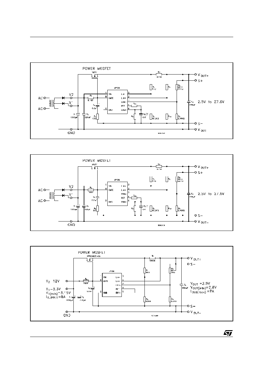
APPLICATION INFORMATION
Figure 1: LPR30 Typical Application
Figure 2: Configuration For Faster Response
Figure 3: Configuration For V
IN
= 3.3V, V
OUT
= 2.9V, I
OUT
= 7A
(*) This capacitor improves noise performance; can be omitted in most applications
LPR30
6/10
APPLICATION INFORMATION (contiued)
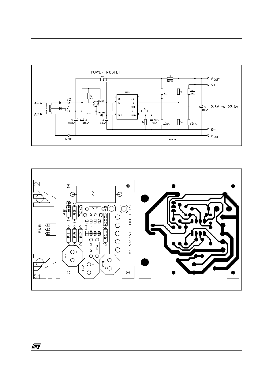
Figure 4: Application For Very Fast Responce Speed
STANDARD APPLICATION DEMOBOARD
(*) This capacitor improves noise performance; can be omitted in most applications
Note: This demoboard refers to the typical application shown in figure 1
LPR30
7/10
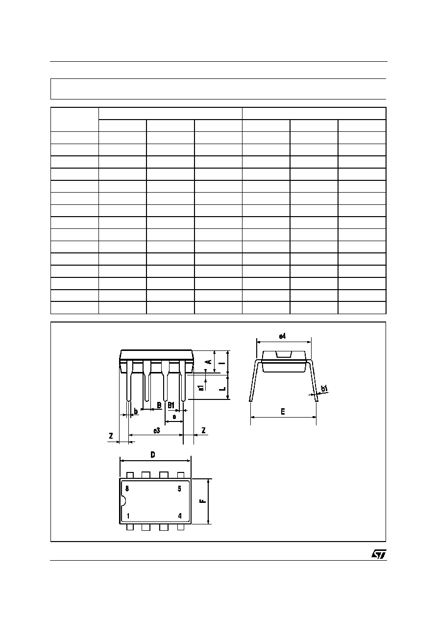
DIM.
mm
inch
MIN.
TYP.
MAX.
MIN.
TYP.
MAX.
A
3.3
0.130
a1
0.7
0.028
B
1.39
1.65
0.055
0.065
B1
0.91
1.04
0.036
0.041
b
0.5
0.020
b1
0.38
0.5
0.015
0.020
D
9.8
0.386
E
8.8
0.346
e
2.54
0.100
e3
7.62
0.300
e4
7.62
0.300
F
7.1
0.280
I
4.8
0.189
L
3.3
0.130
Z
0.44
1.6
0.017
0.063
P001F
Plastic DIP-8 MECHANICAL DATA
LPR30
8/10
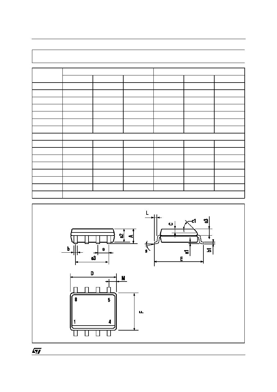
DIM.
mm
inch
MIN.
TYP.
MAX.
MIN.
TYP.
MAX.
A
1.75
0.068
a1
0.1
0.25
0.003
0.009
a2
1.65
0.064
a3
0.65
0.85
0.025
0.033
b
0.35
0.48
0.013
0.018
b1
0.19
0.25
0.007
0.010
C
0.25
0.5
0.010
0.019
c1
45 (typ.)
D
4.8
5.0
0.188
0.196
E
5.8
6.2
0.228
0.244
e
1.27
0.050
e3
3.81
0.150
F
3.8
4.0
0.14
0.157
L
0.4
1.27
0.015
0.050
M
0.6
0.023
S
8 (max.)
0016023
SO-8 MECHANICAL DATA
LPR30
9/10

Information furnished is believed to be accurate and reliable. However, STMicroelectronics assumes no responsibility for the consequences
of use of such information nor for any infringement of patents or other rights of third parties which may result from its use. No license is
granted by implication or otherwise under any patent or patent rights of STMi croelectronics. Specification mentioned in this publication are
subject to change without notice. This publication supersedes and replaces all information previously supplied. STMi croelectronics products
are not authorized for use as critical components in life support devices or systems withoutexpress written approval of STMicroelectronics.
The ST logo is a registered trademark of STMicroelectronics
©
2000 STMicroelectronics ≠ Printed in Italy ≠ All Rights Reserved
STMicroelectronics GROUP OF COMPANIES
Australia - Brazil - China - Finland - France - Germany - Hong Kong - India - Italy - Japan - Malaysia - Malta - Morocco
Singapore - Spain - Sweden - Switzerland - United Kingdom - U.S.A.
http://www.st.com
.
LPR30
10/10