 | –≠–ª–µ–∫—Ç—Ä–æ–Ω–Ω—ã–π –∫–æ–º–ø–æ–Ω–µ–Ω—Ç: LRI512 | –°–∫–∞—á–∞—Ç—å:  PDF PDF  ZIP ZIP |
1/54
July 2002
LRI512
Memory TAG IC 512 bit High Endurance EEPROM
13.56MHz, ISO 15693 Standard Compliant with E.A.S.
FEATURES SUMMARY
s
ISO15693 Standard: Fully Compliant
s
13.56 MHz ±7 kHz Carrier Frequency
s
To the LRI512:
10% or 100% ASK modulation using:
≠ 1/4 pulse position coding (26 kbit/s)
≠ 1/256 pulse position coding (1.6 kbit/s)
s
From the LRI512:
Load modulation using Manchester coding with
423 kHz and 484 kHz subcarrier in:
≠ Fast data rate (26 kbit/s)
≠ Low data rate (6.6 kbit/s)
s
Internal Tuning Capacitor
s
512 bits EEPROM with Block Lock Feature
s
64-bit Unique Identifier (UID)
s
EAS features
s
READ block and WRITE block (32-bit blocks)
s
5 ms Programming Time (typical)
s
More than 100,000 Erase/Write Cycles
s
More than 40 Year Data Retention
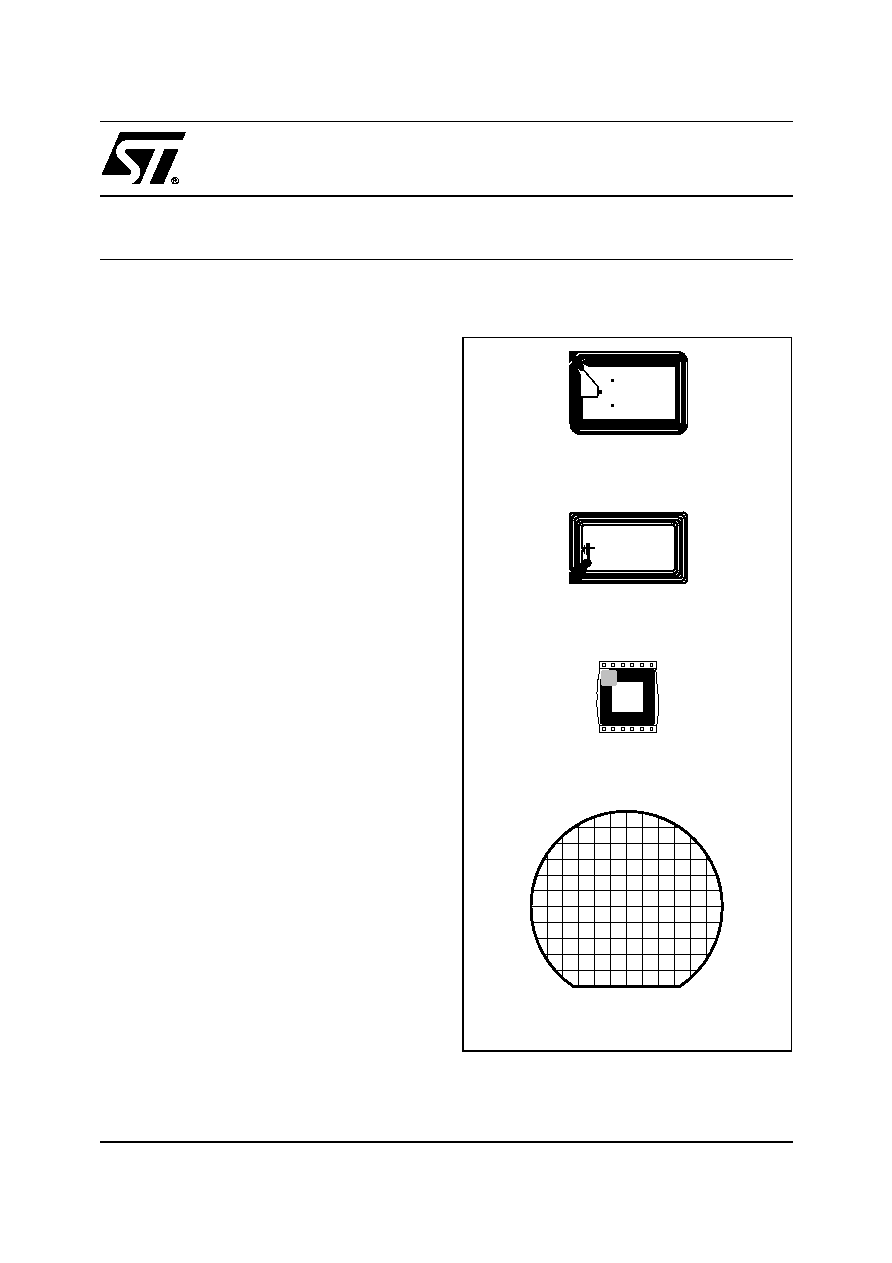
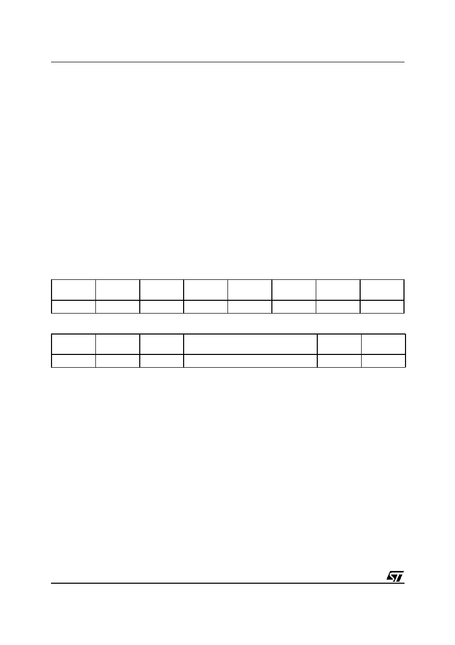
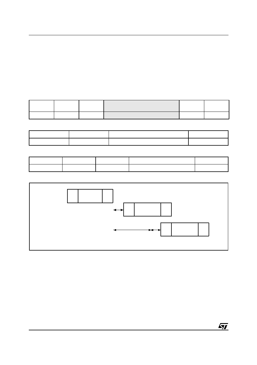
Figure 1. Delivery Forms
Wafer
Antenna
(A1T/ISOR, A1S/ISOR)
Antenna
(C40)
Antenna
(A2T/ISOK)
LRI512
2/54
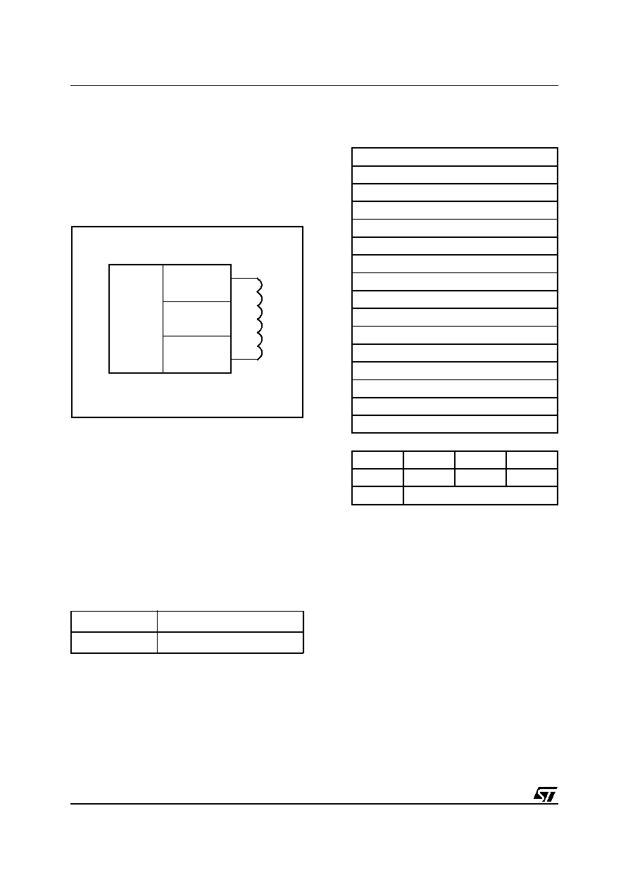
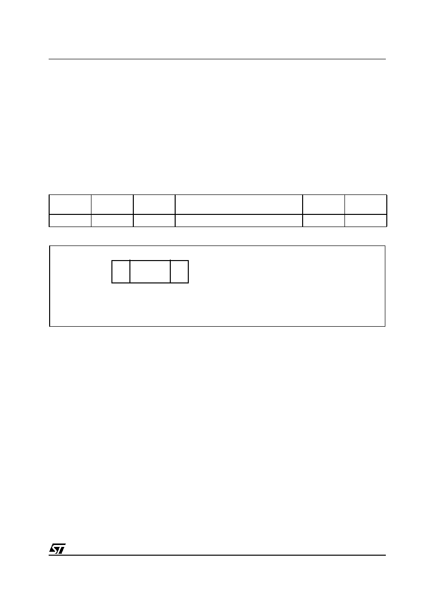
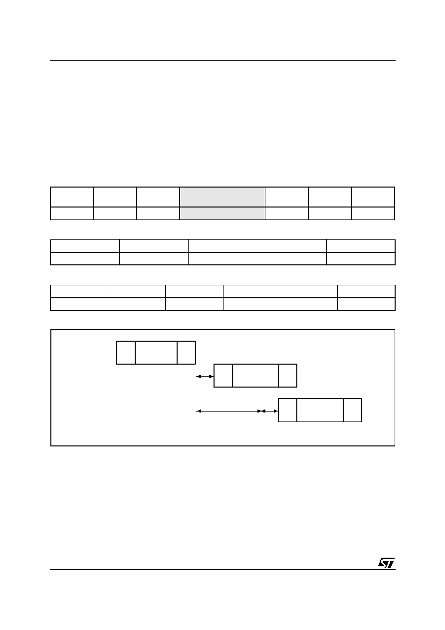
SUMMARY DESCRIPTION
The LRI512 is a contactless memory, powered by
an externally transmitted radio wave. It is fully
compliant with the ISO15693 recommendation for
radio-frequency power and signal interface.
The LRI512 contains 512 bits of Electrically
Erasable Programmable Memory (EEPROM). The
memory is organized as 16 blocks of 32 bits.
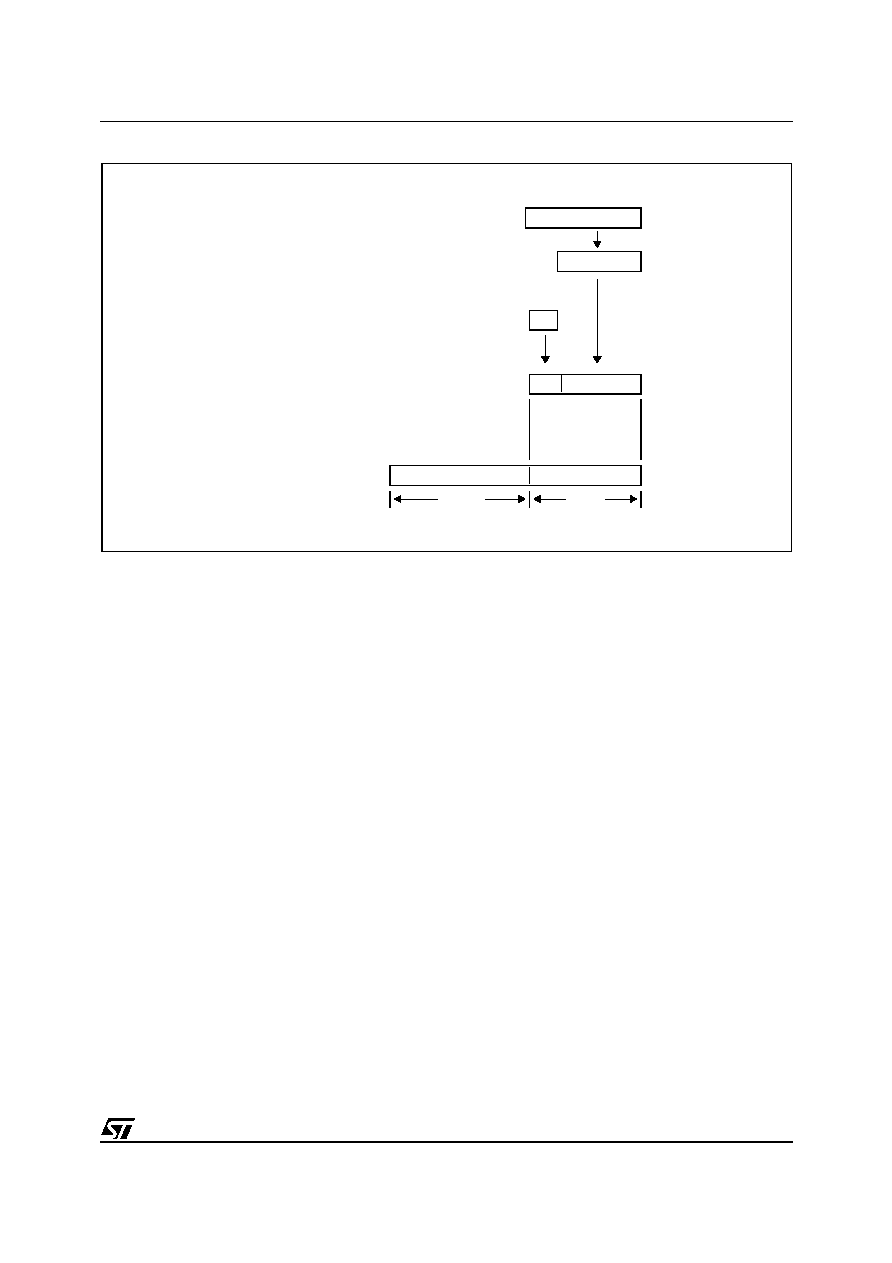
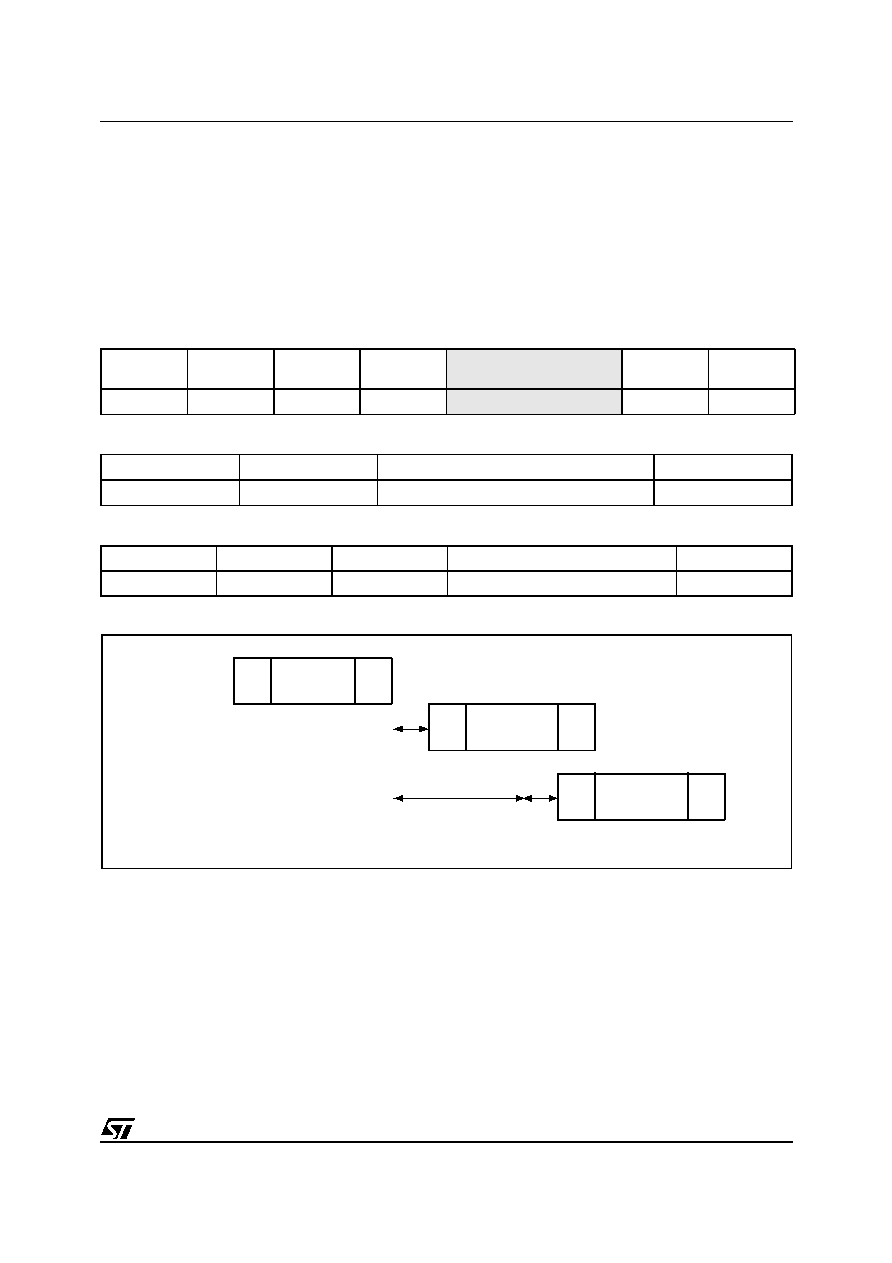
Figure 2. Logic Diagram
The LRI512 is accessed by modulating the
13.56 MHz carrier frequency. Incoming data are
demodulated from the received signal amplitude
modulation (ASK, Amplitude Shift Keying). The
received ASK wave is 10% or 100% modulated
(amplitude modulation). The Data transfer rate is
1.6 kbit/s using the 1/256 pulse coding mode and
26 kbit/s using the 1/4 pulse coding modes.
Outgoing data are generated by antenna load
variation, using the Manchester coding, using one
or two sub-carrier frequencies at 423 kHz and
484 kHz. The Data transfer rate is 6.6 kbit/s, in the
low data rate mode, and 26 kbit/s, in the fast data
rate mode.
Table 1. Signal Names
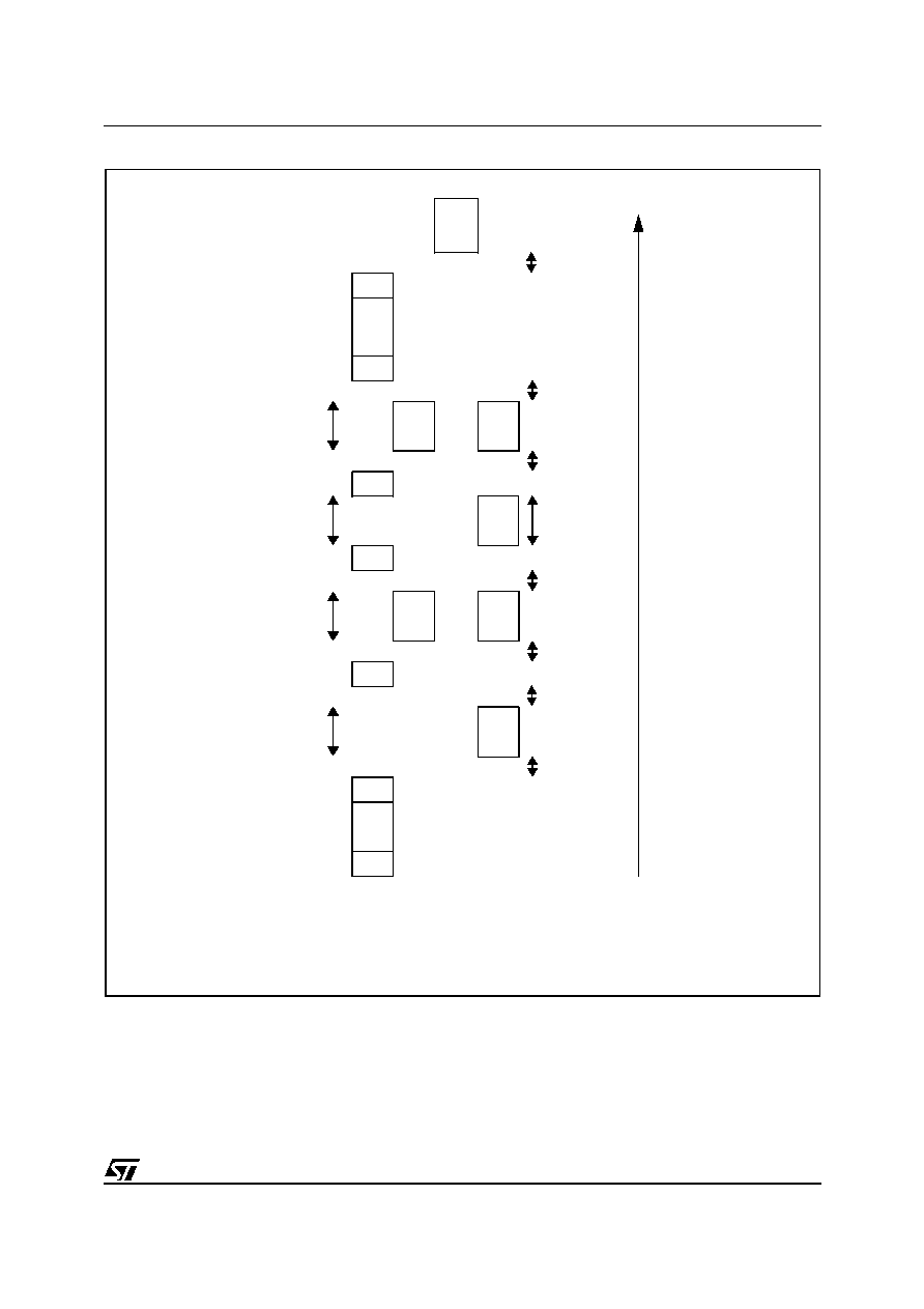
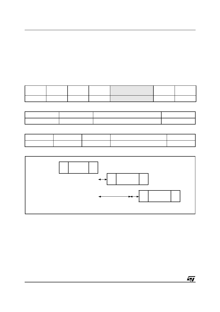
Memory Mapping
The LRI512 is divided in 16 blocks of 32 bits. Each
block can be individually Write Protected using a
specific Lock command.
Table 2. LRI512 Memory Map
The User Area consists of blocks that are always
accessible in READ. WRITE commands are pos-
sible if the addressed block is not locked. During a
WRITE, the 32 bits of the block are replaced by the
new 32-bit value.
The LRI512 also has a 64-bit block that is used to
store the 64-bit Unique Identifier (UID). This UID is
compliant to the ISO15963 description, and its val-
ue is used during the anti-collision sequence (IN-
VENTORY). This block is not accessible by the
user, and the value is written by ST on the produc-
tion line.
The LRI512 also has an AFI register in which the
Application Family Identifier is stored, for use in
the anti-collision algorithm.
AC1
Antenna Coil
AC0
Antenna Coil
AI04008B
AC1
LRI512
AC0
Power
Supply
Regulator
Manchester
Load
Modulator
ASK
Demodulator
512 bit
EEPROM
Addr 0
7
8
15
16
23
24
31
0
User Area
1
User Area
2
User Area
3
User Area
4
User Area
5
User Area
6
User Area
7
User Area
8
User Area
9
User Area
10
User Area
11
User Area
12
User Area
13
User Area
14
User Area
15
User Area
UID 0
UID 1
UID 2
UID 3
UID 4
UID 5
UID 6
UID 7
AFI

3/54
LRI512
Commands
The LRI512 supports the following commands:
≠
INVENTORY
: used to perform the anti-collision
sequence.
≠
STAY QUIET:
to put the LRI512 in quiet mode.
The LRI512 is then deselected and does not re-
spond to any command.
≠
SELECT:
used to select the LRI512. After this
command, the LRI512 processes all READ/
WRITE commands with the Select_Flag set.
≠
RESET TO READY:
to put the LRI512 in the
ready state.
≠
READ BLOCK:
to output the 32 bits of the se-
lected block and its locking status.
≠
WRITE BLOCK:
to write the 32-bit value in the
selected block, provided that it is not locked.
≠
LOCK BLOCK:
to lock the selected block. After
this command, the block cannot be modified.
≠
WRITE AFI:
to write the 8-bit value in the AFI
register, provided that it is not locked.
≠
LOCK AFI:
to lock the AFI register.
≠
ACTIVATE EAS:
to set the non volatile EAS bit.
When the EAS bit is set, the LRI512 answers to
the POOL EAS command.
≠
DEACTIVATE EAS:
to reset the non volatile
EAS bit, so that the LRI512 no longer answers
to the POOL EAS command.
≠
POOL EAS
: used to request all LRI512s in the
Reader field to generate the EAS signal, provid-
ed that their EAS bit is set.
Initial Dialogue for Vicinity Cards
The dialogue between the Vicinity Coupling De-
vice (VCD) and the Vicinity Integrated Circuit Card
(LRI512) is conducted through the following con-
secutive operations:
≠ activation of the LRI512 by the RF operating
field of the VCD.
≠ transmission of a command by the VCD.
≠ transmission of a response by the LRI512.
These operations use the RF power transfer and
communication signal interface specified in the fol-
lowing paragraphs. This technique is called Read-
er Talk First (RTF).
Power Transfer
Power transfer to the LRI512 is accomplished by
radio frequency at 13.56 MHz via coupling anten-
nas in the LRI512 and in the VCD. The RF operat-
ing field of the VCD is transformed on the LRI512
antenna as an AC voltage which is re-dressed, fil-
tered and internally regulated. The amplitude
modulation (ASK) on this received signal is de-
modulated by the ASK demodulator.
Frequency
The ISO15693 standard defines the carrier fre-
quency (
f
c
) of the operating field to be
13.56 MHz ± 7 kHz.
Operating Field
The LRI512 operates continuously between H
min
and H
max
.
≠ The minimum operating field is H
min
and has a
value of 150 mA/m rms.
≠ The maximum operating field is H
max
and has a
value of 5 A/m rms.
A VCD shall generate a field of at least H
min
and
not exceeding H
max
in the operating volume.
LRI512
4/54
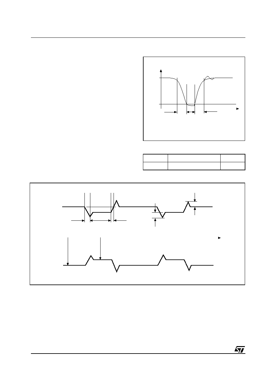
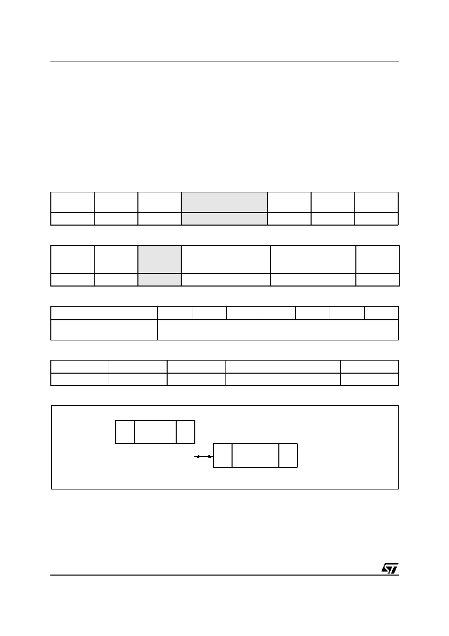
COMMUNICATION SIGNAL FROM VCD TO LRI512
Since the LRI512 is fully compliant with the
ISO15693 recommendation, the descriptions and
illustrations that follow are very heavily based on
those of the ISO/IEC documents: ISO/IEC 15693-
2:2000(E) and ISO/IEC 15693-3:2001(E). This
has been done with the kind permission of the ISO
Copyright Office.
Communications between the VCD and the
LRI512 takes place using the modulation principle
of ASK (amplitude modulation). Two modulation
indices are used, 10% and 100%. The LRI512 de-
codes both. The VCD determines which index is
used.
The modulation index is defined as [a-b]/[a+b]
where a and b are the peak and minimum signal
amplitude, respectively, of the carrier frequency.
Depending of the choice made by the VCD, a
"pause" will be created as described in Figure 3
and Figure 4.
The LRI512 is operational for any degree of mod-
ulation index from between 10% and 30%.
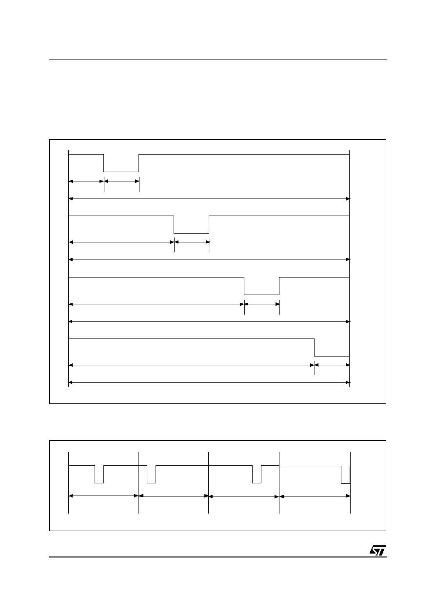
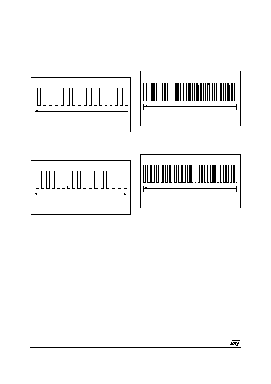
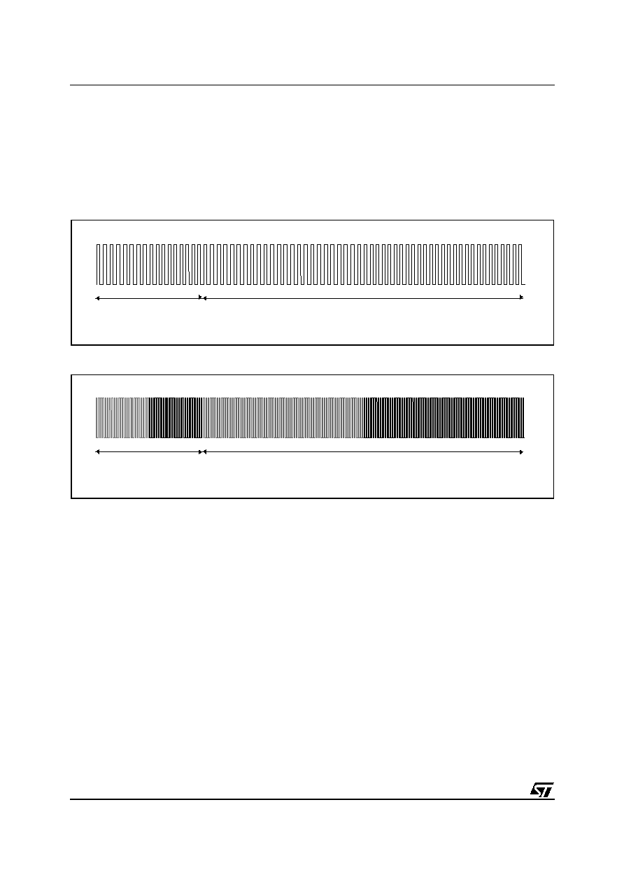
Figure 3. 100% Modulation Waveform
Table 3. 10% Modulation Parameters
Figure 4. 10% Modulation Waveform
hr
0.1 x (a-b)
max
hf
0.1 x (a-b)
max
AI06683
tRFF
tRFSBL
tRFR
105%
a
t
100%
95%
60%
5%
AI06655
tRFF
tRFSFL
tRFR
hr
hf
a
b
t
5/54
LRI512
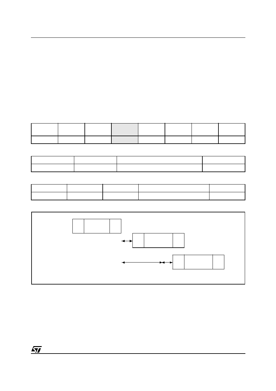
DATA RATE AND DATA CODING
The data coding implemented in the LRI512 uses
pulse position modulation. Both data coding
modes that are described in the ISO15693 are
supported by the LRI512. The selection is made
by the VCD and indicated to the LRI512 within the
Start of Frame (SOF).
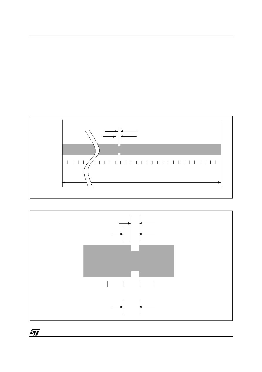
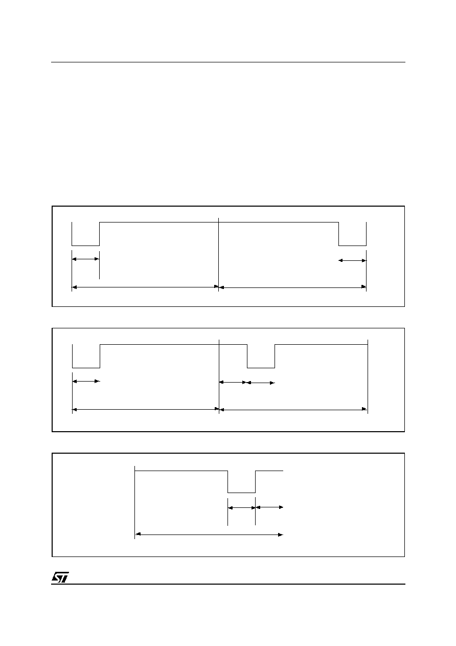
Data Coding Mode: 1 Out of 256
The value of one single byte is represented by the
position of one pause. The position of the pause
on 1 of 256 successive time periods of 18.88 µs
(256/f
C
), determines the value of the byte. In this
case the transmission of one byte takes 4.833 ms
and the resulting data rate is 1.65 kbit/s (f
C
/8192).
Figure 5 illustrates this pulse position modulation
technique. In this figure, data E1h (225d) is sent by
the VCD to the LRI512.
The pause shall occur during the second half of
the position of the time period that determines the
value, as shown in Figure 6.
A pause during the first period transmit the data
value 00h. A pause during the last period transmits
the data value FFh (255d).
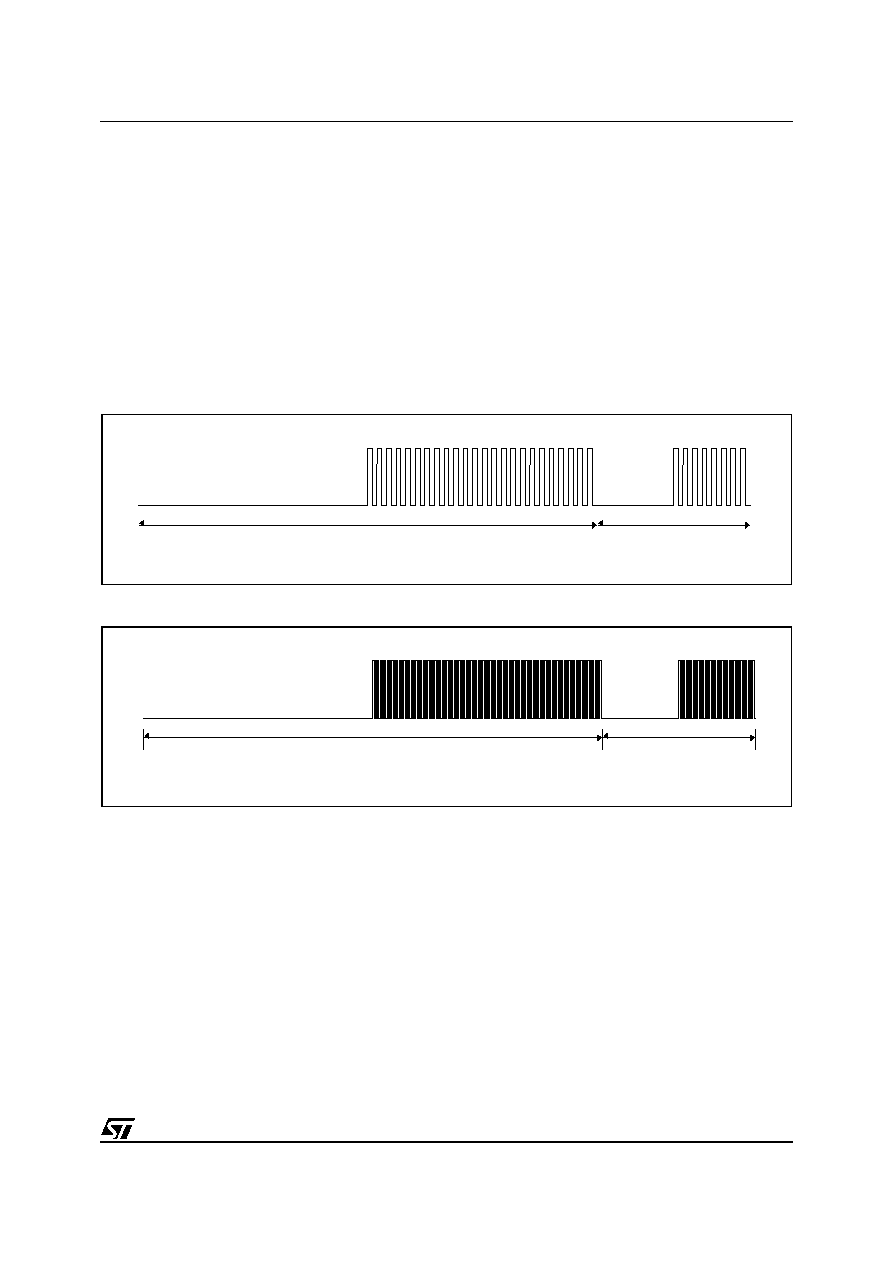
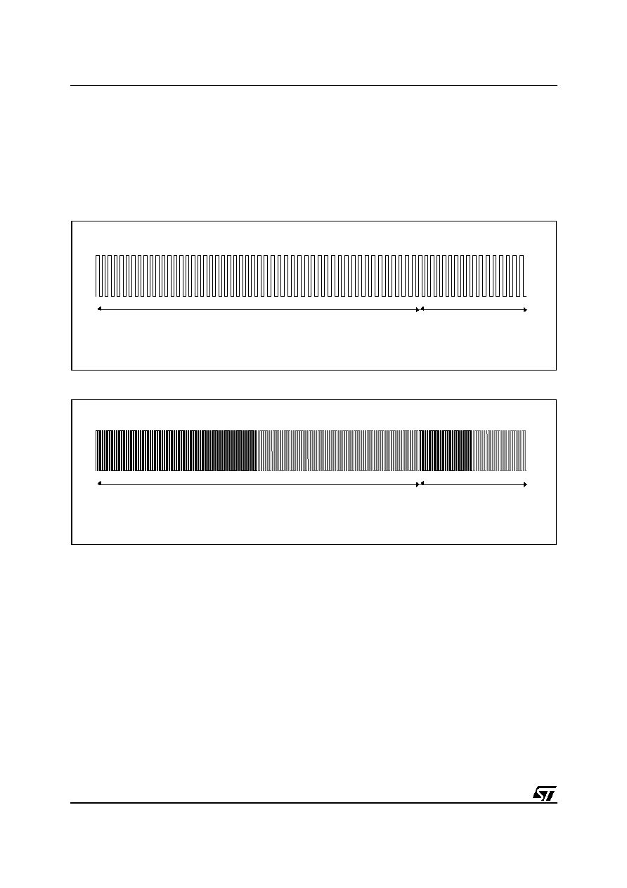
Figure 5. 1 Out of 256 Coding Mode
Figure 6. Detail of One Time Period
AI06656
0 1 2 3 . . . . . . . . 2 . . . . . . . . . . . . . . . . . . . . . 2 2 2 2
. . . . . . . . . 2 . . . . . . . . . . . . . . . . . . . . . 5 5 5 5
. . . . . . . . . 5 . . . . . . . . . . . . . . . . . . . . . 2 3 4 5
4.833 ms
18.88 µs
9.44 µs
Pulse
Modulated
Carrier
AI06657
2
2
5
18.88 µs
9.44 µs
Pulse
Modulated
Carrier
2
2
6
2
2
4
. . . . . . .
. . . . . . .
Time Period
one of 256
LRI512
6/54
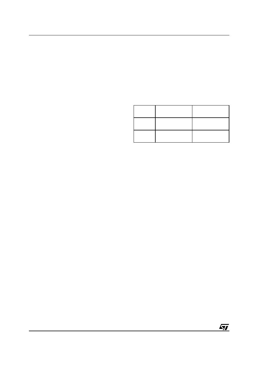
Data Coding Mode: 1 Out of 4
The value of 2 bits is represented by the position
of one pause. The position of the pause on 1 of 4
successive time periods of 18.88 µs (256/f
C
), de-
termines the value of the 2 bits. Four successive
pairs of bits form a byte, where the least significant
pair of bits is transmitted first.
In this case the transmission of one byte takes
302.08 µs and the resulting data rate is 26.48 kbit/
s (f
C
/512). Figure 7 illustrates the 1 out of 4 pulse
position technique and coding.
Figure 7. 1 Out of 4 Coding Mode
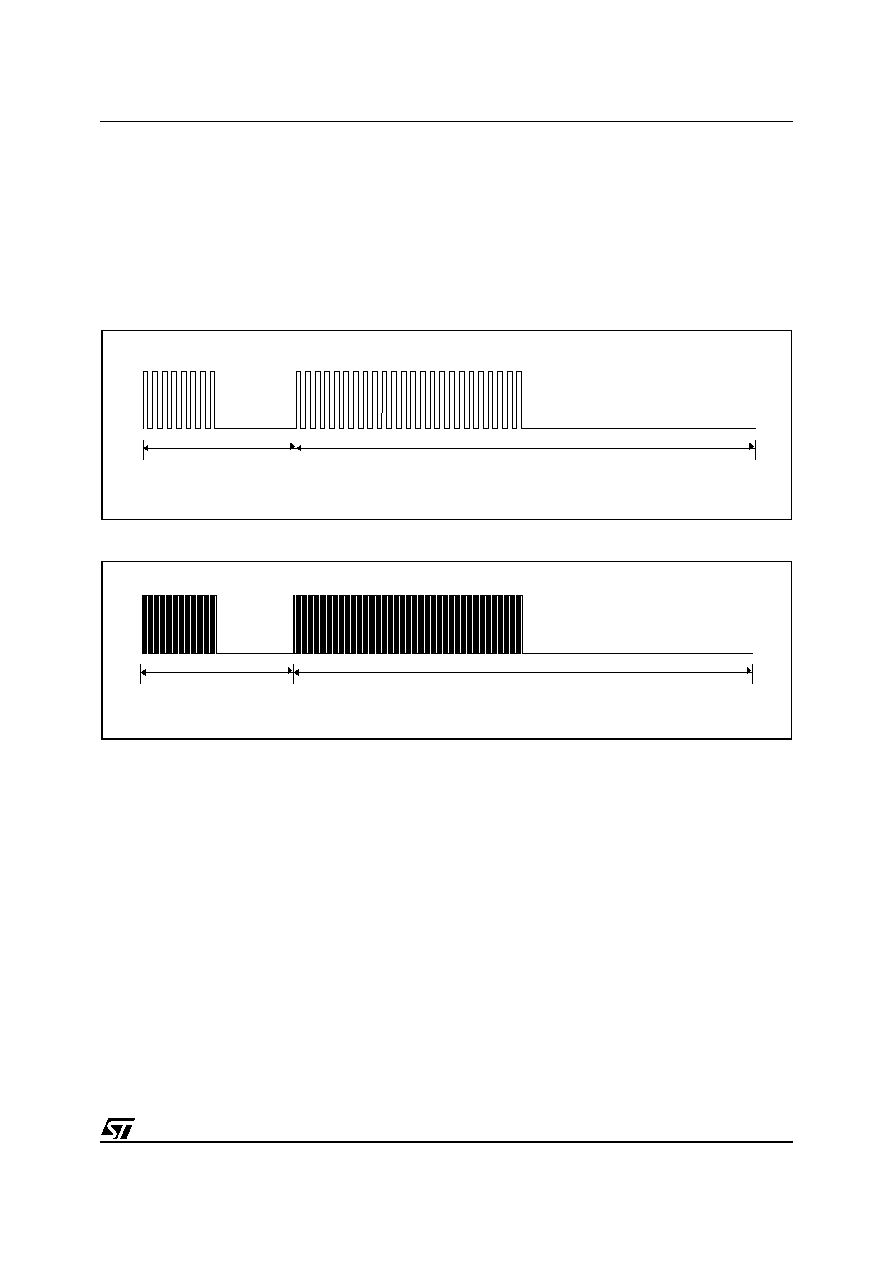
For example Figure 8 shows the transmission of
E1h (225d, 1110 0001b) by the VCD.
Figure 8. 1 Out of 4 Coding Example
AI06658
9.44 µs
9.44 µs
75.52 µs
28.32 µs
9.44 µs
75.52 µs
47.20µs
9.44 µs
75.52 µs
66.08 µs
9.44 µs
75.52 µs
Pulse position for "00"
Pulse position for "11"
Pulse position for "10" (0=LSB)
Pulse position for "01" (1=LSB)
AI06659
75.52 µs
75.52 µs
75.52 µs
75.52 µs
00
10
01
11
7/54
LRI512
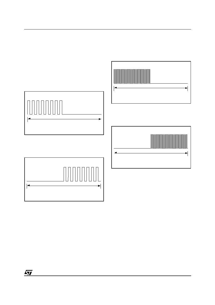
VCD to LRI512 Frames
Frames are delimited by a Start of Frame (SOF)
and an End of Frame (EOF) and are implemented
using code violation. Unused options are reserved
for future use.
The LRI512 is ready to receive a new command
frame from the VCD after a delay of t
2
after having
sent a response frame to the VCD (as specified in
Table 59).
The LRI512 generates a Power-on delay of t
MINCD
after being activated by the powering field (as
specified in Table 59). After this delay, the LRI512
is ready to receive command frames from the
VCD.
Start of Frame (SOF)
The SOF defines the data coding mode the VCD
is to use for the following command frame.
The SOF sequence described in Figure 9 selects
the 1 out of 256 data coding mode.
The SOF sequence described in Figure 10 selects
the 1 out of 4 data coding mode.
The EOF sequence for either coding mode is de-
scribed in Figure 11.
Figure 9. SOF to Select 1 Out of 256 Data Coding Mode
Figure 10. SOF to Select 1 Out of 4 Data Coding Mode
Figure 11. EOF for Either Data Coding Mode
AI06661
37.76 µs
9.44 µs
9.44 µs
37.76 µs
AI06660
37.76 µs
9.44 µs
9.44 µs
37.76 µs
9.44 µs
AI06662
9.44 µs
37.76 µs
9.44 µs
LRI512
8/54
COMMUNICATIONS SIGNAL FROM LRI512 TO VCD
For some parameters several modes have been
defined in order to allow for use in different noise
environments and application requirements.
Load Modulation
The LRI512 is capable of communication to the
VCD via an inductive coupling area in which the
carrier is loaded to generate a subcarrier with fre-
quency f
S
. The subcarrier is generated by switch-
ing in a load in the LRI512.
Subcarrier
The LRI512 supports the one subcarrier and two
subcarriers response formats. These formats are
selected by the VCD using the first bit in the proto-
col header.
When one subcarrier is used, the frequency f
S
1 of
the subcarrier load modulation is 423.75kHz (f
C
/
32).
When two subcarriers are used, the frequency f
S
1
is 423.75 kHz (f
C
/32), and the frequency f
S
2 is
484.28 kHz (f
C
/28). When using the two subcarri-
ers mode, the LRI512 generates a continuous
phase relationship between f
S
1 and f
S
2.
Data Rates
The LRI512 can respond using the low or the high
data rate format. The selection of the data rate is
made by the VCD using the second bit in the pro-
tocol header.
Table 4 shows the different data rates the LRI512
can achieve using each combination.
Table 4. Response Data Rate
Data Rate
One Subcarrier
Two Subcarriers
Low
6.62 kbit/s
(f
C
/2048)
6.67 kbit/s
(f
C
/2032)
High
26.48 kbit/s
(f
C
/512)
26.69 kbit/s
(f
C
/508)
9/54
LRI512
BIT REPRESENTATION AND CODING
Data bits are encoded using Manchester coding,
according to the following schemes.
For the low data rate the same subcarrier frequen-
cy or frequencies are used, in this case the num-
ber of pulses shall be multiplied by 4 and all times
will increase by this factor.
Bit Coding Using One Subcarrier
High Data Rate. A logic 0 starts with 8 pulses of
423.75 kHz (f
C
/32) followed by an unmodulated
time of 18,88µs as shown in Figure 12.
Figure 12. Logic 0, High Data Rate
A logic 1 starts with an unmodulated time of
18.88 µs followed by 8 pulses of 423.75 kHz (f
C
/
32) as shown in Figure 13.
Figure 13. Logic 1, High Data Rate
Low Data Rate. A logic 0 starts with 32 pulses of
423.75 kHz (f
C
/32) followed by an unmodulated
time of 75.52 µs as shown in Figure 14.
Figure 14. Logic 0, Low Data Rate
A logic 1 starts with an unmodulated time of
75.52 µs followed by 32 pulses of 423.75 kHz (f
C
/
32) as shown in Figure 15.
Figure 15. Logic 1, Low Data Rate
AI06663
37.76 µs
AI06664
37.76 µs
AI06666
149.86 µs (ISO=151.04 µs)
AI06665
149.86 µs (ISO=151.04 µs)
LRI512
10/54
Bit Coding Using Two Subcarriers
High Data Rate. A logic 0 starts with 8 pulses of
423.75 kHz (f
C
/32) followed by 9 pulses of
484.28 kHz (f
C
/28) as shown in Figure 16.
Figure 16. Logic 0, High Data Rate
A logic 1 starts with 9 pulses of 484.28 kHz (f
C
/28)
followed by 8 pulses of 423.75 kHz (f
C
/32) as
shown in Figure 17.
Figure 17. Logic 1, High Data Rate
Low Data Rate. A logic 0 starts with 32 pulses of
423.75 kHz (f
C
/32) followed by 36 pulses of
484.28 kHz (f
C
/28) as shown in Figure 18.
Figure 18. Logic 0, Low Data Rate
A logic 1 starts with 36 pulses of 484.28 kHz (f
C
/
28) followed by 32 pulses of 423.75 kHz (f
C
/32) as
shown in Figure 19.
Figure 19. Logic 1, Low Data Rate
AI06670
37.46 µs
AI06669
37.46 µs
AI06668
149.86 µs ± 0.3 µs
AI06667
149.86 µs ± 0.3 µs
11/54
LRI512
LRI512 TO VCD FRAMES
Frames are delimited by an SOF and EOF and are
implemented using code violation. Unused options
are reserved for future use.
For the low data rate, the same subcarrier fre-
quency or frequencies are used. In this case the
number of pulses shall be multiplied by 4.
The VCD is ready to receive a response frame
from the LRI512 within less than t
1
after having
sent a command frame (as specified in Table 59).
SOF When Using One Subcarrier
High Data Rate. SOF comprises 3 parts: (see
Figure 20)
≠ an unmodulated time of 56.64 µs,
≠ 24 pulses of 423.75 kHz (
f
c
/32),
≠ a logic 1 which starts with an unmodulated time
of 18.88 µs followed by 8 pulses of 423.75 kHz.
Low Data Rate. SOF comprises 3 parts: (see
Figure 21)
≠ an unmodulated time of 226.56 µs,
≠ 96 pulses of 423.75 kHz (
f
c
/32),
≠ a logic 1 which starts with an unmodulated time
of 75.52 µs followed by 32 pulses of
423.75 kHz.
Figure 20. Start of Frame, High Data Rate, One Subcarrier
Figure 21. Start of Frame, Low Data Rate, One Subcarrier
AI06671
113.28 µs
37.76 µs
AI06672
453.12 µs
149.86 µs (ISO=151.04 µs)
LRI512
12/54
SOF When Using Two Subcarriers
High Data Rate. SOF comprises 3 parts: (see
Figure 22)
≠ 27 pulses of 484.28 kHz (
f
c
/28),
≠ 24 pulses of 423.75 kHz (
f
c
/32),
≠ a logic 1 which starts with 9 pulses of
484.28 kHz followed by 8 pulses of 423.75 kHz.
Low Data Rate. SOF comprises 3 parts: (see
Figure 23)
≠ 108 pulses of 484.28 kHz (
f
c
/28),
≠ 96 pulses of 423.75 kHz (
f
c
/32),
≠ a logic 1 which starts with 36 pulses of
484.28 kHz followed by 32 pulses of
423.75 kHz.
Figure 22. Start of Frame, High Data Rate, Two Subcarriers
Figure 23. Start of Frame, Low Data Rate, Two Subcarriers
AI06673
112.39 µs
37.76 µs (ISO=37.46 µs)
AI06674
449.56 µs
149.86 µs ± 0.3 µs
13/54
LRI512
EOF When Using One Subcarrier
High Data Rate. EOF comprises 3 parts: (see
Figure 24)
≠ a logic 0 which starts with 8 pulses of
423.75 kHz followed by an unmodulated time of
18.88 µs.
≠ 24 pulses of 423.75 kHz (
f
c
/32),
≠ an unmodulated time of 56.64 µs.
Low Data Rate. EOF comprises 3 parts: (see
Figure 25)
≠ a logic 0 which starts with 32 pulses of
423.75 kHz followed by an unmodulated time of
75.52 µs.
≠ 96 pulses of 423.75 kHz (
f
c
/32),
≠ an unmodulated time of 226.56 µs.
Figure 24. End of Frame, High Data Rate, One Subcarrier
Figure 25. End of Frame, Low Data Rate, One Subcarrier
AI06675
113.28 µs
37.76 µs
AI06676
453.12 µs
151.04 µs
LRI512
14/54
EOF When Using Two Subcarriers
High Data Rate. EOF comprises 3 parts: (see
Figure 26)
≠ a logic 0 which starts with 8 pulses of
423.75 kHz followed by 9 pulses of 484.28 kHz,
≠ 24 pulses of 423.75 kHz (
f
c
/32),
≠ 27 pulses of 484.28 kHz (
f
c
/28).
Low Data Rate. EOF comprises 3 parts: (see
Figure 27)
≠ a logic 0 which starts with 32 pulses of
423.75 kHz followed by 36 pulses of
484.28 kHz,
≠ 96 pulses of 423.75 kHz (
f
c
/32),
≠ 108 pulses of 484.28 kHz (
f
c
/28).
Figure 26. End of Frame, High Data Rate, Two Subcarriers
Figure 27. End of Frame, Low Data Rate, Two Subcarriers
AI06677
112.39 µs
37.46 µs
AI06678
449.56 µs
151.62 µs (ISO=149.86 µs)
15/54
LRI512
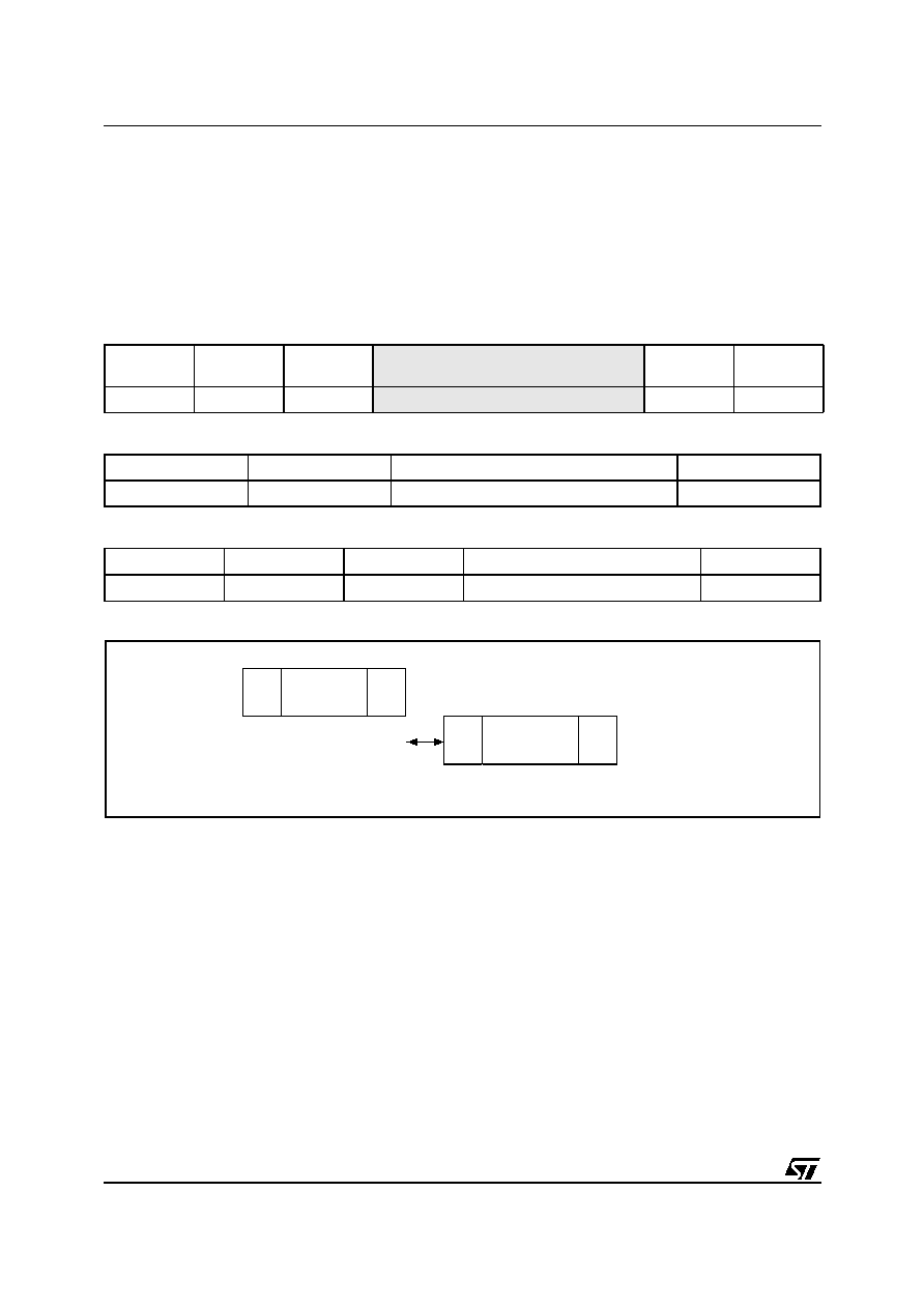
UNIQUE IDENTIFIER (UID)
The LRI512s are uniquely identified by a 64-bit
Unique Identifier (UID). This UID complies with
ISO/IEC 15963 and ISO/IEC 7816-6. The UID is a
read only code, and comprises:
≠ The 8 MSB is E0h
≠ The IC Manufacturer code of ST 02h, on 8 bits
(ISO/IEC 7816-6/AM1)
≠ A Unique Serial Number on 48 bits.
The UID is used for addressing each LRI512
uniquely and individually, during the anti-collision
loop and for one-to-one exchange between a VCD
and a LRI512.
Table 5. UID Format
APPLICATION FAMILY IDENTIFIER (AFI)
The AFI (Application Family Identifier) describes
the type of application targeted by the VCD, and is
used to extract from all the LRI512s present only
the LRI512s meeting the required application cri-
teria.
It is programmed by the LRI512 issuer in the AFI
register. Once programmed and Locked, it cannot
be modified.
The most significant nibble of AFI is used to code
one specific or all application families.
The least significant nibble of AFI is used to code
one specific or all application sub-families. Sub-
family codes, other than 0, are proprietary.
(See ISO 15693-3 documentation)
Figure 28. LRI512 Decision Tree for AFI
CRC
The CRC used in the LRI512 is calculated as per
the definition in ISO/IEC 13239.
The initial register content is all ones: FFFFh.
The 2-byte CRC is appended to each Request and
each Response, within each frame, before the
EOF. The CRC is calculated on all the bytes after
the SOF up to the CRC field.
Upon reception of a Request from the VCD, the
LRI512 verifies that the CRC value is valid. If it is
invalid, it discards the frame, and does not answer
the VCD.
Upon reception of a Response from the LRI512, it
is recommended that the VCD verify that the CRC
value is valid. If it is invalid, actions to be per-
formed are left to the responsibility of the VCD de-
signer.
The CRC is transmitted Least Significant Byte first.
Each byte is transmitted Least Significant Bit first.
Table 6. CRC Transmission Rules
MSB
LSB
63
56
55
48 47
0
E0h
02h
Unique Serial Number
AI06679
Inventory Request
Received
No
No Answer
Yes
No
AFI value
= 0 ?
Yes
No
AFI Flag
Set ?
Yes
Answer given by the LRI512
to the Inventory Request
AFI value
= Internal
value ?
LSByte
MSByte
LSBit MSBit
LSBit MSBit
CRC 16 (8bits)
CRC 16 (8 bits)
LRI512
16/54
LRI512 PROTOCOL DESCRIPTION
The Transmission protocol defines the mecha-
nism to exchange instructions and data between
the VCD and the LRI512, in both directions.
It is based on the concept of "VCD talks first".
This means that any LRI512 does not start trans-
mitting unless it has received and properly decod-
ed an instruction sent by the VCD.
The protocol is based on an exchange of
≠ a Request from the VCD to the LRI512
≠ a Response from the LRI512 to the VCD
Each Request and each Response is contained in
a Frame. The frame delimiters (SOF, EOF) are de-
scribed in the previous paragraphs.
Each Request consists of
≠ Request SOF (see Figure 9 and Figure 10)
≠ Flags
≠ A Command Code
≠ Parameters, depending on the Command
≠ Application data
≠ 2-byte CRC
≠ Request EOF (see Figure 11)
Each Response consists of
≠ Answer SOF (see Figure 20 to Figure 23)
≠ Flags
≠ Parameters, depending on the Command
≠ Application data
≠ 2-byte CRC
≠ Answer EOF (see Figure 24 to Figure 27)
The protocol is bit-oriented. The number of bits
transmitted in a frame is a multiple of eight (8) ≠
that is, an integer number of bytes.
A single-byte field is transmitted Least Significant
Bit (LSBit) first.
A multiple-byte field is transmitted Least Signifi-
cant Byte (LSByte) first, each byte is transmitted
Least Significant Bit (LSBit) first.
The setting of the flags indicates the presence of
the optional fields. When the flag is set (to one),
the field is present. When the flag is reset (to zero),
the field is absent.
Table 7. VCD Request Frame Format
Table 8. LRI512 Response Frame Format
Figure 29. LRI512 Protocol Timing
Request
SOF
Request Flags
Command Code
Parameters
Data
2 Bytes
CRC
Request
EOF
Response
SOF
Response
Flags
Parameters
Data
2 Bytes
CRC
Response
EOF
AI06830
VCD
Request Frame
(Table 7)
Request Frame
(Table 7)
LRI512
Response Frame
(Table 8)
Response Frame
(Table 8)
Timing
t1
t2
t1
t2
17/54
LRI512
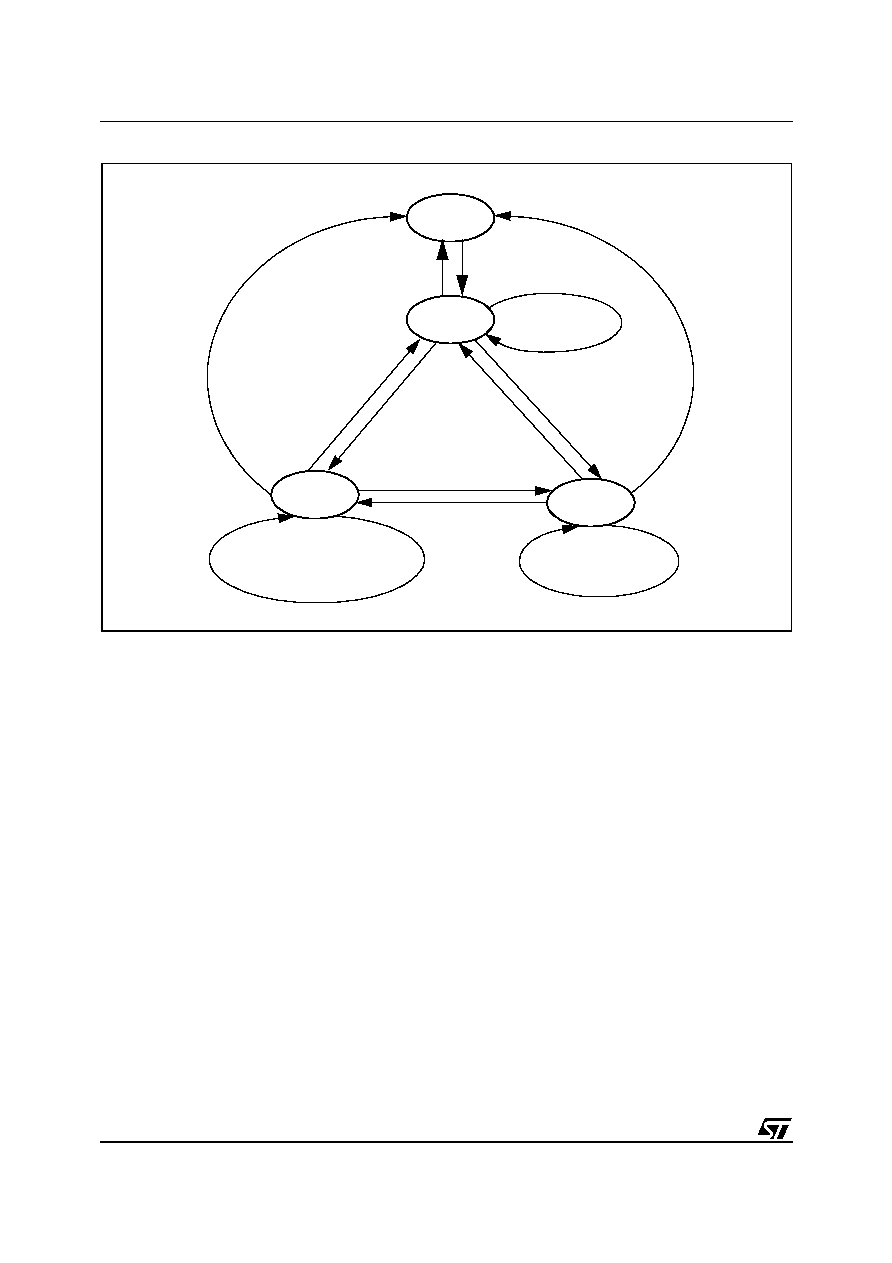
LRI512 STATES
A LRI512 can be in one of four states:
≠ Power-off
≠ Ready
≠ Quiet
≠ Selected
Transitions between these states are specified in
Figure 30 and Table 9.
Power-off State
The LRI512 is in the Power-off state when it does
not receive enough energy from the VCD.
Ready State
The LRI512 is in the Ready state when it receives
enough energy from the VCD. It shall answer any
Request where the Select_Flag is not set.
Quiet State
When in the Quiet State, the LRI512 answers any
Request other than an Inventory Request with the
Address_Flag set.
Selected State
In the Selected State, the LRI512 answers to any
Request in all modes:
≠ Request in Select mode with the Select flag set
≠ Request in Addressed mode if the UID match.
≠ Request in Non-Addressed mode as it is gener-
al Request.
Table 9. LRI512 Response, Depending on the States of the Request Flags
Flags
Address_Flag
Select_Flag
1
Addressed
0
Non Addressed
1
Selected
0
Non Selected
LRI512 in Ready or Selected state (Devices
in Quiet state do not answer)
X
X
LRI512 in Selected state
X
X
LRI512 in Ready, Quiet or Selected state (the
device which match the UID)
X
X
Error (03h)
X
X
LRI512
18/54
Figure 30. LRI512 State Transition Diagram
Note: The intention of the state transition method is that only one LRI512 should be in the selected state at a time.
AI06681
Power Off
In field
Out of field
Ready
Quiet
Selected
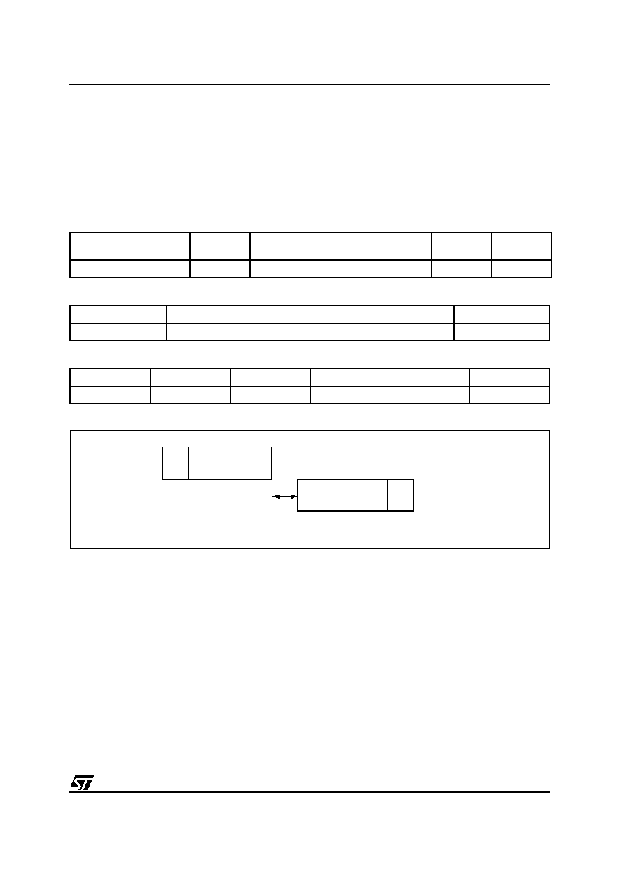
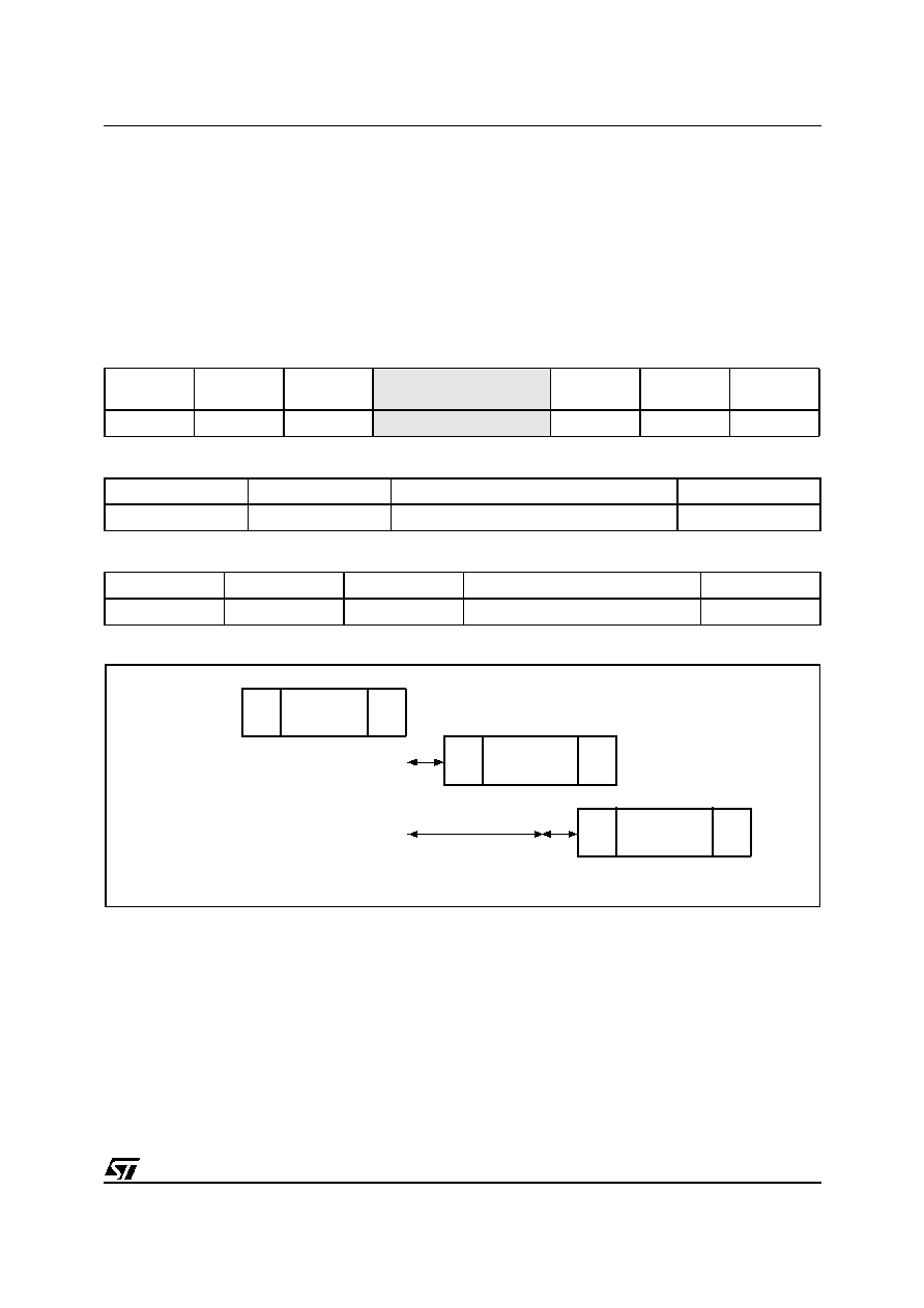
Any other Command
where Select_Flag
is not set
Out of field
Out of field
Stay quiet(UID)
Select (UID)
Any other command
Any other command where the
Address_Flag is set AND
where Inventory_Flag is not set
Stay quiet(UID)
Select (UID)
Reset to ready where
Select_Flag is set or
Select(different UID)
Reset to ready

19/54
LRI512
MODES
The set of LRI512s that can answer a given Re-
quest are those whose current "Mode" is the ap-
propriate one for that request.
Addressed Mode
When the Address_flag is set to 1 (addressed
mode), the Request shall contain the Unique ID
(UID) of the addressed LRI512.
Any LRI512 receiving a Request with the
Address_flag set to 1 shall compare the received
Unique ID to its own UID.
If it matches, it shall execute it (if possible) and re-
turn a Response to the VCD as specified by the
command description.
If it does not match, it shall remain silent.
Non-Addressed mode (General Request)
When the Address_flag is set to 0 (non-addressed
mode), the Request shall not contain a Unique ID.
Any LRI512 receiving a Request with the
Address_flag set to 0 executes it and returns a Re-
sponse to the VCD as specified by the command
description.
Select Mode
When the Select_flag is set to 1 (select mode), the
Request shall not contain a LRI512 Unique ID.
The LRI512 in the Selected State receiving a Re-
quest with the Select_flag set to 1 executes it and
returns a Response to the VCD as specified by the
command description.
Only LRI512s in the Selected State answer to a
Request having the Select Flag set to 1.
The system design ensures in theory that only one
LRI512 can be in the Select state.
LRI512
20/54
REQUEST FORMAT
The Request consists of
≠ SOF
≠ Flags
≠ A Command Code
≠ Parameters and Data
≠ CRC
≠ EOF
Table 10. General Request Format
Request Flags
In a Request, the flags field specifies the actions to
be performed by the LRI512, and whether corre-
sponding fields are present or not.
It consists of eight bits.
The bit 3 (Inventory_flag) of the request flag de-
fines the content of the 4 MSBs (bits 5 to 8).
When bit 3 is reset (0), bits 5 to 8 define the
LRI512 selection criteria.
When bit 3 is set (1), bits 5 to 8 define the LRI512
Inventory parameters.
Table 11. Request Flags 1 to 4 Definition
Note: 1. Sub-carrier_flag refers to the LRI512-to-VCD communi-
cation.
2. Data_rate_flag refers to the LRI512-to-VCD communica-
tion
Table 12. Request Flags 5 to 8 when Bit 3 = 0
Note: if the Select_flag is set to 1, the Address_flag shall be set to
0 and the UID field shall not be present in the Request.
Table 13. Request Flags 5 to 8 when Bit 3 = 1
S
O
F
Request
Flags
Command
Code
Parameters
Data
CRC
E
O
F
Bit 1
Sub-carrier
flag
0
A single sub-carrier frequency
shall be used by the LRI512
1
Two sub-carriers shall be used
by the LRI512
Bit 2
Data_rate
flag
0
Low data rate is used
1
High data rate is used
Bit 3
Inventory
flag
0
Flags 5 to 8 meaning are
according to Table 12
1
Flags 5 to 8 meaning are
according to Table 13
Bit 4
Protocol
Extension
flag
0
No Protocol format extension
Bit 5
Select flag
0
Request shall be executed by
any LRI512 according to the
setting of Address_flag
1
Request shall be executed only
by LRI512 in Selected State
Bit 6
Address
flag
0
Request is not addressed. UID
field is not present. It shall be
executed by all LRI512.
1
Request is addressed. UID field
is present. It shall be executed
only by the LRI512 whose UID
matches the UID specified in
the Request.
Bit 7 Option flag
0
Bit 8
RFU
0
Bit 5
AFI flag
0
AFI field is not present
1
AFI field is present
Bit 6 Nb_slots flag
0
16 slots
1
1 slot
Bit 7
Option flag
0
Bit 8
RFU
0
21/54
LRI512
RESPONSE FORMAT
The Response consists of
≠ SOF
≠ Flags
≠ Parameters and Data
≠ CRC
≠ EOF
Table 14. General Response Format
Response Flags
In a Response, the flags field indicates how ac-
tions have been performed by the LRI512 and
whether corresponding fields are present or not. It
consists of eight bits.
Table 15. Response Flags 1 to 8 definition
Response Error Code
If the Error Flag is set by the LRI512 in the Re-
sponse, the Error Code field is present and pro-
vides information about the error that occurred.
The following error codes are specified. Other
codes are reserved for future use.
Table 16. Response Error Code Definition
SOF
Response
Flags
Parameters
Data
CRC EOF
Bit 1
Error flag
0
No error
1
Error detected. Error code is
in the "Error" field.
Bit 2
RFU
0
Bit 3
RFU
0
Bit 4
Extension
flag
0
No extension
Bit 5
RFU
0
Bit 6
RFU
0
Bit 7
RFU
0
Bit 8
RFU
0
Error
Code
Meaning
03h
The option is not supported
10h
The specified block is not available
11h
The specified block is already locked and thus
cannot be locked again
12h
The specified block is locked and its content
cannot be changed.
LRI512
22/54
ANTI-COLLISION
The purpose of the anti-collision sequence is to in-
ventory the LRI512s present in the VCD field by
their unique ID (UID).
The VCD is the master of the communication with
one or multiple LRI512s. It initiates LRI512 com-
munication by issuing the Inventory Request.
The LRI512 sends its Response in the slot deter-
mined, or might not respond.
Request parameters
When issuing the Inventory Command, the VCD
shall:
≠ set the Nb_slots_flag to the desired setting,
≠ add after the Command Field the Mask Length
and the Mask Value,
≠ The Mask Length is the number of significant
bits of the Mask Value.
≠ The Mask Value is contained in an integer num-
ber of bytes. The Mask Length indicates the
number of significant bits. LSB shall be transmit-
ted first.
≠ If the Mask Length is not a multiple of 8 bits, the
Mask Value MSB shall be padded with the re-
quired number of null bits (set to 0) so that the
Mask Value is contained in an integer number of
bytes.
≠ The next field starts on the next byte boundary.
Table 17. Inventory Request Format
In the example of the Table 18 and Figure 31, the
Mask Length is 11 bits. The Mask Value MSB is
padded with five bits set to 0. The 11 bits Mask
plus the current slot number is compared to the
UID.
Table 18. Example of the Padding of a 11 bits
Mask Value
MSB
LSB
SOF
Request
Flags
Command
Optional AFI
Mask
Length
Mask Value
CRC
EOF
8 bits
8 bits
8 bits
8 bits
0 to 8 bytes
16 bits
(b
15
) MSB
LSB (b
0
)
0000 0
100 1100 1111
Pad
11 bits Mask Value
23/54
LRI512
Figure 31. Principle of Comparison between the Mask, Slot Number and UID
The AFI field shall be present if the AFI_flag is set.
The pulse shall be generated according to the def-
inition of the EOF in ISO/IEC 15693-2.
The first slot starts immediately after the reception
of the Request EOF.
To switch to the next slot, the VCD sends an EOF.
The following rules and restrictions apply:
≠ if no LRI512 answer is detected, the VCD may
switch to the next slot by sending an EOF
≠ if one or more LRI512 answers are detected, the
VCD shall wait until the complete frame has
been received before sending an EOF for
switching to the next slot.
AI06682
Mask value received in the Inventory command
0000 0100 1100 1111 b 16 bits
The Mask value less the padding 0s is loaded
into the Tag comparator
100 1100 1111 b 11 bits
The Slot counter is calculated
xxxx
Nb_slots_flags = 0 (16 slots), Slot Counter is 4 bits
The Slot counter is concatened to the Mask value
xxxx 100 1100 1111 b
Nb_slots_flags = 0
15 bits
The concatenated result is compared with
the least significant bits of the Tag UID.
xxxx xxxx ..... xxxx xxxx x xxx xxxx xxxx xxxx
64 bits
LSB
MSB
b
LSB
MSB
LSB
MSB
LSB
MSB
b0
b63
Compare
Bits ignored
UID
4 bits

LRI512
24/54
REQUEST PROCESSING BY THE LRI512
Upon reception of a valid Request, the LRI512
performs the following algorithm, where:
≠ NbS is the total number of slots (1 or 16)
≠ SN is the current slot number (0 to 15)
≠ LSB (value, n) function returns the n least signif-
icant bits of the value
≠ MSB (value, n) function returns the n most sig-
nificant bits of the value
≠ "&" is the concatenation operator
≠ Slot_Frame is either a SOF or an EOF
SN = 0
if (Nb_slots_flag)
then
NbS = 1
SN_length = 0
endif
else
NbS = 16
SN_length = 4
endif
label1:
if LSB(UID, SN_length + Mask_length) =
LSB(SN,SN_length)&LSB(Mask,Mask_length)
then
answer to inventory request
endif
wait (Slot_Frame)
if Slot_Frame = SOF
then
Stop Anticollision
decode/process request
exit
endif
if Slot_Frame = EOF
if SN < NbS-1
thenSN = SN + 1
goto label1
exit
endif
endif
EXPLANATION OF THE POSSIBLE CASES
Figure 32 summarizes the main possible cases
that can occur during an anti-collision sequence
when the slot number is 16.
The different steps are:
≠ The VCD sends an Inventory Request, in a
frame, terminated by an EOF. The number of
slots is 16.
≠ LRI512 #1 transmits its Response in Slot 0. It is
the only one to do so, therefore no collision oc-
curs and its UID is received and registered by
the VCD;
≠ The VCD sends an EOF, meaning to switch to
the next slot.
≠ In slot 1, two LRI512s, #2 and #3, transmit their
Responses. This generates a collision. The
VCD records it, and remembers that a collision
was detected in Slot 1.
≠ The VCD sends an EOF, meaning to switch to
the next slot.
≠ In Slot 2, no LRI512 transmits a Response.
Therefore the VCD does not detect a LRI512
SOF and decides to switch to the next slot by
sending an EOF.
≠ In slot 3, there is another collision caused by
Responses from LRI512 #4 and #5
≠ The VCD then decides to send a Request (for
instance a Read Block) to LRI512 #1, whose
UID was already correctly received.
≠ All LRI512s detect a SOF and exit the anti-colli-
sion sequence. They process this Request and
since the Request is addressed to LRI512 #1,
only LRI512 #1 transmits its Response.
≠ All LRI512s are ready to receive another Re-
quest. If it is an Inventory command, the slot
numbering sequence restarts from 0.
Note: the decision to interrupt the anti-collision se-
quence is up to the VCD. It could have continued
to send EOFs until Slot 15 and then send the Re-
quest to LRI512 #1.
25/54
LRI512
Figure 32. Description of a Possible Anti-collision Sequence
AI06831
S
lot 0
Slo
t 1
S
lot 2
Slo
t 3
VCD
SO
F
Inven
tory
Requ
est
EO
F
E
OF
EOF
E
O
F
SOF
Req
uest to
LR
I512 1
EO
F
Respo
nse
2
Resp
onse
4
LRI51
2s
Resp
onse
fr
om
LRI5
12 1
Re
spon
se
1
Respo
nse
3
Resp
onse
5
Ti
m
i
n
g
t1
t2
t1
t2
t3
t1
t2
t1
Comm
ent
No
c
o
llisio
n
Collis
ion
No
Re
spon
se
Coll
ision
Ti
m
e
LRI512
26/54
TIMING DEFINITION
t
1
: LRI512 Response Delay
t
1
is as defined in Table 19.
Upon detection of the rising edge of the EOF re-
ceived from the VCD, the LRI512 wait for a time
equal to
t
1
(typ) = 4352/f
C
(see Table 59)
before starting to transmit its response to a VCD
request or switch to the next slot when in an inven-
tory process.
The EOF is defined in page 7.
t
2
: VCD New Request Delay
t
2
is the time after which the VCD may send an
EOF to switch to the next slot when one or more
LRI512 responses have been received during an
inventory command. It starts from the reception of
the EOF received from the LRI512s.
The EOF sent by the VCD may be either 10% or
100% modulated independent of the modulation
index used for transmitting the VCD request to the
LRI512.
t
2
is also the time after which the VCD may send a
new request to the LRI512 as described in Figure
29., LRI512 Protocol Timing, on page 16.
t
2
(min) = 4192/f
C
(see Table 59)
t3: VCD New Request Delay when No LRI512
Response
t
3
is the time after which the VCD may send an
EOF to switch to the next slot when no LRI512 re-
sponse has been received.
The EOF sent by the VCD may be either 10% or
100% modulated independent of the modulation
index used for transmitting the VCD request to the
LRI512.
From the time the VCD has generated the rising
edge of an EOF:
≠ If this EOF is 100% modulated, the VCD shall
wait a time at least equal to t
3minimum
before
sending a subsequent EOF.
≠ If this EOF is 10% modulated, the VCD shall
wait a time at least equal to the sum of t
3minimum
+ the nominal response time of a LRI512, which
depend on the LRI512 data rate and subcarrier
modulation mode before sending a subsequent
EOF.
Table 19. Timing Values (see Table 59)
Note: 1.
t
SOF
is the duration for the LRI512 to transmit an SOF to
the VCD.
t
SOF
is dependant on the current data rate:
High data rate or Low data rate.
2.
t
1
(max)
does not apply for write alike requests. Timing
conditions for write alike requests are defined in the com-
mand description.
3. The tolerance of specific timings is ± 32/f
C
.
Min.
Nominal
Max.
t
1
t
1
(min)
t
1
(typ)
t
1
(max)
t
2
t
2
(min)
--
--
t
3
t
1
(max) + t
SOF
(notes
1,2
)
--
--
27/54
LRI512
COMMAND CODES
The LRI512 supports the following command
codes:
Table 20. Command Codes
Command Code
Function
0x01
Inventory
0x02
Stay Quiet
0x20
Read Single Block
0x21
Write Single Block
0x22
Lock Block
0x25
Select
0x26
Reset to Ready
0x27
Write AFI
0x28
Lock AFI
0xA0
Activate EAS
0xA1
De-activate EAS
0xA2
POOL EAS
LRI512
28/54
INVENTORY
Command Code = 0x01
When receiving the Inventory request, the LRI512
performs the anti-collision sequence. The
Inventory_flag shall be set to 1. The Meaning of
Flags 5 to 8 is according to Table 13., Request
Flags 5 to 8 when Bit 3 = 1, on page 20. The Re-
quest (Table 21) contains:
≠ Flags,
≠ Inventory Command code
≠ AFI if the AFI flag is set
≠ Mask Length
≠ Mask Value
≠ CRC
The Response (Table 22) contains:
≠ Flags
≠ DSFID (always 00h)
≠ Unique ID
Note on Inventory Operation. In the current
LRI512 device, it is not possible to use the full
range of Mask Length capability to covert the com-
plete INVENTORY sequence. Values above the
ones mentioned are not allowed:
≠ 16 slots mode (Request flag b
6
=0): Mask
Length must be in the range 0 to 27.
≠ 1 slot mode (Request flag b
6
=1): Mask
Length must be in the range 0 to 20.
STMicroelectronics programs the UID in such a
way that it guarantees that the anti-collision se-
quence is able to detect all LRI512 in the reader
field.
Table 21. Inventory Request Format
Table 22. Inventory Response Format
Request
SOF
Request
Flags
Inventory
Optional AFI
Mask Length
Mask Value
CRC16
Request
EOF
8 bits
0x01
8 bits
8 bits
0 - 64 bits
16 bits
Response
SOF
Response
Flags
DSFID
UID
CRC16
Response
EOF
8 bits
0x00
64 bits
16 bits
29/54
LRI512
STAY QUIET
Command Code = 0x02
When receiving the Stay Quiet command, the
LRI512 enters the Quiet State, and does
not
send
back a Response. There is
no
response to the
Stay Quiet Command.
When in the Quiet State:
≠ the LRI512 does not process any Request if
Inventory_flag is set,
≠ the LRI512 processes any addressed Re-
quest
The LRI512 exits the Quiet State when:
≠ reset (power off)
≠ receiving a Select request. It then goes to the
Selected state
≠ receiving a Reset to Ready request. It then
goes to the Ready state.
The Stay Quiet Command (Table 23) shall always
be executed in Addressed Mode (Select_Flag is
set to 0 and Address_Flag is set to 1).
Table 23. Stay Quiet Request Format
Figure 33. STAY QUIET Frame Exchange between VCD and LRI512
Request
SOF
Request
Flags
Stay Quiet
UID
CRC16
Request
EOF
8 bits
0x02
64 bits
16 bits
AI06842
VCD
SOF
Stay Quiet
Request
EOF
LRI512
30/54
READ SINGLE BLOCK
Command Code = 0x20
When receiving the Read Single Block Command,
the LRI512 read the requested block and send
back its 32 bits value in the Response.The
Option_Flag is supported.
Request parameter (Table 24):
≠ Option_Flag
≠ UID (Optional)
≠ Block Number
Response parameter (Table 25):
≠ Block Locking Status if Option_Flag is set
≠ 4 bytes of Block Data
Response parameter (Table 27):
≠ Error Code as Error_Flag is set
Table 24. Read Single Block Request Format
Table 25. Read Single Block Response Format when Error_Flag is NOT Set
Table 26.
Table 27. Read Single Block Response Format when Error_Flag is Set
Figure 34. READ Single Block Frame Exchange between VCD and LRI512
Request
SOF
Request
Flags
Read Single
Block
UID
Block
Number
CRC16
Request
EOF
8 bits
0x20
64 bits
8 bits
16 bits
Response
SOF
Response
Flags
Block
Locking
Status
Data
CRC16
Response
EOF
8 bits
8 bits
32 bits
16 bits
b
7
(bit b
0
for ISO)
b
6
b
5
b
4
b
3
b
2
b
1
b
0
0: Current Block not locked
1: Current Block locked
Reserved for future used. All at 0
Response SOF
Response_Flags
Error Code
CRC16
Response EOF
8 bits
8 bits
16 bits
AI06832
VCD
LRI512
t1
SOF
Read Single
Block Request
EOF
SOF
Read Single
Block Response
EOF
31/54
LRI512
WRITE SINGLE BLOCK
Command Code = 0x21
When receiving the Write Single Block Command,
the LRI512 writes the requested block with the
data contained in the Request, and reports the
success of the operation in the Response. The
Option_Flag is not supported.
During the write cycle, t
W
, no modulation (neither
100% nor 10%) shall occur, otherwise the LRI512
may program the data incorrectly in the memory.
The t
W
delay is a multiple of t
1nominal
.
Request parameter (Table 28):
≠ UID (Optional)
≠ Block Number
≠ Data
Response parameter (Table 29):
≠ No parameter. The response is sent back af-
ter the write cycle
Response parameter (Table 30):
≠ Error Code as Error_Flag is set
Table 28. Write Single Block Request Format
Table 29. Write Single Block Response Format when Error Flag is NOT Set
Table 30. Write Single Block Response Format when Error Flag is Set
Figure 35. WRITE Single Block Frame Exchange between VCD and LRI512
Request
SOF
Request
Flags
Write Single
Block
UID
Block
Number
Data
CRC16
Request
EOF
8 bits
0x21
64 bits
8 bits
32 bits
16bits
Response SOF
Response_Flags
CRC16
Response EOF
8 bits
16 bits
Response SOF
Response_Flags
Error Code
CRC16
Response EOF
8 bits
8 bits
16 bits
AI06833
VCD
LRI512
LRI512
t1
EOF
SOF
Write Single
Block Request
EOF
SOF
Write Single
Block Response
Write sequence when error
SOF
Write Single
Block Response
EOF
t1
tw
LRI512
32/54
LOCK BLOCK
Command Code = 0x22
When receiving the Lock Block Command, the
LRI512 lock permanently the requested block. The
Option_Flag is not supported.
During the write cycle t
W
, no modulation (never
100% nor 10%) shall occur. If so, the LRI512 may
not lock correctly the memory block. The t
W
delay
is a multiple of t
1nominal
.
Request parameter (Table 31):
≠ (Optional) UID
≠ Block Number
Response parameter (Table 32):
≠ No parameter.
Response parameter (Table 33):
≠ Error Code as Error_Flag is set
Table 31. Lock Single Block Request Format
Table 32. Lock Block Response Format when Error Flag is NOT Set
Table 33. Lock Block Response Format when Error Flag is Set
Figure 36. LOCK Block Frame Exchange between VCD and LRI512
Request
SOF
Request
Flags
Lock Block
UID
Block
Number
CRC16
Request
EOF
8 bits
0x22
64 bits
8 bits
16 bits
Response SOF
Response_Flags
CRC16
Response EOF
8 bits
16 bits
Response SOF
Response_Flags
Error Code
CRC16
Response EOF
8 bits
8 bits
16 bits
AI06834
VCD
LRI512
LRI512
t1
EOF
SOF
EOF
SOF
Lock sequence when error
SOF
EOF
t1
tw
Lock Block
Request
Lock Block
Response
Lock Block
Response
33/54
LRI512
SELECT
Command Code = 0x25
When receiving the Select Command:
≠ if the UID is equal to its own UID, the LRI512 en-
ter or stay in the Selected state and send a Re-
sponse.
≠ if it is different, the selected LRI512 return to the
Ready state and do not send a Response.
Request parameter (Table 34):
≠ UID
Response parameter (Table 35):
≠ No parameter.
Response parameter (Table 36):
≠ Error Code as Error_Flag is set
Table 34. Select Request Format
Table 35. Select Block Response Format when Error Flag is NOT Set
Table 36. Select Response Format when Error Flag is Set
Figure 37. SELECT Frame Exchange between VCD and LRI512
Request
SOF
Request
Flags
Select
UID
CRC16
Request
EOF
8 bits
0x25
64 bits
16 bits
Response SOF
Response_Flags
CRC16
Response EOF
8 bits
16 bits
Response SOF
Response_Flags
Error Code
CRC16
Response EOF
8 bits
8 bits
16 bits
AI06835
VCD
LRI512
t1
EOF
SOF
EOF
SOF
Select Request
Select Response
LRI512
34/54
RESET TO READY
Command Code = 0x26
When receiving a Reset to Ready Command, the
LRI512 return to the Ready state.
Request parameter (Table 37):
≠ UID (Optional)
Response parameter (Table 38):
≠ No parameter.
Response parameter (Table 39):
≠ Error Code as Error_Flag is set
Table 37. Reset to Ready Request Format
Table 38. Reset to Ready Response Format when Error Flag is NOT Set
Table 39. Reset to ready Response Format when Error Flag is Set
Figure 38. RESET to READY Frame Exchange between VCD and LRI512
Request
SOF
Request
Flags
Reset to
Ready
UID
CRC16
Request
EOF
8 bits
0x26
64 bits
16 bits
Response SOF
Response_Flags
CRC16
Response EOF
8 bits
16 bits
Response SOF
Response_Flags
Error Code
CRC16
Response EOF
8 bits
8 bits
16 bits
AI06836
VCD
LRI512
t1
SOF
Reset to Ready
Request
EOF
SOF
Reset to Ready
Response
EOF
35/54
LRI512
WRITE AFI
Command Code = 0x27
When receiving the Write AFI Request, the LRI512
write the AFI byte value into its memory. The
Option_Flag is not supported.
During the write cycle t
W
, no modulation (never
100% nor 10%) shall occur. If so, the LRI512 may
not Write correctly the AFI value into the memory.
The t
W
delay is a multiple of t
1nominal
.
Request parameter (Table 40):
≠ UID (Optional)
≠ AFI
Response parameter (Table 41):
≠ No parameter.
Response parameter (Table 42):
≠ Error Code as Error_Flag is set
Table 40. Write AFI Request Format
Table 41. Write AFI Response Format when Error Flag is NOT Set
Table 42. Write AFI Response Format when Error Flag is Set
Figure 39. WRITE AFI Frame Exchange between VCD and LRI512
Request
SOF
Request
Flags
Write AFI
UID
AFI
CRC16
Request
EOF
8 bits
0x27
64 bits
8 bits
16 bits
Response SOF
Response_Flags
CRC16
Response EOF
8 bits
16 bits
Response SOF
Response_Flags
Error Code
CRC16
Response EOF
8 bits
8 bits
16 bits
AI06837
VCD
LRI512
LRI512
t1
EOF
SOF
EOF
SOF
Write sequence when error
SOF
EOF
t1
tw
Write AFI
Request
Write AFI
Response
Write AFI
Response
LRI512
36/54
LOCK AFI
Command Code = 0x28
When receiving the Lock AFI Request, the LRI512
lock the AFI value permanently. The Option_Flag
is not supported.
During the write cycle t
W
, no modulation (never
100% nor 10%) shall occur. If so, the LRI512 may
not Lock correctly the AFI value into the memory.
The t
W
delay is a multiple of t
1nominal
.
Request parameter (Table 43):
≠ UID (Optional)
Response parameter (Table 44):
≠ No parameter.
Response parameter (Table 45):
≠ Error Code as Error_Flag is set
Table 43. Lock AFI Request Format
Table 44. Lock AFI Response Format when Error Flag is NOT Set
Table 45. Lock AFI Response Format when Error Flag is Set
Figure 40. LOCK AFI Frame Exchange between VCD and LRI512
Request
SOF
Request
Flags
Lock AFI
UID
CRC16
Request
EOF
8 bits
0x28
64 bits
16 bits
Response SOF
Response_Flags
CRC16
Response EOF
8 bits
16 bits
Response SOF
Response_Flags
Error Code
CRC16
Response EOF
8 bits
8 bits
16 bits
AI06838
VCD
LRI512
LRI512
t1
EOF
SOF
EOF
SOF
Lock sequence when error
SOF
EOF
t1
tw
Lock AFI
Request
Lock AFI
Response
Lock AFI
Response
37/54
LRI512
ACTIVATE EAS
Command Code = 0xA0
When receiving the Activate EAS Request, the
LRI512 set the non-volatile EAS bit. The
Option_Flag is not supported.
During the write cycle t
W
, no modulation (never
100% nor 10%) shall occur. If so, the LRI512 may
not set correctly the EAS bit. The t
W
delay is a mul-
tiple of t
1nominal
.
Request parameter (Table 46):
≠ UID (Optional)
Response parameter (Table 47):
≠ No parameter.
Response parameter (Table 48):
≠ Error Code as Error_Flag is set
Table 46. Activate EAS Request Format
Table 47. Activate EAS Response Format when Error Flag is NOT Set
Table 48. Activate EAS Response Format when Error Flag is Set
Figure 41. ACTIVATE EAS Frame Exchange between VCD and LRI512
Request
SOF
Request
Flags
Activate EAS
IC Mfg code
UID
CRC16
Request
EOF
8 bits
0xA0
0x02
64 bits
16 bits
Response SOF
Response_Flags
CRC16
Response EOF
8 bits
16 bits
Response SOF
Response_Flags
Error Code
CRC16
Response EOF
8 bits
8 bits
16 bits
AI06839
VCD
LRI512
LRI512
t1
EOF
SOF
EOF
SOF
Write sequence when error
SOF
EOF
t1
tw
Activate EAS
Request
Activate EAS
Response
Activate EAS
Response
LRI512
38/54
DESACTIVATE EAS
Command Code = 0xA1
When receiving the De-activate EAS Request, the
LRI512 reset the non-volatile EAS bit. The
Option_Flag is not supported.
During the write cycle t
W
, no modulation (never
100% nor 10%) shall occur. If so, the LRI512 may
not reset correctly the EAS bit. The t
W
delay is a
multiple of t
1nominal
.
Request parameter (Table 49):
≠ UID (Optional)
Response parameter (Table 50):
≠ No parameter.
Response parameter (Table 51):
≠ Error Code as Error_Flag is set
Table 49. De-activate EAS Request Format
Table 50. De-activate EAS Response Format when Error Flag is NOT Set
Table 51. De-activate EAS Response Format when Error Flag is Set
Figure 42. DE-ACTIVATE EAS Frame Exchange between VCD and LRI512
Request
SOF
Request
Flags
De-activate
EAS
IC Mfg code
UID
CRC16
Request
EOF
8 bits
0xA1
0x02
64 bits
16 bits
Response SOF
Response_Flags
CRC16
Response EOF
8 bits
16 bits
Response SOF
Response_Flags
Error Code
CRC16
Response EOF
8 bits
8 bits
16 bits
AI06840
VCD
LRI512
LRI512
t1
EOF
SOF
EOF
SOF
Write sequence when error
SOF
EOF
t1
tw
De-activate
EAS Request
De-activate
EAS Response
De-activate
EAS Response
39/54
LRI512
POOL EAS
Command Code = 0xA2
When receiving the POOL EAS Request, all
LRI512 with the non-volatile EAS bit set generate
the EAS signal.
Request parameter (Table 52 or Table 53):
≠ No parameter
Table 52. POOL EAS Request Format for One Sub-carrier Modulation Answer
Table 53. POOL EAS Request Format for Two Sub-carrier Modulation Answer
POOL EAS Response Format when the request
frame is correctly received
The LRI512 generates a continuous stream of 256
bits at `0' using the One or Two sub-carrier modu-
lation at Low data rate ended by 2 CRC bytes.
Figure 43. POOL EAS Frame Exchange between VCD and LRI512
Request SOF
Request_Flags
POOL EAS
IC Mfg code
CRC16
Request EOF
0x00
0xA2
0x02
16 bits
Request SOF
Request_Flags
POOL EAS
IC Mfg code
CRC16
Request EOF
0x01
0xA2
0x02
16 bits
AI06841
VCD
LRI512
t1
SOF
POOL EAS
Request
EOF
256 `O' using Single sub-carrier
modulation at Low data rate

LRI512
40/54
APPENDIX A
The following pseudo-code describes how the
anti-collision could be implemented on the VCD,
using recursive functions.
Algorithm for Pulsed Slots
function push (mask, address)
; pushes on private stack
function pop (mask, address)
; pops from private stack
function pulse_next_pause
; generates a power pulse
function store(LRI512_UID)
; stores LRI512_UID
function poll_loop (sub_address_size as integer)
pop (mask, address)
mask = address & mask
; generates new mask
; send the Request
mode = anti-collision
send_Request (Request_cmd, mode, mask length, mask value)
for sub_address = 0 to (2^sub_address_size - 1)
pulse_next_pause
if no_collision_is_detected
; LRI512 is inventoried
then
store (LRI512_UID)
else
; remember a collision was detected
push(mask,address)
endif
next sub_address
if stack_not_empty
; if some collisions have been detected and
then
; not yet processed, the function calls itself
poll_loop (sub_address_size)
; recursively to process the last stored
collision
endif
end poll_loop
main_cycle:
mask = null
address = null
push (mask, address)
poll_loop(sub_address_size)
end_main_cycle

41/54
LRI512
APPENDIX B
The CRC Error Detection Method
The Cyclic Redundancy Check (CRC) is calculat-
ed on all data contained in a message, from the
start of the Flags through to the end of Data. This
CRC is used from the VCD to the LRI512, and
from the LRI512 to the VCD.
Table 54. CRC Definition
To add extra protection against shift errors, a fur-
ther transformation on the calculated CRC is
made. The One's Complement of the calculated
CRC is the value attached to the message for
transmission.
For checking of received messages the two CRC
bytes are often also included in the re-calculation,
for ease of use. In this case, given the expected
value for the generated CRC is the residue of
F0B8h
CRC Calculation Example
This example in C language illustrates one method
of calculating the CRC on a given set of bytes
comprising a message.
C-Example to calculate or check the CRC16 according to ISO/IEC 13239
#define POLYNOMIAL0x8408// x^16 + x^12 + x^5 + 1
#define PRESET_VALUE0xFFFF
#define CHECK_VALUE0xF0B8
#define NUMBER_OF_BYTES4// Example: 4 data bytes
#define CALC_CRC1
#define CHECK_CRC0
void main()
{
unsigned int current_crc_value;
unsigned char array_of_databytes[NUMBER_OF_BYTES + 2] = {1, 2, 3, 4, 0x91, 0x39};
int number_of_databytes = NUMBER_OF_BYTES;
int calculate_or_check_crc;
int i, j;
calculate_or_check_crc = CALC_CRC;
// calculate_or_check_crc = CHECK_CRC;// This could be an other example
if (calculate_or_check_crc == CALC_CRC)
{
number_of_databytes = NUMBER_OF_BYTES;
}
else // check CRC
{
number_of_databytes = NUMBER_OF_BYTES + 2;
}
current_crc_value = PRESET_VALUE;
for (i = 0; i < number_of_databytes; i++)
{
current_crc_value = current_crc_value ^ ((unsigned int)array_of_databytes[i]);
for (j = 0; j < 8; j++)
{
if (current_crc_value & 0x0001)
{
CRC Definition
CRC Type
Length
Polynomial
Direction
Preset
Residue
ISO/IEC 13239
16 bits
X
16
+ X
12
+ X
5
+ 1 = Ox8408
Backward
0xFFFF
0xF0B8

LRI512
42/54
current_crc_value = (current_crc_value >> 1) ^ POLYNOMIAL;
}
else
{
current_crc_value = (current_crc_value >> 1);
}
}
}
if (calculate_or_check_crc == CALC_CRC)
{
current_crc_value = ~current_crc_value;
printf ("Generated CRC is 0x%04X\n", current_crc_value);
// current_crc_value is now ready to be appended to the data stream
// (first LSByte, then MSByte)
}
else // check CRC
{
if (current_crc_value == CHECK_VALUE)
{
printf ("Checked CRC is ok (0x%04X)\n", current_crc_value);
}
else
{
printf ("Checked CRC is NOT ok (0x%04X)\n", current_crc_value);
}
}
}
43/54
LRI512
APPENDIX C
Application Family Identifier (AFI)
The AFI (Application Family Identifier) represents
the type of application targeted by the VCD and is
used to extract from all the LRI512 present only
the LRI512 meeting the required application crite-
ria.
It is programmed by the LRI512 issuer (the pur-
chaser of the LRI512). Once locked, it cannot be
modified.
The most significant nibble of AFI is used to code
one specific or all application families, as defined
in Table 55.
The least significant nibble of AFI is used to code
one specific or all application sub-families. Sub-
family codes other than 0 are proprietary.
Table 55. AFI Coding
Note: X = 1h to Fh, Y = 1h to Fh
AFI
Most
Significant
Nibble
AFI
Least
Significant
Nibble
Meaning
VICCs respond from
Examples / Note
0
0
All families and sub-families
No applicative preselection
`X'
0
All sub-families of family X
Wide applicative preselection
`X'
`Y'
Only the Yth sub-family of family X
0
`Y'
Proprietary sub-family Y only
1
0, `Y'
Transport
Mass transit, Bus, Airline,...
2
0, `Y'
Financial
IEP, Banking, Retail,...
3
0, `Y'
Identification
Access Control,...
4
0, `Y'
Telecomunication
Public Telephony, GSM,...
5
0, `Y'
Medical
6
0, `Y'
Multimedia
Internet services....
7
0, `Y'
Gaming
8
0, `Y'
Data Storage
Portable Files, ...
9
0, `Y'
Item Management
A
0, `Y'
Express Parcels
B
0, `Y'
Postal Services
C
0, `Y'
Airline Bags
D
0, `Y'
RFU
E
0, `Y'
RFU
F
0, `Y'
RFU
LRI512
44/54
MAXIMUM RATING
Stressing the device above the rating listed in the
Absolute Maximum Ratings table may cause per-
manent damage to the device. These are stress
ratings only and operation of the device at these or
any other conditions above those indicated in the
Operating sections of this specification is not im-
plied. Exposure to Absolute Maximum Rating con-
ditions for extended periods may affect device
reliability. Refer also to the STMicroelectronics
SURE Program and other relevant quality docu-
ments.
Table 56. Absolute Maximum Ratings
Note: 1. IPC/JEDEC J-STD-020A
2. ESD test: ISO10373-7 specification
Symbol
Parameter
Condition
Min.
Max.
Unit
T
STG
Storage Temperature
W4
ST antistatic bag,
max 23 months
15
25
∞C
SB
Mounted wafer in a wafer-
sawing box (8"),
max 25 wafers
15
25
∞C
A1T/ISOR
40-60% RH, max 2 Years
15
25
∞C
A1S/ISOR
Reels in shrink film and
packed in hexagonal
cardboard box
15
25
∞C
A2T/ISOK
40% RH, max 1 year
15
25
∞C
C40
Reels in ST cardboard box
15
25
∞C
V
MAX
Maximum Input Voltage on AC0 / AC1
≠7
7
V
V
ESD
Electrostatic Discharge
Voltage
2
A1T/ISOR
ISO 10373-7
≠7000
7000
V
A1S/ISOR
ISO 10373-7
≠7000
7000
V
A2T/ISOK
ISO 10373-7
≠7000
7000
V
C40
ISO 10373-7
≠7000
7000
V
45/54
LRI512
DC AND AC PARAMETERS
This section summarizes the operating and mea-
surement conditions, and the DC and AC charac-
teristics of the device. The parameters in the DC
and AC Characteristic tables that follow are de-
rived from tests performed under the Measure-
ment Conditions summarized in the relevant
tables. Designers should check that the operating
conditions in their circuit match the measurement
conditions when relying on the quoted parame-
ters.
Table 57. Operating Conditions
Symbol
Parameter
Min.
Max.
Unit
T
A
Ambient Operating
Temperature
A1T/ISOR
≠20
85
∞C
A1S/ISOR
≠20
85
∞C
A2T/ISOK
≠20
85
∞C
C40
≠20
85
∞C
LRI512
46/54
Figure 44. LRI512 Synchronous Timing, Transmit and Receive
Figure 44 shows an ASK modulated signal, from
the VCD to the LRI512. The test condition for the
AC/DC parameters are:
≠ Close coupling condition with tester antenna
(1mm)
≠ Gives LRI512 performance on tag antenna
Table 58. DC Characteristics
AI06680
A
B
tRFF
tRFR
tRFSBL
tMAX
tMIN CD
fCC
Symbol
Parameter
Test Condition (in addition to
those in Table 57)
Min.
Typ.
Max.
Unit
V
CC
Regulated Voltage
1.5
3.0
V
V
RET
Retromodulated
Induced Voltage
A1T/ISOR
ISO10373-7
10
mV
A1S/ISOR
ISO10373-7
10
mV
A2T/ISOK
ISO10373-7
10
mV
C40
ISO10373-7
10
mV
I
CC
Supply Current (Active in Read)
Vcc = 3.0V
150
µA
I
CC
Supply Current (Active in Write)
Vcc = 3.0V
400
µA
C
TUN
Internal Tuning Capacitor
f=13.56Mhz for W4/22
18.5
pF
C
TUN
Internal Tuning Capacitor
f=13.56Mhz for W4/30
26
pF
47/54
LRI512
Table 59. AC Characteristics
Note: 1. P
A
Min is the minimum H-field required to communicate with the LRI512
P
A
Max is the maximum H-field that the device can support before clamping the incoming signal
Symbol
Parameter
Test Condition (in addition to
those in Table 57)
Min.
Typ.
Max.
Unit
f
CC
External RF Signal Frequency
13.553
13.56
13.567
MHz
MI
CARRIER
10% Carrier Modulation Index
MI=(A-B)/(A+B)
10
30
%
t
RFR
, t
RFF
10% Rise and Fall time
0
3.0
µs
t
RFSBL
10% Minimum Pulse Width for
bit
7.1
9.44
µs
MI
CARRIER
100% Carrier Modulation Index
MI=(A-B)/(A+B)
95
100
%
t
RFR
, t
RFF
100% Rise and Fall time
0
3.5
µs
t
RFSBL
100% Minimum Pulse Width for
bit
7.1
9.44
µs
t
JIT
Bit pulse Jitter
-2
+2
µs
t
MAX
Maximum Carrier Rise Time
Zero to Maximum field strength
induced Voltage on Coil
3
V/µs
t
MINCD
Minimum Time from Carrier
Generation to First Data
From H-field min
0.1
1
ms
f
SH
Subcarrier Frequency High
F
CC
/32
423.75
kHz
f
SL
Subcarrier Frequency Low
F
CC
/28
484.28
kHz
t
1
Time for LRI512 Response
4224/F
S
313
320.9
322
µs
t
2
Time between Commands
4224/F
S
309
311.5
314
µs
r
L
Resistive Load (for Modulation)
500
1000
2000
P
A
H-field Energy on LRI512
Antenna
A1T/ISOR
0.15
5
A/m
A1S/ISOR
0.15
5
A/m
A2T/ISOK
0.15
5
A/m
C40
1
5
A/m
t
W
Programming Time
5
ms
LRI512
48/54
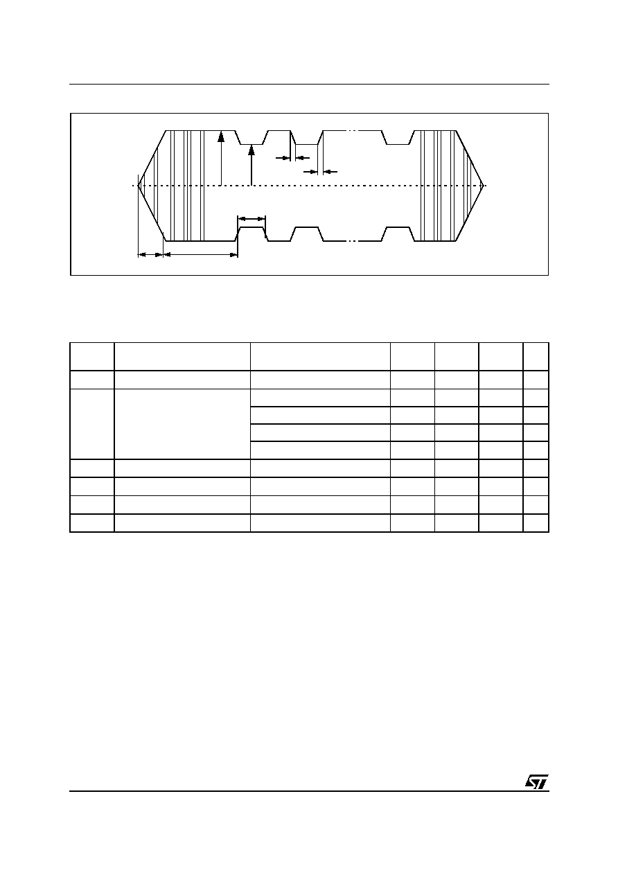
PACKAGE MECHANICAL
A1T/ISOR ≠ Copper Antenna, Package Outline
Note: Drawing is not to scale.
A1T/ISOR ≠ Copper Antenna, Package Mechanical Data
Symbol
millimeters
inches
Typ
Min
Max
Typ
Min
Max
A1
(Coil Width)
45
44.5
45.5
1.772
1.752
1.791
A2
(Coil Length)
76
75.5
76.5
2.992
2.972
3.012
C
(Web Width)
48
47.5
48.5
1.890
1.870
1.909
D
(Pitch)
96
95.5
96.5
3.780
3.760
3.800
E
(Coil distance from
Web edge)
1.5
1
2
0.059
0.039
0.079
(Overall Thickness of
copper antenna coil)
0.110
0.090
0.130
0.004
0.003
0.005
(Silicon Thickness)
0.180
0.165
0.195
0.007
0.006
0.008
Q
(Unloaded Q value)
35
35
F
NOM
(Unloaded free-air
resonance)
14.6 MHz
14.6 MHz
AI06843
A2
D
C
E
A1
49/54
LRI512
A1S/ISOR ≠ Copper Antenna, Package Outline
Note: Drawing is not to scale.
A1S/ISOR ≠ Copper Antenna, Package Mechanical Data
Symbol
millimeters
inches
Typ
Min
Max
Typ
Min
Max
A1
(Coil Width)
45
44.5
45.5
1.772
1.752
1.791
A2
(Coil Length)
76
75.5
76.5
2.992
2.972
3.012
C
(Web Width)
48
47.5
48.5
1.890
1.870
1.909
D
(Pitch)
96
95.5
96.5
3.780
3.760
3.800
E
(Coil distance from
Web edge)
1.5
1
2
0.059
0.039
0.079
(Overall Thickness of
copper antenna coil)
0.110
0.090
0.130
0.004
0.003
0.005
(Silicon Thickness)
0.180
0.165
0.195
0.007
0.006
0.008
Q
(Unloaded Q value)
35
35
F
NOM
(Unloaded free-air
resonance)
14.6 MHz
14.6 MHz
AI06843
A2
D
C
E
A1
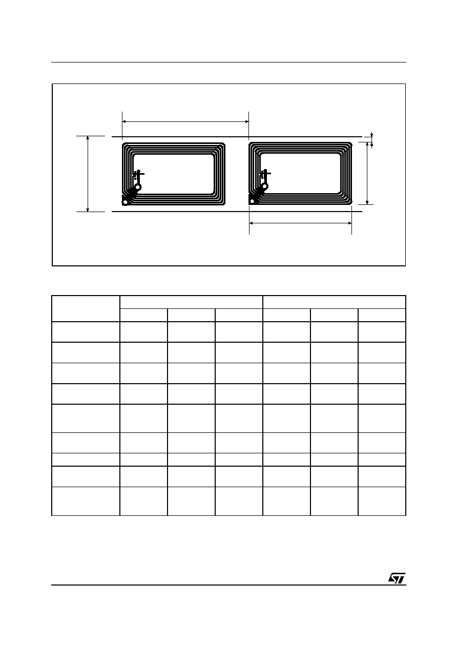
LRI512
50/54
A2T/ISOK ≠ Aluminium Antenna, Package Outline
Note: Drawing is not to scale.
A2T/ISOK ≠ Aluminium Antenna, Package Mechanical Data
Symbol
millimeters
inches
Typ
Min
Max
Typ
Min
Max
A1
(Coil Width)
45
44.5
45.5
1.772
1.752
1.791
A2
(Coil Length)
76
75.5
76.5
2.992
2.972
3.012
C
(Web Width)
48
47.5
48.5
1.890
1.870
1.909
D
(Pitch)
96
95.5
96.5
3.780
3.760
3.800
E
(Coil distance from
Web edge)
1.5
1
2
0.059
0.039
0.079
(Overall Thickness of
copper antenna coil)
0.100
0.080
0.120
0.004
0.003
0.005
(Silicon Thickness)
0.180
0.165
0.195
0.007
0.006
0.008
Q
(Unloaded Q value)
F
NOM
(Unloaded free-air
resonance)
14.6 MHz
14.6 MHz
AI06844
A2
D
C
E
A1
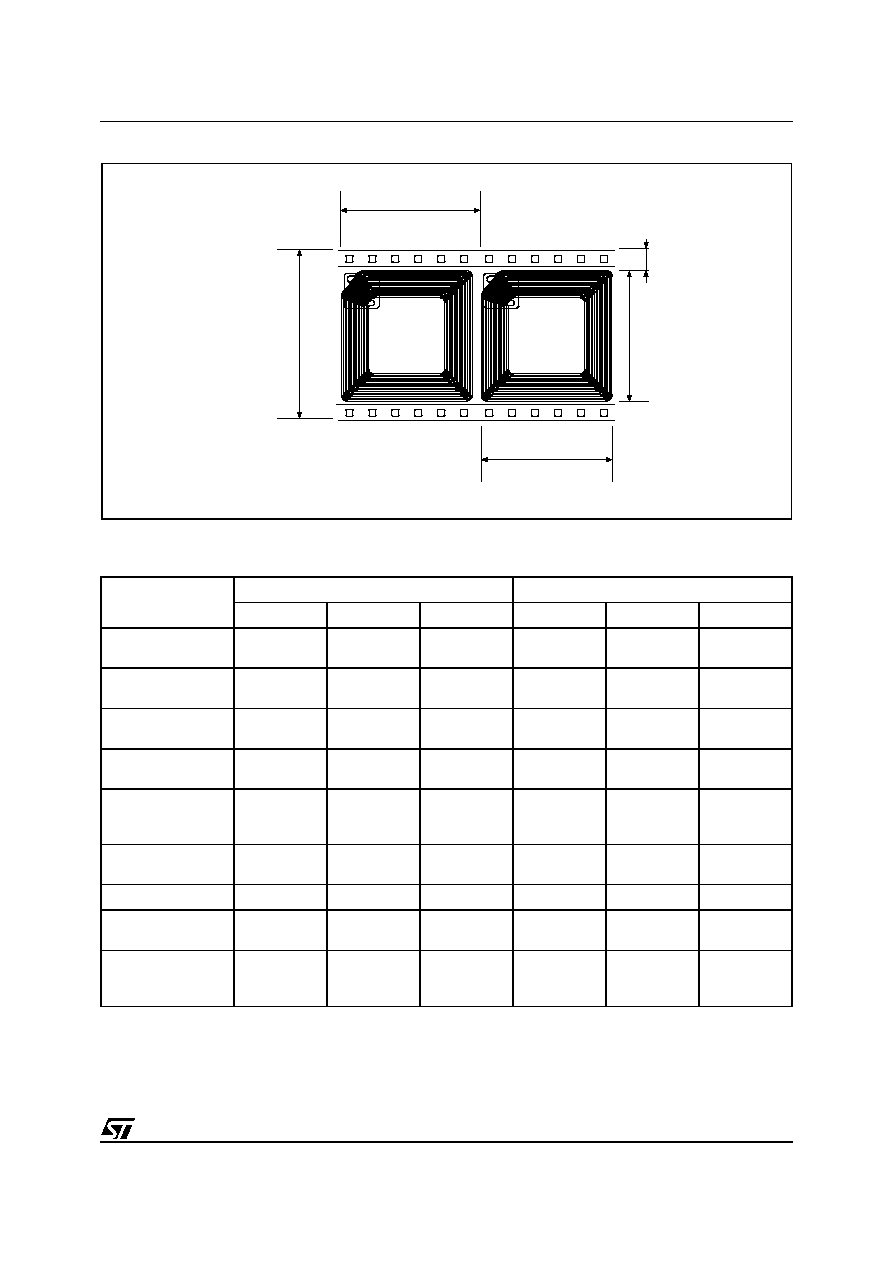
51/54
LRI512
C40 ≠ Micromodule Antenna, Package Outline
Note: Drawing is not to scale.
C40 ≠ Micromodule Antenna, Package Mechanical Data
Symbol
millimeters
inches
Typ
Min
Max
Typ
Min
Max
A1
(Coil Width)
27.5
27.4
27.6
1.083
1.079
1.087
A2
(Coil Length)
27.5
27.4
27.6
1.083
1.079
1.087
C
(Web Width)
35.0
34.9
35.1
1.378
1.374
1.382
D
(Pitch)
28.5
28.4
28.6
1.122
1.118
1.126
E
(Coil distance from
Web edge)
3.75
0.148
(Overall Thickness of
copper antenna coil)
0.190
0.187
0.193
0.007
0.007
0.008
(Silicon Thickness)
0.180
0.165
0.195
0.007
0.006
0.008
Q
(Unloaded Q value)
F
NOM
(Unloaded free-air
resonance)
14.4 MHz
14.4 MHz
AI06844
A2
D
C
E
A1

LRI512
52/54
PART NUMBERING
Table 60. Ordering Information Scheme
The notation used for the device number is as
shown in Table 60. For a list of available options
(speed, package, etc.) or for further information on
any aspect of this device, please see the current
Memory Shortform Catalogue, or contact your
nearest ST Sales Office, or email:
memories.contactless@st.com
Example:
LRI512
-
W4/22
Delivery Form
W4/22
180
µ
m ± 15
µ
m unsawn wafer, 18.5 pF tuning capacitor
W4/30
180
µ
m ± 15
µ
m unsawn wafer, 26 pF tuning capacitor
SBN18/22 180
µ
m ± 15
µ
m sawn wafer with bumps, 18.5 pF tuning capacitor, 8-inch frame
SBN16/22 180
µ
m ± 15
µ
m sawn wafer with bumps, 18.5 pF tuning capacitor, 6-inch frame
A1T/ISOR ISO Copper Antenna on tape
A1S/ISOR ISO Copper Adhesive Antenna on tape
A2T/ISOK ISO Aluminium Antenna on tape
C40
Micromodule Antenna on Super 35mm tape

53/54
LRI512
REVISION HISTORY
Table 61. Document Revision History
Date
Rev.
Description of Revision
16-Jul-2002
1.0
Document written

LRI512
54/54
Information furnished is believed to be accurate and reliable. However, STMicroelectronics assumes no responsibility for the consequences
of use of such information nor for any infringement of patents or other rights of third parties which may result from its use. No license is granted
by implication or otherwise under any patent or patent rights of STMicroelectronics. Specifications mentioned in this publication are subject
to change without notice. This publication supersedes and replaces all information previously supplied. STMicroelectronics products are not
authorized for use as critical components in life support devices or systems without express written approval of STMicroelectronics.
The ST logo is registered trademark of STMicroelectronics
All other names are the property of their respective owners
© 2002 STMicroelectronics - All Rights Reserved
STMicroelectronics group of companies
Australia - Brazil - Canada - China - Finland - France - Germany - Hong Kong -
India - Israel - Italy - Japan - Malaysia - Malta - Morocco - Singapore - Spain - Sweden - Switzerland - United Kingdom - United States.
www.st.com