 | –≠–ª–µ–∫—Ç—Ä–æ–Ω–Ω—ã–π –∫–æ–º–ø–æ–Ω–µ–Ω—Ç: LS204M | –°–∫–∞—á–∞—Ç—å:  PDF PDF  ZIP ZIP |
1/10
s
LOW POWER CONSUMPTION
s
SHORT CIRCUIT PROTECTION
s
LOW DISTORTION, LOW NOISE
s
HIGH GAIN-BANDWIDTH PRODUCT
s
HIGH CHANNEL SEPARATION
DESCRIPTION
The LS204 is a high performance dual operational
amplifier with frequency and phase compensation
built into the chip. The internal phase compensa-
tion allows stable operation as voltage follower in
spite of its high Gain-Bandwidth Product.
The circuit presents very stable electrical charac-
teristics over the entire supply voltage range, and
is particularly intended for professional and tele-
com applications (active filter, etc).
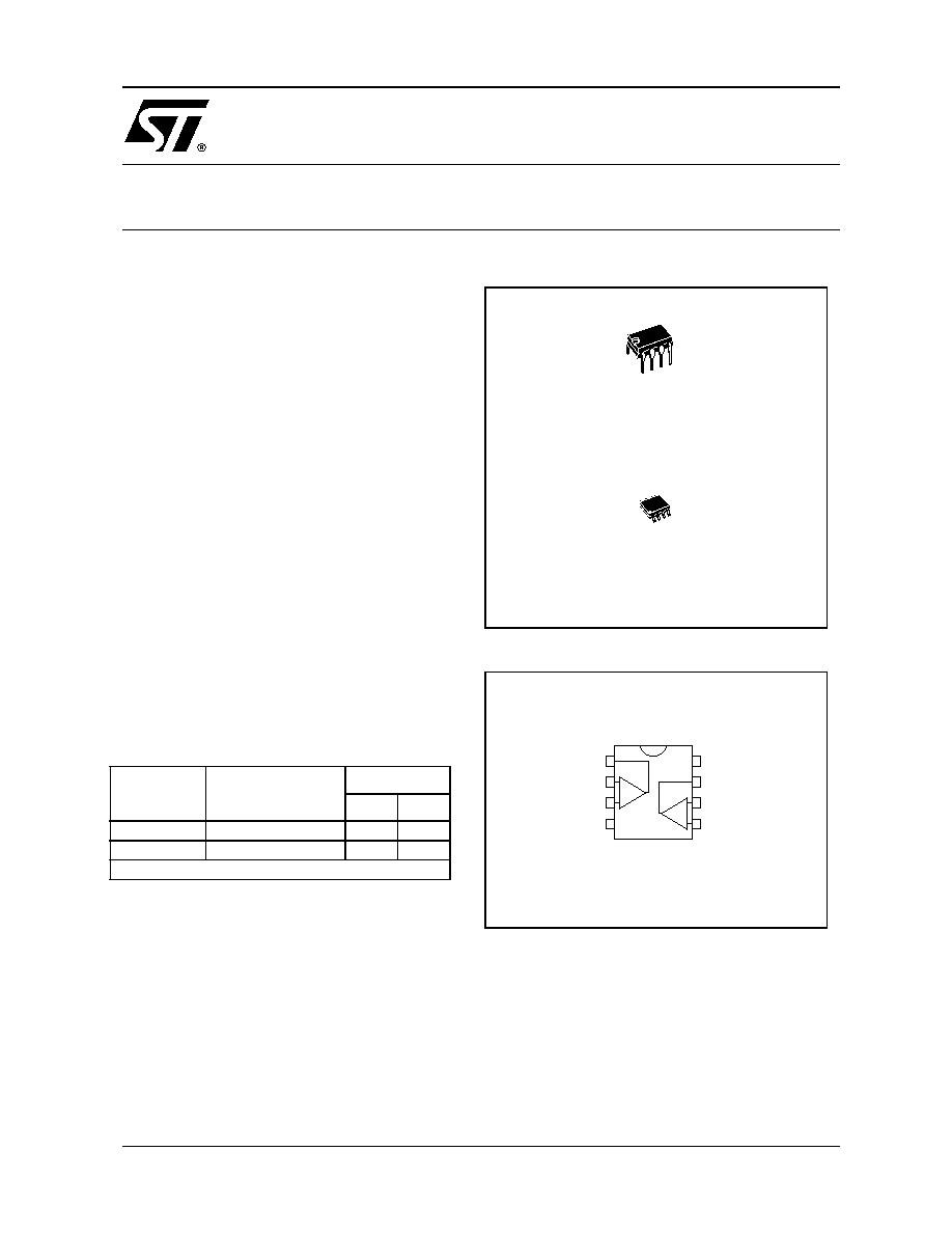
ORDER CODE
N = Dual in Line Package (DIP)
D = Small Outline Package (SO) - also available in Tape & Reel (DT)
PIN CONNECTIONS (top view)
Part Number
Temperature Range
Package
N
D
LS204C
0∞C, +70∞C
∑
∑
LS204I
-40∞C, +105∞C
∑
∑
Example : LS204CN
N
DIP8
(Plastic Package)
D
SO8
(Plastic Micropackage)
1
2
3
4
5
6
7
8
-
+
-
+
Output 1
Inverting input 1
Non-inverting input 1
V
CC
VCC
Output 2
Inverting input 2
Non-inverting input 2
-
+
HIGH PERFORMANCE
DUAL OPERATIONAL AMPLIFIER
November 2001
LS204
LS204
2/10
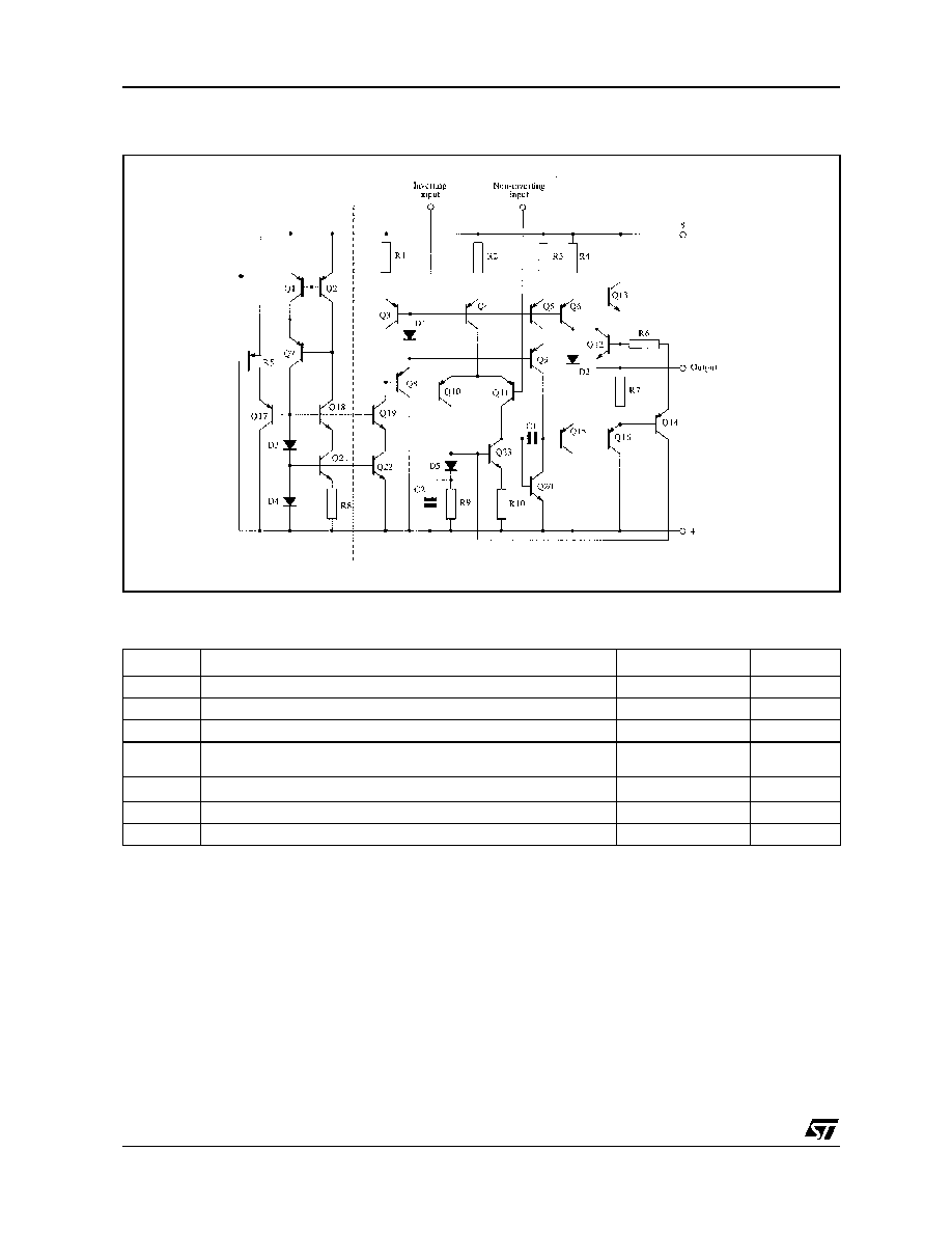
SCHEMATIC DIAGRAM (1/2 LS204)
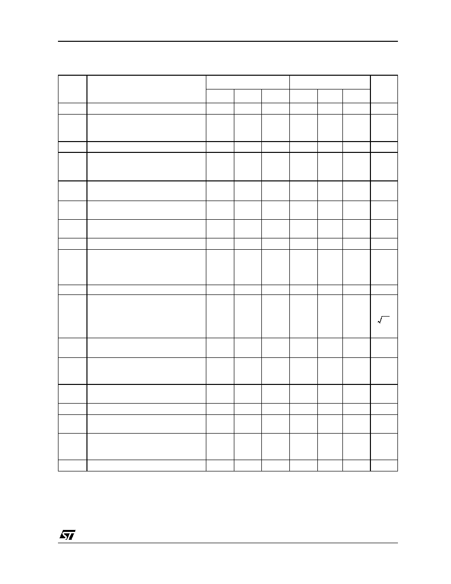
ABSOLUTE MAXIMUM RATINGS
Symbol
Parameter
Value
Unit
V
CC
Supply voltage
±18
V
V
i
Input Voltage
±V
CC
V
V
id
Differential Input Voltage
±(V
CC
-1)
V
T
oper
Operating Temperature Range
LS204C
LS204I
0 to +70
-40 to +105
∞C
P
tot
Power Dissipation at T
amb
= 70∞C
1)
500
mW
T
J
Junction Temperature
150
∞C
T
stg
Storage Temperature Range
-65 to +150
∞C
1.
Power dissipation must be considered to ensure maximum junction temperature (Tj) is not exceeded.
LS204
3/10
ELECTRICAL CHARACTERISTICS
V
CC
= ±15V, T
amb
= 25∞C (unless otherwise specified)
Symbol
Parameter
LS204I
LS204C
Unit
Min.
Typ.
Max.
Min.
Typ.
Max.
I
cc
Supply Current
0.7
1.2
0.8
1.5
mA
I
ib
Input Bias Current
T
amb
= 25∞C
T
min
<
T
op
<
T
max
50
150
300
100
300
700
nA
R
i
Input Resistance (f = 1kHz)
1
1
M
V
io
Input Offset Voltage (R
s
10k
)
T
amb
= 25∞C
T
min
<
T
op
<
T
max
0.5
2.5
3.5
0.5
3.5
5
mV
DV
io
Input Offset Voltage Drift (R
s
10k
)
T
min
<
T
op
<
T
max
5
5
µV/∞C
I
io
Input Offset Current
T
min
<
T
op
<
T
max
5
20
40
12
50
100
nA
DI
io
Input Offset Current Drift
T
min
<
T
op
<
T
max
0.08
0.1
nA/∞C
I
os
Output Short-circuit Current
23
23
mA
A
vd
Large Signal Voltage Gain
T
min
<
T
op
<
T
max
R
L
= 2k
V
CC
= ±15V
V
CC
= ±4V
90
100
95
86
100
95
dB
GBP
Gain Bandwith Product (f =100kHz)
1.8
3
1.5
2.5
MHz
e
n
Equivalent Input Noise Voltage
f = 1kHz, R
s
= 100
R
s
= 50
R
s
= 1k
R
s
= 10k
8
10
18
10
12
20
THD
Total Harmonic Distortion (f = 1kHz, A
v
=
20dB, R
L
= 2k
, V
o
= 2V
pp
)
0.03
0.03
%
±V
opp
Output Voltage Swing
R
L
= 2k
V
CC
= ±15V
V
CC
= ±4V
±13
±3
±13
±3
V
V
opp
Large Signal Voltage Swing
R
L
= 10k
, f = 10kHz
28
28
Vpp
SR
Slew Rate (R
L
= 2k
, unity gain)
0.8
1.5
1
V/
µ
s
SVR
Supply Voltage Rejection Ratio
T
min
<
T
op
<
T
max
90
86
dB
CMR
Common Mode Rejection Ratio
V
ic
= ±10V
T
min
<
T
op
<
T
max
90
86
dB
V
o1
/V
o2
Channel Separation (f= 1kHz)
100
120
120
dB
nV
Hz
------------
LS204
4/10
LS204
5/10
LS204
6/10
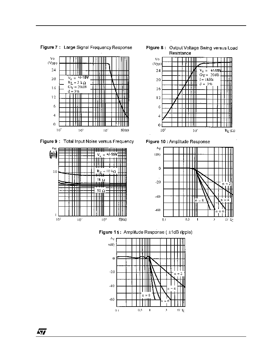
APPLICATION INFORMATION: Active low-pass filter
BUTTERWORTH
The Butterworth is a "maximally flat" amplitude re-
sponse filter (figure 10) Butterworth filters are
used for filtering signals in data acquisition sys-
tems to prevent aliasing errors in samples-data
applications and for general purpose low-pass fil-
tering.
The cut-off frequency Fc, is the frequency at which
the amplitude response is down 3dB. The attenu-
ation rate beyond the cutoff frequency is n6 dB per
octave of frequency where n is the order (number
of poles) of the filter.
Other characteristics :
u
Flattest possible amplitude response
u
Excellent gain accuracy at low frequency
end of passband
BESSEL
The Bessel is a type of "linear phase" filter. Be-
cause of their linear phase characteristics, these
filters approximate a constant time delay over a
limited frequency range. Bessel filters pass tran-
sient waveforms with a minimum of distortion.
They are also used to provide time delays for low
pass filtering of modulated waveforms and as a
"running average" type filter.
The maximum phase shift is
radians where
n is the order (number of poles) of the filter. The
cut-off frequency fc, is defined as the frequency at
which the phase shift is one half of this value.
For accurate delay, the cut-off frequency should
be twice the maximum signal frequency.
The following table can be used to obtain the -3dB
frequency of the filter.
Other characteristics :
u
Selectivity not as great as Chebyschev or
Butterworth
u
Very little overshoot response to step inputs
u
Fast rise time
CHEBYSCHEV
Chebyschev filters have greater selectivity than ei-
ther Bessel ro Butterworth at the expense of ripple
in the passband (figure 11).
Chebyschev filters are normally designed with
peak-to-peak ripple values from 0.2dB to 2dB.
Increased ripple in the passband allows increased
attenuation above the cut-off frequency.
The cut-off frequency is defined as the frequency
at which the amplitude response passes through
the specificed maximum ripple band and enters
the stop band.
Other characteristics :
u
Greater selectivity
u
Very non-linear phase response
u
High overshoot response to step inputs
The table below shows the typical overshoot and setting time response of the low pass filters to a step
input.
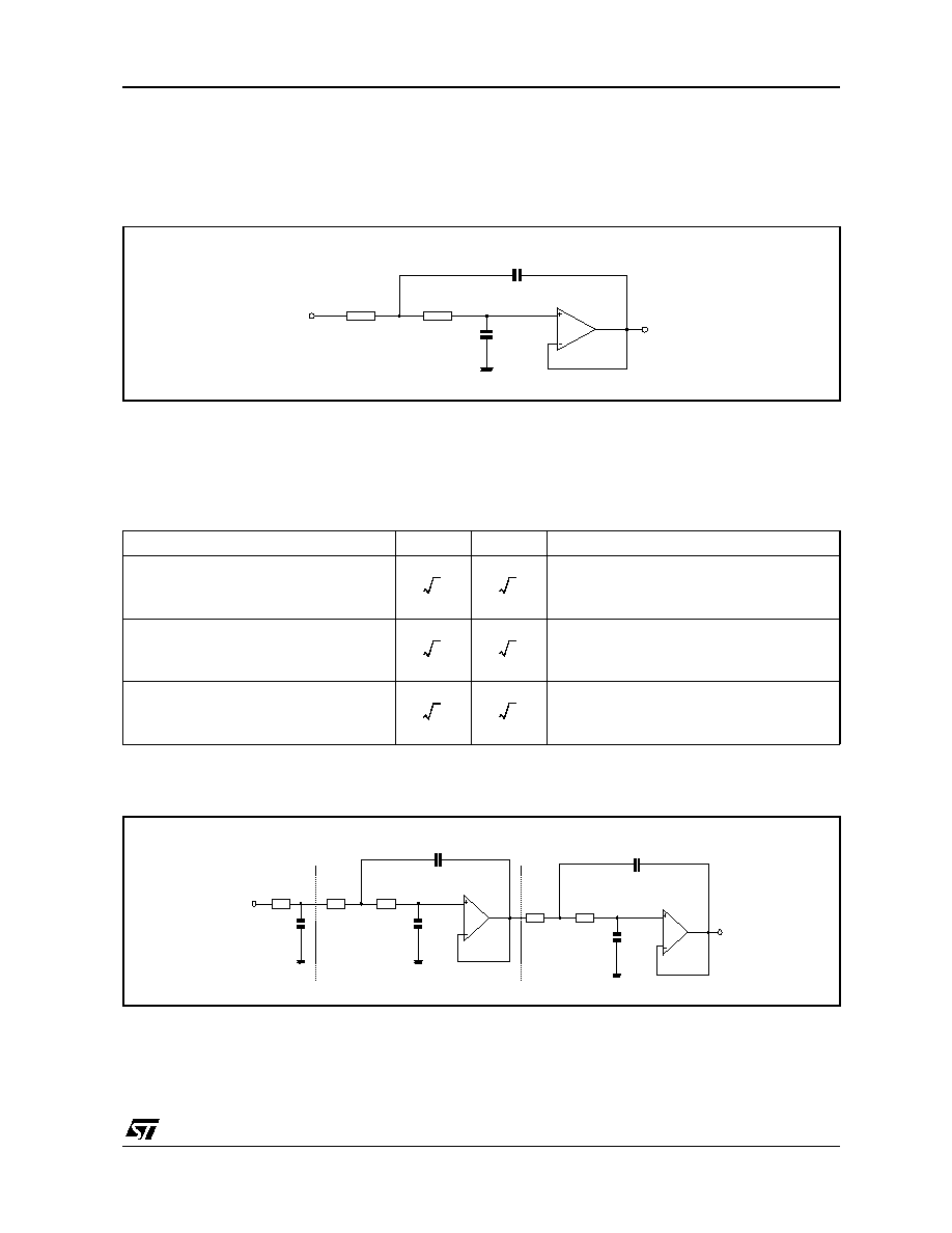
Design of 2nd order active low pass filter (Sallen and Key configuration unity gain op-amp)
n
≠
2
-----------
2 Pole
4 Pole
6 Pole
8 Pole
-3dB Frequency
0.77fc
0.67fc
0.57fc
0.50fc
Number of Poles
Peak
Overshoot
Settling Time (% of final value)
% Overshoot
±1%
±0.1%
±0.01%
Butterworth
2
4
6
8
4
11
14
14
1.1Fc sec.
1.7/fc
2.4/fc
3.1/fc
1.7Fc sec.
2.8/fc
3.9S/fc
5.1/fc
1.9Fc sec.
3.8/fc
5.0S/fc
7.1/fc
Bessel
2
4
6
8
0.4
0.8
0.6
0.1
0.8/fc
1.0/fc
1.3/fc
1.6/fc
1.4/fc
1.8/fc
2.1/fc
2.3/fc
1.7/fc
2.4/fc
2.7/fc
3.2/fc
Chebyschev (ripple ±0.25dB)
2
4
6
8
11
18
21
23
1.1/fc
3.0/fc
5.9/fc
8.4/fc
1.6/fc
5.4/fc
10.4/fc
16.4/fc
-
-
-
-
Chebyschev (ripple ±1dB)
2
4
6
8
21
28
32
34
1.6/fc
4.8/fc
8.2/fc
11.6/fc
2.7/fc
8.4/fc
16.3/fc
24.8/fc
-
-
-
LS204
7/10
Fixed R = R1 = R2, we have (see figure 12)
Figure 12 : Filter Configuration
Three parameters are needed to characterize the
frequency and phase response of a 2nd order ac-
tive filter: the gain (Gv), the damping factio (
) or
the Q factor (Q = 2
)
1
), and the cuttoff frequency
(fc).
The higher order response are obtained with a se-
ries of 2nd order sections. A simple RC section is
introduced when an odd filter is required.
The choice of '
' (or Q factor) determines the filter
response (see table 1).
Table 1
EXAMPLE
Figure 13 : 5th Order Low-pass Filter (Butterworth) with Unity Gain configuration
C
1 =
1
R
----
c
-------
C
2 =
1
R
----
1
c
-----------
C2
R2
R1
Vin
C1
Vout
Filter Response
Q
Cuttoff Frequency fc
Bessel
Frequency at which Phase Shift is -90∞C
Butterworth
Frequency at which Gv = -3dB
Chebyschev
Frequency at which the amplitude response
passes through specified max. ripple band and
enters the stop bank.
3
2
-------
1
3
-------
2
2
-------
1
2
-------
2
2
-------
1
2
-------
C2
R2
R1
C1
Ri
Ci
C4
R4
R3
C3
LS204
8/10
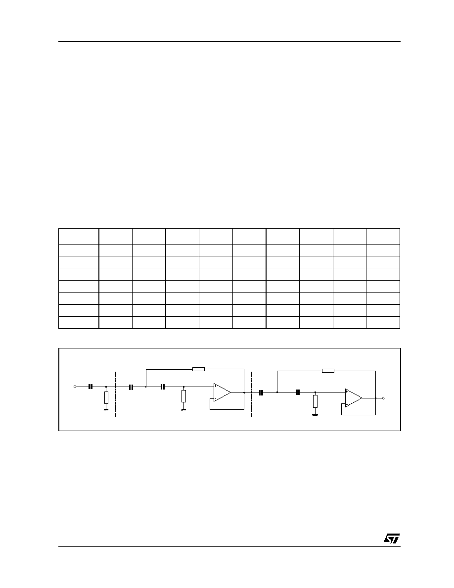
In the circuit of figure 13, for fc = 3.4kHz and R
i
=
R1 = R2 = R3 = 10k
, we obtain:
The attenuation of the filter is 30dB at 6.8kHz and
better than 60dB at 15kHz.
The same method, referring to table 2 and figure
14 is used to design high-pass filter. In this case
the damping factor is found by taking the recipro-
cal of the numbers in table 2. For fc = 5kHz and Ci
= C1 = C2 = C3 = 1nF we obtain:
Table 2 : Damping Factor for Low-pass Butterworth Filters
Figure 14 : 5th Order High-pass Filter (Butterworth) with Unity Gain configuration
Ci = 1.354
1
R
----
1
2
fc
------------ = 6.33nF
C1 = 0.421
1
R
----
1
2
fc
------------ = 1.97nF
C2 = 1.753
1
R
----
1
2
fc
------------ = 8.20nF
C3 = 0.309
1
R
----
1
2
fc
------------ = 1.45nF
C4 = 3.325
1
R
----
1
2
fc
------------ = 15.14nF
Ri =
1
0.354
---------------
1
C
----
1
2
fc
------------ = 25.5k
R1 =
1
0.421
---------------
1
C
----
1
2
fc
------------ = 75.6k
R2 =
1
1.753
---------------
1
C
----
1
2
fc
------------ = 18.2k
R3 =
1
0.309
---------------
1
C
----
1
2
fc
------------ = 103k
R4 =
1
3.325
---------------
1
C
----
1
2
fc
------------ = 9.6k
Order
Ci
C1
C2
C3
C4
C5
C6
C7
C8
2
0.707
1.41
3
1.392
0.202
3.54
4
0.92
1.08
0.38
2.61
5
1.354
0.421
1.75
0.309
3.235
6
0.966
1.035
0.707
1.414
0.259
3.86
7
1.336
0.488
1.53
0.623
1.604
0.222
4.49
8
0.98
1.02
0.83
1.20
0.556
1.80
0.195
5.125
R2
C2
C1
R1
Ri
Ci
R4
C3
R3
C4
LS204
9/10
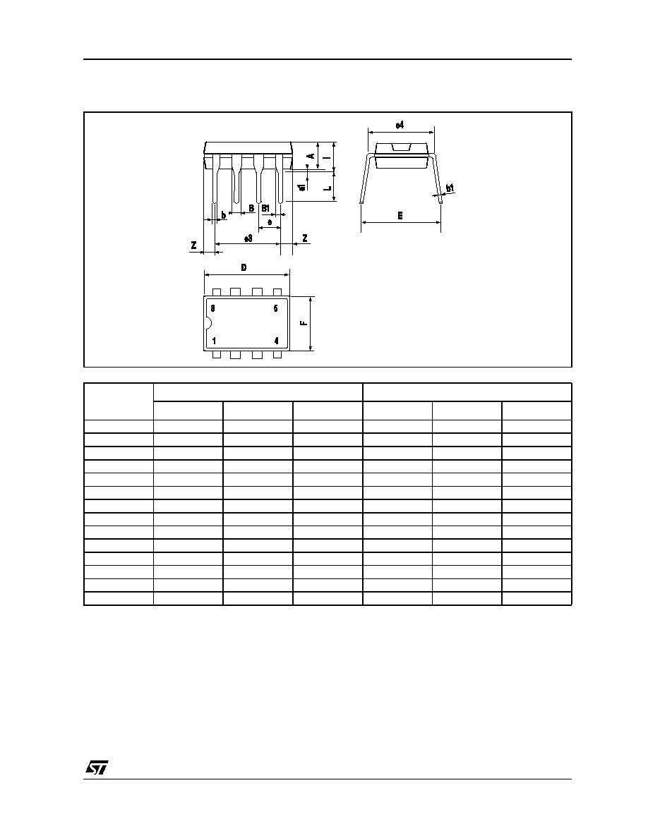
PACKAGE MECHANICAL DATA
8 PINS - PLASTIC PACKAGE
Dimensions
Millimeters
Inches
Min.
Typ.
Max.
Min.
Typ.
Max.
A
3.32
0.131
a1
0.51
0.020
B
1.15
1.65
0.045
0.065
b
0.356
0.55
0.014
0.022
b1
0.204
0.304
0.008
0.012
D
10.92
0.430
E
7.95
9.75
0.313
0.384
e
2.54
0.100
e3
7.62
0.300
e4
7.62
0.300
F
6.6
0260
i
5.08
0.200
L
3.18
3.81
0.125
0.150
Z
1.52
0.060
LS204
10/10
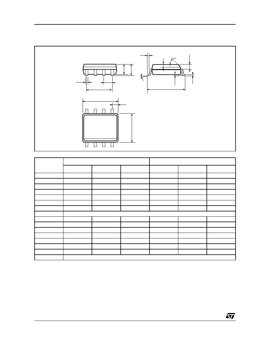
PACKAGE MECHANICAL DATA
8 PINS - PLASTIC MICROPACKAGE (SO)
Dimensions
Millimeters
Inches
Min.
Typ.
Max.
Min.
Typ.
Max.
A
1.75
0.069
a1
0.1
0.25
0.004
0.010
a2
1.65
0.065
a3
0.65
0.85
0.026
0.033
b
0.35
0.48
0.014
0.019
b1
0.19
0.25
0.007
0.010
C
0.25
0.5
0.010
0.020
c1
45∞ (typ.)
D
4.8
5.0
0.189
0.197
E
5.8
6.2
0.228
0.244
e
1.27
0.050
e3
3.81
0.150
F
3.8
4.0
0.150
0.157
L
0.4
1.27
0.016
0.050
M
0.6
0.024
S
8∞ (max.)
b
e3
A
a2
s
L
C
E
c1
a3
b1
a1
D
M
8
5
1
4
F
Information furnished is believed to be accurate and reliable. However, STMicroelectronics assumes no responsibility for the
consequences of use of such information nor for any infringement of patents or other rights of third parties which may result from
its use. No license is granted by implication or otherwise under any patent or patent rights of STMicroelectronics. Specifications
mentioned in this publication are subject to change without notice. This publication supersedes and replaces all information
previously supplied. STMicroelectronics products are not authorized for use as critical components in life support devices or
systems without express written approval of STMicroelectronics.
© The ST logo is a registered trademark of STMicroelectronics
© 2001 STMicroelectronics - Printed in Italy - All Rights Reserved
STMicroelectronics GROUP OF COMPANIES
Australia - Brazil - Canada - China - Finland - France - Germany - Hong Kong - India - Israel - Italy - Japan - Malaysia
Malta - Morocco - Singapore - Spain - Sweden - Switzerland - United Kingdom - United States
© http://www.st.com