 | –≠–ª–µ–∫—Ç—Ä–æ–Ω–Ω—ã–π –∫–æ–º–ø–æ–Ω–µ–Ω—Ç: LS256B | –°–∫–∞—á–∞—Ç—å:  PDF PDF  ZIP ZIP |
LS256
November 1996
TONE GENERATOR INTERFACE
TELEPHONE SPEECH CIRCUIT WITH MULTIFREQUENCY
.
PRESENTS THE PROPER DC PATH FOR THE
LINE CURRENT
.
HANDLES THE VOICE SIGNAL, PERFORM-
ING THE 2/4 WIRES INTERFACE
AND
CHANGING THE GAIN ON BOTH SENDING
AND RECEIVING AMPLIFIERS TO COMPEN-
SATE FOR LINE ATTENUATION BY SENSING
THELINE LENGTH THROUGH THE LINE CUR-
RENT
.
ACTS AS LINEAR INTERFACE FOR MF, SUP-
PLYING A STABILIZEDTO THE DIGITAL CHIP
AND DELIVERING TO THE LINE THE MF
TONE GENERATED BY THE DIALER
DESCRIPTION
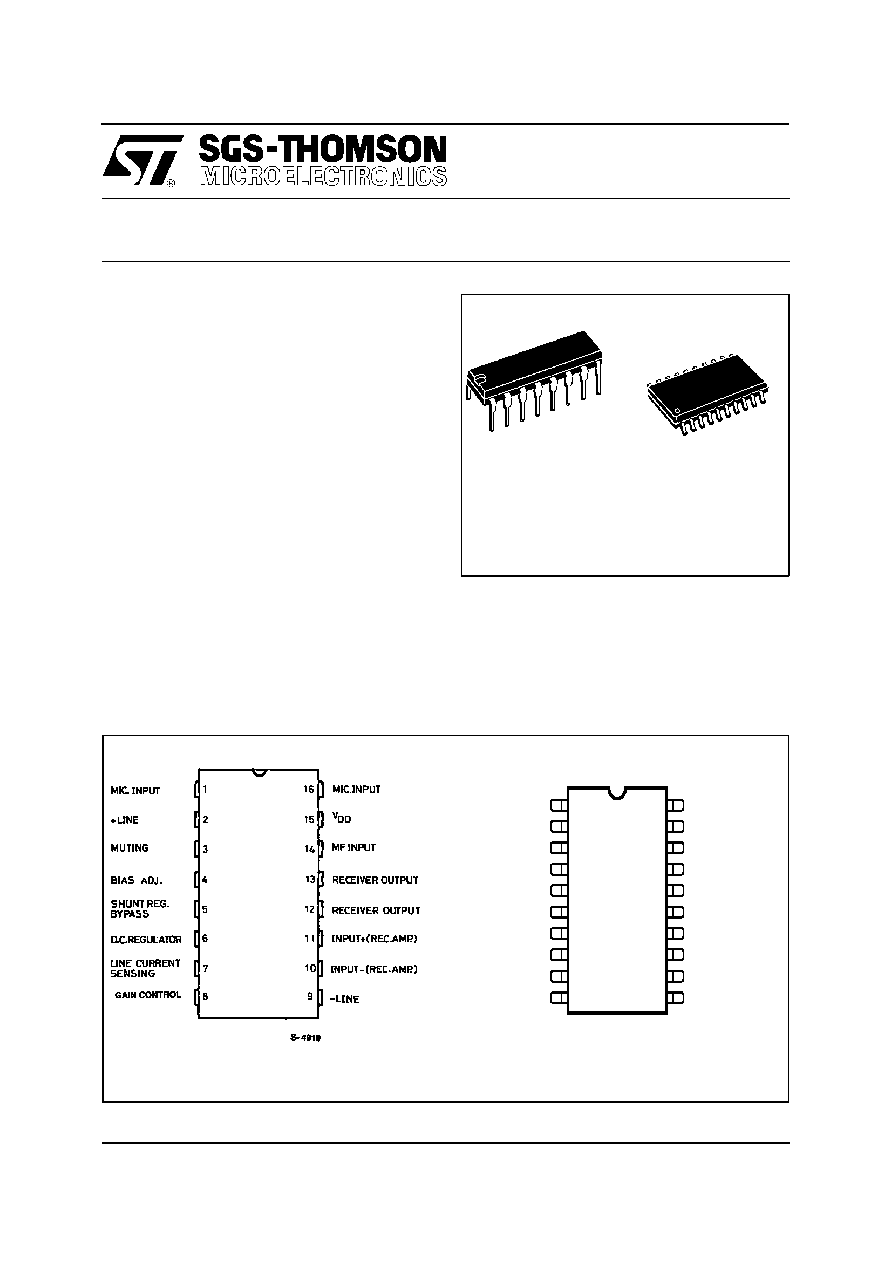
The LS256 is a monolithic integrated circuit in 16-
lead dual in-line and SO20 plastic packages to re-
placethe hybridcircuit in telephoneset. It workswith
the same type of transdurcers for both transmitter
and receiver (typically piezoceramic capsules, but
DIP16
ORDERING NUMBERS :
LS256B
LS256D
the device can work also with dynamic ones). Many
of its electrical characteristics can be controlled by
means of external components to meet different
specifications.
In addition to the speech operation, the LS256 acts
as an interface for the MF tone signal.
PIN CONNECTIONS (to p view)
DIP16
SO20
N.C.
MIC. INPUT
+LINE
MUTING
BIAS ADJ.
DC. REGULATOR
SHUNT REG. BYPASS
LINE CURRENT SENSING
GAIN CONTROL
-LINE
INPUT-(REC.AMP.)
INPUT+(REC.AMP.)
RECEIVER OUTPUT
RECEIVER OUTPUT
MF INPUT
V
DD
MIC. INPUT
N.C.
1
3
2
4
5
6
7
8
9
18
17
16
15
14
12
13
11
19
10
20
N.C.
N.C.
D96TL274
SO20
1/8
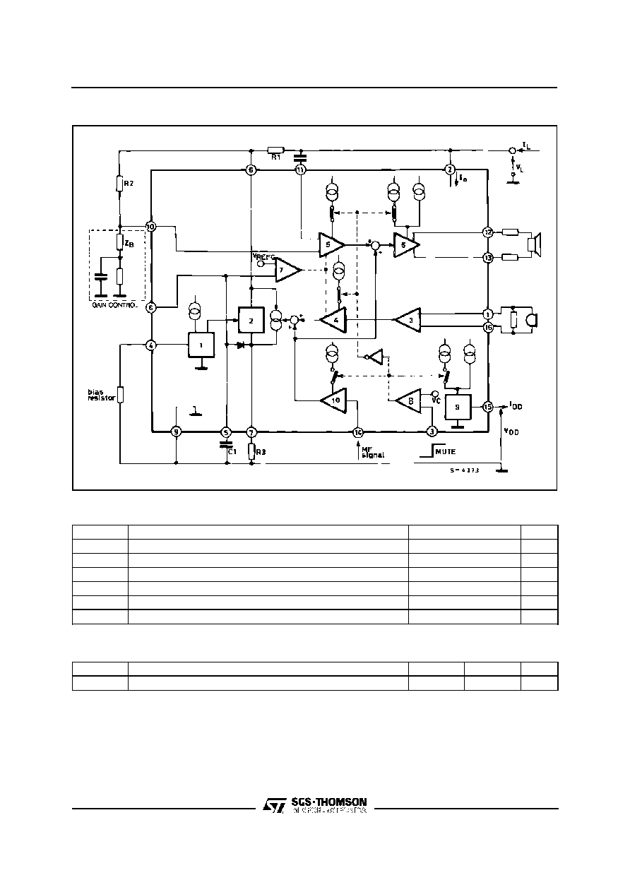
BLOCK DIAGRAM (ref. to DIP16)
ABSOLUTE MAXIMUM RATINGS
Symbol
Parameter
Value
Unit
V
L
Line Voltage (3ms pulse duration)
22
V
I
L
Forward Line Current
150
mA
I
L
Reverse Line Current
≠ 150
mA
P
tot
Total Power Dissipation at T
amb
= 70
∞
C
1
W
T
op
Operating Temperature
≠ 45 to 70
∞
C
T
stg
, T
j
Storage and Junction Temperature
≠ 65 to 150
∞
C
THERMAL DATA
Symbol
Parameter
DIP16
SO20
Unit
R
th j-amb
Thermal Resistance Junction-ambient
Max
80
150
∞
C/W
LS256
2/8
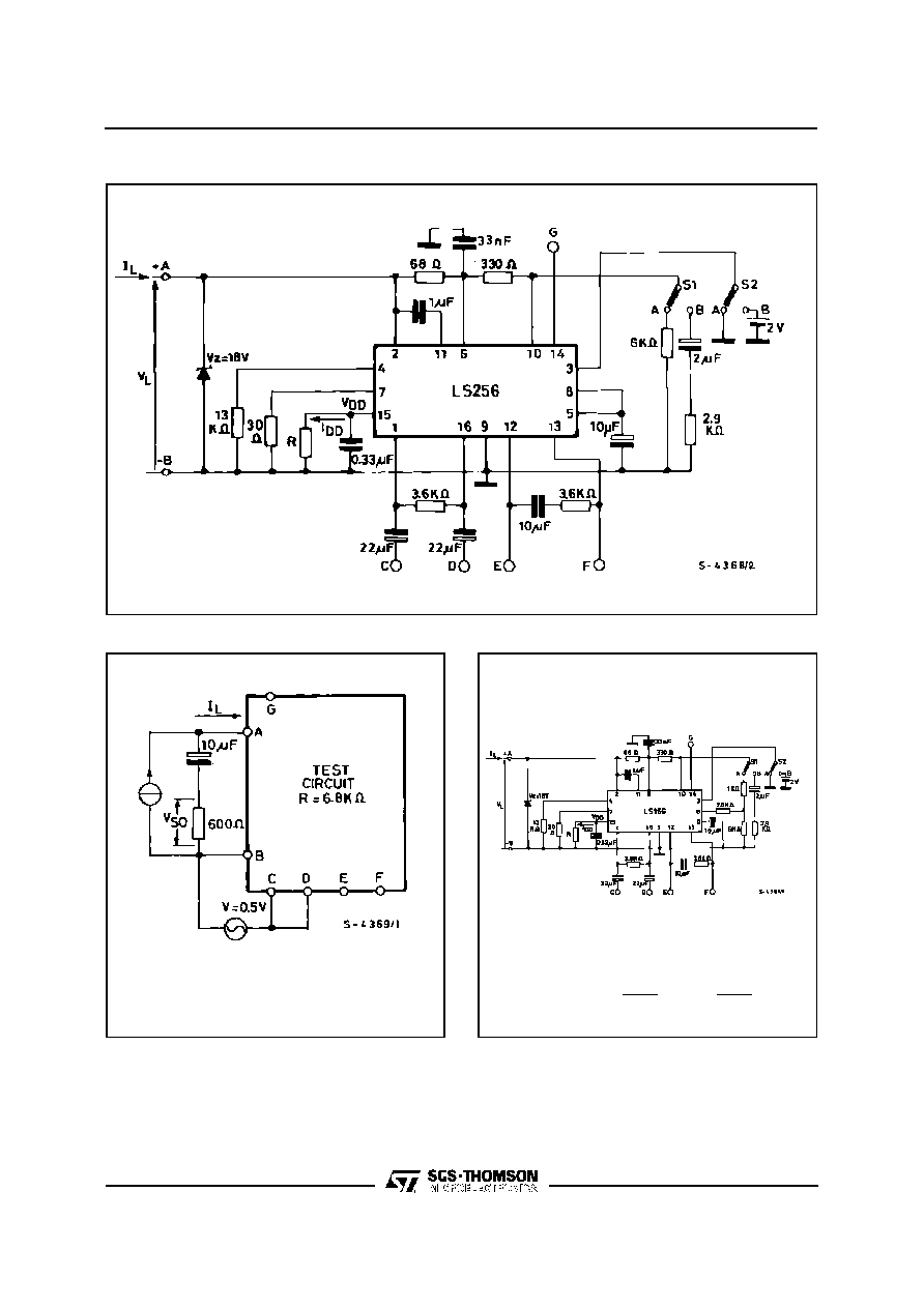
TEST CIRCUITS (ref. to DIP16)
Figure 1.
Figure 2.
V
RO
V
SO
Side tone =
; G
s
=
V
MI
V
MI
V = 0,1V ; CMRR
LS256
3/8
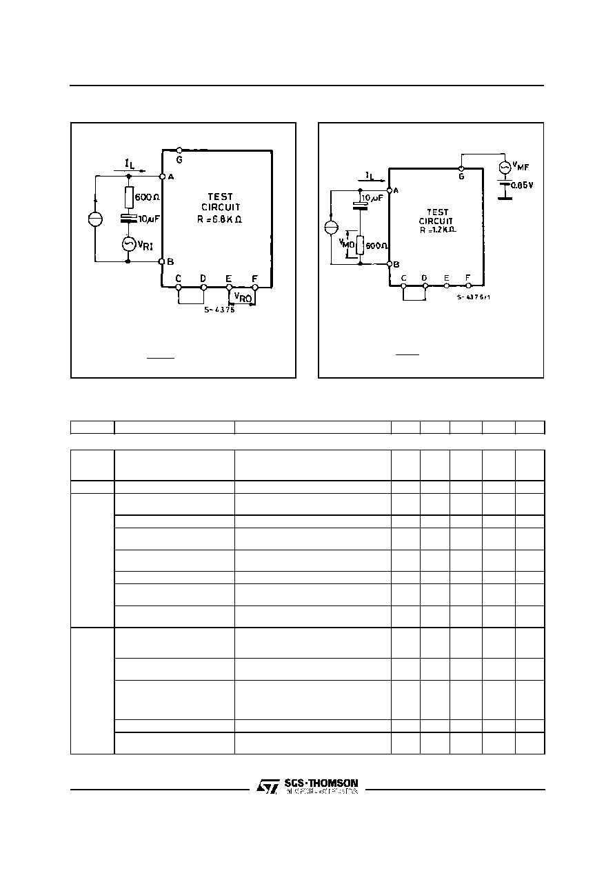
Figure 3.
Figure 4.
V
RO
G
R
=
V
RI
V
MO
G
MF
=
VMF
ELECTRICAL CHARACTERISTICS (refer to the test circuits, S1, S2 in (a),
T
amb
= ≠ 25 to + 50
o
C, f = 200 to 3400Hz, unless otherwise specified)
Symbol
Parameter
Test Conditions
Min.
Typ.
Max.
Unit
Fig.
SPEECH OPERATION
V
L
Line Voltage
T
amb
= 25
∞
C
I
L
= 12mA
I
L
= 20mA
I
L
= 80mA
3.9
4.7
5.5
12.2
V
CMRR
Common Mode Rejection
f = 1kHz, I
L
= 12 to 80mA
50
dB
1
G
S
Sending Gain
T
amb
= 25
∞
C, f = 1kHz
I
L
= 52mA
V
MI
= 2mV
I
L
= 25mA
44
48
45
49
46
50
dB
2
Sending Gain Flatness
V
MI
= 2mV, f
ref
= 1kHz
I
L
= 12 to 80mA
±
1
dB
2
Sending Distortion
f = 1kHz
V
SO
= 1V
I
L
= 16 to 80mA
V
SO
= 1.3V
2
10
%
2
Sending Noise
V
MI
= 0V; I
L
= 40mA; S1 in (b)
≠68.5
dBmp
2
Microphone Input
Impedance Pin 1-16
V
MI
= 2mV, I
L
= 12 to 80mA
40
k
Sending Loss in MF
Operation
V
MI
= 2mV
I
L
= 52mA
S
2
in (b)
I
L
= 25mA
≠ 30
≠ 30
dB
2
G
R
Receiving Gain
V
R1
= 0.3V, f = 1kHz, T
amb
= 25
∞
C
I
L
= 52mA
I
L
= 25mA
2.5
7
3.5
8
4.5
9
dB
3
Receiving Gain Flatness
V
RI
= 0.3V, f
ref
= 1kHz
I
L
= 12 to 80mA
±
1
dB
3
Receiving Distortion
f = 1kHz
I
L
= 12mA V
RO
= 1.6V
I
L
= 12mA V
RO
= 1.9V
I
L
= 50mA V
RO
= 1.8V
I
L
= 50mA V
RO
= 2.1V
2
10
2
10
%
3
Receiving Noise
V
RI
= 0V; I
L
= 12 to 80mA; S1 in (b)
100
µ
V
3
Receiver Output
Impedance Pin 12-13
V
RO
= 50mV, I
L
= 40mA
100
LS256
4/8
ELECTRICAL CHARACTERISTICS (continued)
Symbol
Parameter
Test Conditions
Min.
Typ. Max.
Unit
Fig.
SPEECH OPERATION (continued)
G
R
Sidetone
F = 1kHz, T
amb
= 25
∞
C, S
1
in (b)
I
L
= 52mA
I
L
= 25mA
36
36
dB
2
Z
ML
Line Matching Impedance
V
RI
= 0.3V, f = 1kHz
I
L
= 12 to 80mA
500
600
700
MULTIFREQUENCY SYNTHESIZER INTERFACE
V
DD
MF Supply Voltage
(standby and operation)
I
L
= 12 to 80mA
2.4
2.5
V
I
DD
MF Supply Current
Stand by
Operation
I
L
= 12 to 80mA
I
L
= 12 to 80mA ; S
2
in (b)
0.5
2
mA
mA
MF Amplifier Gain
I
L
= 12 to 80mA, f
MF
in = 1kHz
V
MF
in = 80mV
15
17
dB
4
V
I
DC Input Voltage Level (pin 14)
V
M Fin
= 80mV
3V
DD
V
R
I
Input Impedance (pin 14)
V
M Fin
= 80mV
40
k
d
Distortion
V
M Fin
= 110mV
I
L
= 12 to 80mA
2
%
4
Starting Delay Time
I
L
= 12 to 80mA
5
ms
Muting Threshold Voltage (pin 3)
Speech Operation
1
V
MF Operation
1.6
V
Muting Stand by Current (pin 3)
I
L
= 12 to 80mA
≠ 10
µ
A
Muting Operating Current (pin 3)
I
L
= 12 to 80mA, S
2
in (b)
+ 10
µ
A
LS256
5/8
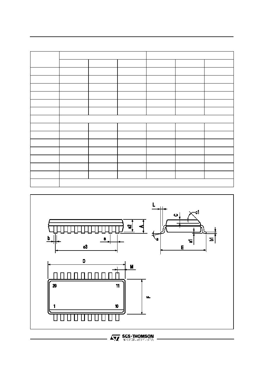
SO20 PACKAGE MECHANICAL DATA
DIM.
mm
inch
MIN.
TYP.
MAX.
MIN.
TYP.
MAX.
A
2.65
0.104
a1
0.1
0.3
0.004
0.012
a2
2.45
0.096
b
0.35
0.49
0.014
0.019
b1
0.23
0.32
0.009
0.013
C
0.5
0.020
c1
45
∞
(typ.)
D
12.6
13.0
0.496
0.512
E
10
10.65
0.394
0.419
e
1.27
0.050
e3
11.43
0.450
F
7.4
7.6
0.291
0.299
L
0.5
1.27
0.020
0.050
M
0.75
0.030
S
8
∞
(max.)
LS256
6/8
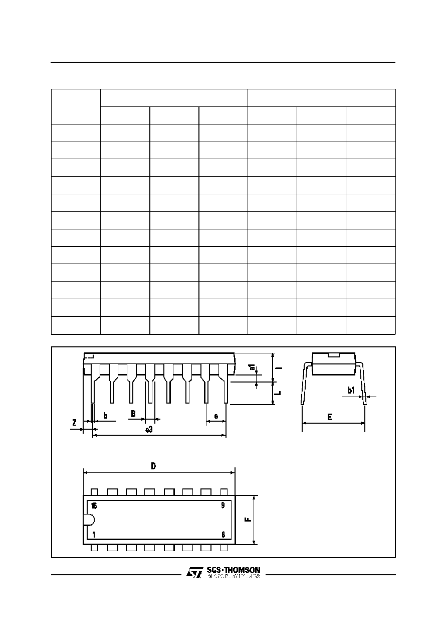
DIP16 PACKAGE MECHANICAL DATA
DIM.
mm
inch
MIN.
TYP.
MAX.
MIN.
TYP.
MAX.
a1
0.51
0.020
B
0.77
1.65
0.030
0.065
b
0.5
0.020
b1
0.25
0.010
D
20
0.787
E
8.5
0.335
e
2.54
0.100
e3
17.78
0.700
F
7.1
0.280
I
5.1
0.201
L
3.3
0.130
Z
1.27
0.050
LS256
7/8

Information furnished is believed to be accurate and reliable. However, SGS-THOMSON Microelectronics assumes no responsibility for
the consequences of use of such information nor for any infringement of patents or other rig hts of third parties which may result from its
use. No license is granted by implication or otherwise under any patent or patent rights of SGS-THOMSON Microelectronics. Specification
mentioned in this publication are subject to change without notice. This publication supersedes and replaces all information previously
supplied. SGS-THOMSON Microelectronics products are not authorized for use as critical components in life support devices or systems
without express written approval of SGS-THOMSON Microelectronics.
©
1996 SGS-THOMSON Microelectronics ≠ Printed in Italy ≠ All Rights Reserved
SGS-THOMSON Microelectronics GROUP OF COMPANIES
Australia - Brazil - Canada - China - France - Germany - Hong Kong - Italy - Japan - Korea - Malaysia - Malta - Morocco -
The Netherlands -Singapore - Spain - Sweden - Switzerland - Taiwan - Thailand - United Kingdom - U.S.A.
LS256
8/8