LS404
HIGH PERFORMANCE
QUAD OPERATIONAL AMPLIFIERS
December 1997
.
SINGLE OR SPLIT SUPPLY OPERATION
.
LOW POWER CONSUMPTION
.
SHORT CIRCUIT PROTECTION
.
LOW DISTORTION, LOW NOISE
.
HIGH GAIN-BANDWIDTH PRODUCT
.
HIGH CHANNEL SEPARATION
Inve rting Input 2
Non-inve rting Input 2
Non-inve rting Input 1
CC
V
-
C C
V
1
2
3
4
8
5
6
7
9
10
11
12
13
14
+
O utput 3
O utput 4
Non-inverting Inp ut 4
Inverting Inp ut 4
Non-inverting Inp ut 3
Inverting Inp ut 3
-
+
-
+
-
+
-
+
Output 1
Inve rting Input 1
Output 2
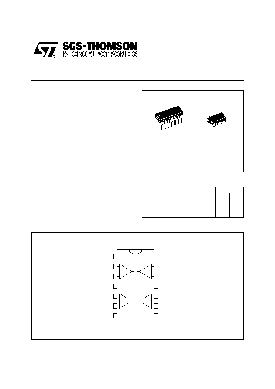
PIN CONNECTIONS (top view)
ORDER CODES
Part Number
Temperature Range
Package
N
D
LS404C
0
o
C, +70
o
C
�
�
LS404I
-40
o
C, +105
o
C
�
�
LS404M
-55
o
C, +125
o
C
�
�
N
DIP14
(Plastic Package)
D
SO14
(Plastic Micropackage)
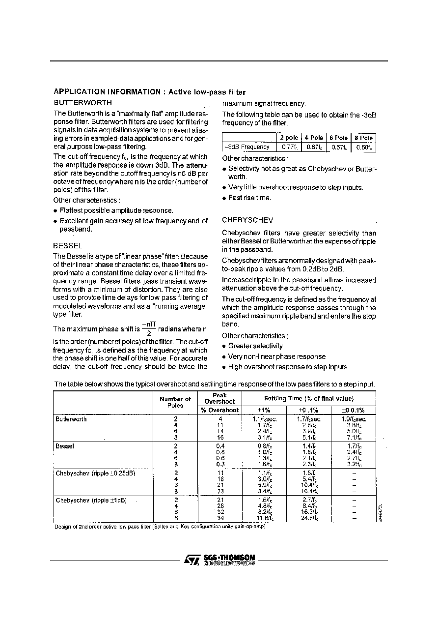
DESCRIPTION
The LS404 is a high performance quad operational
amplifier with frequency and phase compensation
built into the chip. The internal phase compensation
allows stable operation as voltage follower in spite
of its high Gain-Bandwidth Product.
The circuit presents very stable electrical charac-
teristics over the entire supply voltage range, and
it particularly intended for professional and telecom
applications (active filters, etc).
The patented input stage circuit allows small input
signal swings below the negative supply voltage
and prevents phase inversion when the inputs are
over drivers.
1/12
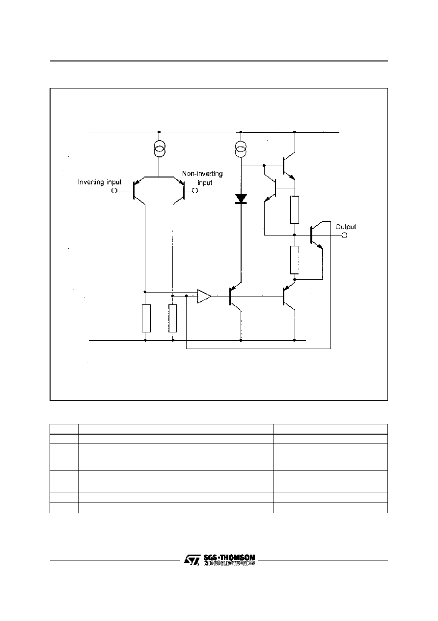
SCHEMATIC DIAGRAM (1/4 LS404)
ABSOLUTE MAXIMUM RATINGS
Symbol
Parameter
Value
Unit
V
CC
Supply Voltage
�
18
V
V
i
Input Voltage
(positive)
(negative)
+V
CC
-V
CC
- 0.5
V
V
id
Differential Input Voltage
�
(V
CC
- 1)
T
oper
Operating Temperature Range
LS404C
LS404I
LS404M
0 to +70
-40 to +105
-55 to +125
o
C
P
tot
Power Dissipation at T
amb
= 70
o
C
400
mW
T
stg
Storage Temperature
-65 to 150
o
C
LS404
2/12
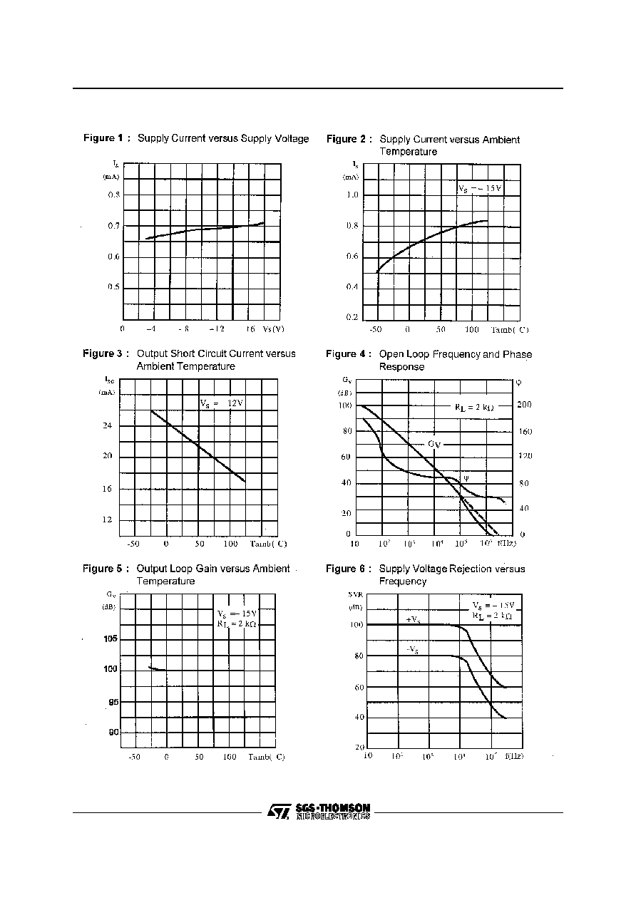
ELECTRICAL CHARACTERISTICS (V
CC
=
�
15V, T
amb
= 25
o
C, unless otherwise specified)
Symbol
Parameter
Test Conditions
LS404I - LM401M
LS404C
Unit
Min.
Typ.
Max.
Min.
Typ.
Max.
I
CC
Supply Current
1.3
2
1.5
3
mA
I
ib
Input Bias Current
50
200
100
300
nA
R
i
Input Resistance
f = 1kHz
1
1
M
V
io
Input Offset Voltage
R
s
10k
0.7
2.5
0.5
5
mV
DV
io
Input Offset Voltage Drift
R
s
10k
T
min
. < T
op
< T
max
.
5
5
�
V/
o
C
I
io
Input Offset Current
10
40
20
80
nA
DI
io
Input Offset Current Drift
T
min
. < T
op
< T
max
.
0.08
0.1
nA
�
C
I
os
Output Short Circuit Current
23
23
mA
A
vd
Large Signal Voltage Gain
R
L
= 2k
V
CC
=
�
15V
V
CC
=
�
4V
90
100
95
86
100
95
dB
GBP
Gain-Bandwidth Product
f = 100kHz R
L
= 2k
C
L
= 100pF
1.8
3
1.5
2.5
MHz
e
n
Equivalent Input Noise Voltage
f = 1kHz
R
s
= 50
R
s
= 1k
R
s
= 10k
8
10
18
15
10
12
20
nV
Hz
THD
Total Harmonic Distortion
Unity Gain
R
L
= 2k
, V
o
= 2V
pp
f = 1kHz
f = 20kHz
0.01
0.03
0.4
0.01
0.03
%
�
V
opp
Output Voltage Swing
R
L
= 2k
V
CC
=
�
15V
V
CC
=
�
4V
�
13
�
3
�
13
�
3
V
V
opp
Large Signal Voltage Swing
f = 10kHz R
L
= 10k
R
L
= 1k
22
20
22
20
V
PP
SR
Slew Rate
Unity Gain, R
L
= 2k
0.8
1.5
1
V/
�
s
CMR
Common Mode Rejection Ratio
V
ic
= 10V
90
94
80
90
dB
SVR
Supply Voltage Rejection Ratio
V
ic
= 1V
f = 100Hz
90
94
86
90
dB
V
O1
/V
O2
Channel Separation
f = 1kHz
100
120
120
dB
LS404
3/12
LS404
4/12
LS404
5/12
LS404
6/12
LS404
7/12
LS404
8/12
LS404
9/12
LS404
10/12
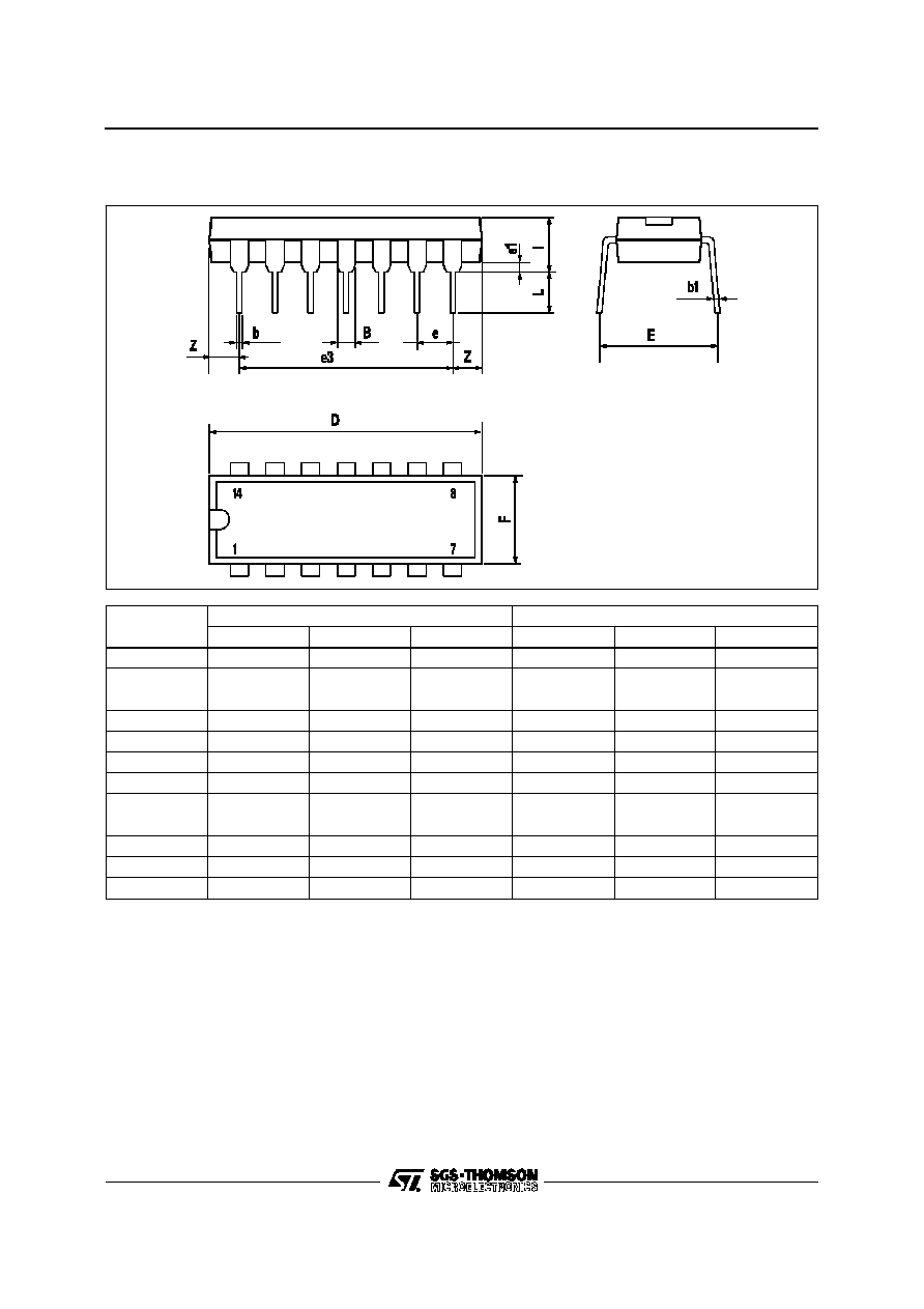
PACKAGE MECHANICAL DATA
14 PINS - PLASTIC DIP
Dim.
Millimeters
Inches
Min.
Typ.
Max.
Min.
Typ.
Max.
a1
0.51
0.020
B
1.39
1.65
0.055
0.065
b
0.5
0.020
b1
0.25
0.010
D
20
0.787
E
8.5
0.335
e
2.54
0.100
e3
15.24
0.600
F
7.1
0.280
i
5.1
0.201
L
3.3
0.130
Z
1.27
2.54
0.050
0.100
LS404
11/12
Information furnished is believed to be accurate and reliable. However, SGS-THOMSON Microelectronics assumes no responsibility
for the consequences of use of such information nor for any infringement of patents or other rights of third parties which may result
from its use. No license is granted by implication or otherwise under any patent or patent rights of SGS-THOMSON Microelectronics.
Specifications mentioned in this publication are subject to change without noti ce. This publication supersedes and replaces all
information previously supplied. SGS-THOMSON Microelectronics products are not authorized for use as critical components in life
support devices or systems without express written approval of SGS-THOMSON Microelectronics.
�
1997 SGS-THOMSON Microelectronics � Printed in Italy � All Rights Reserved
SGS-THOMSON Microelectronics GROUP OF COMPANIES
Australia - Brazil - Canada - China - France - Germany - Italy - Japan - Korea - Malaysia - Malta - Morocco
The Netherlands - Singapore - Spain - Sweden - Switzerland - Taiwan - Thailand - United Kingdom - U.S.A.
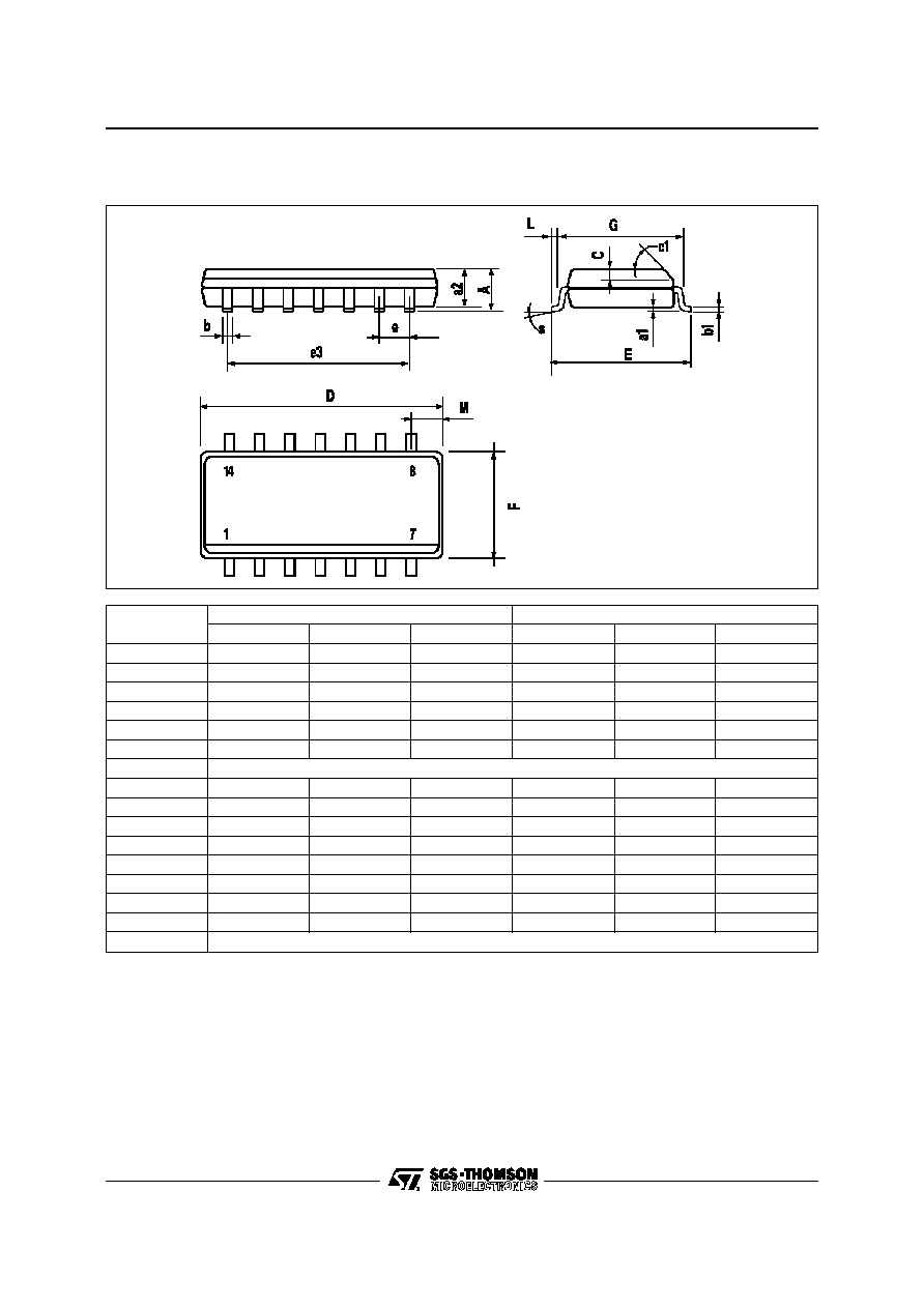
PACKAGE MECHANICAL DATA
14 PINS - PLASTIC MICROPACKAGE (SO)
Dim.
Millimeters
Inches
Min.
Typ.
Max.
Min.
Typ.
Max.
A
1.75
0.069
a1
0.1
0.2
0.004
0.008
a2
1.6
0.063
b
0.35
0.46
0.014
0.018
b1
0.19
0.25
0.007
0.010
C
0.5
0.020
c1
45
o
(typ.)
D
8.55
8.75
0.336
0.334
E
5.8
6.2
0.228
0.244
e
1.27
0.050
e3
7.62
0.300
F
3.8
4.0
0.150
0.157
G
4.6
5.3
0.181
0.208
L
0.5
1.27
0.020
0.050
M
0.68
0.027
S
8
o
(max.)
LS404
12/12