 | –≠–ª–µ–∫—Ç—Ä–æ–Ω–Ω—ã–π –∫–æ–º–ø–æ–Ω–µ–Ω—Ç: LS5060B | –°–∫–∞—á–∞—Ç—å:  PDF PDF  ZIP ZIP |
LS5018B
LS5060B/LS5120B
Æ
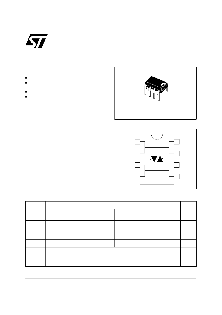
DIL8
TRISIL
TM
BIDIRECTIONAL CROWBAR PROTECTION.
BREAKDOWN VOLTAGES RANGE:
18V, 60V and 120V.
HOLDING CURRENT = 200mA min.
HIGH SURGE CURRENT CAPABILITY
I
PP
= 100A
10/1000
µ
s
FEATURES
The LS50xxB series has been designed to protect
telecommunication equipment against lightning
and transients induced by AC power lines.
Its high surge current capability makes the
LS50xxB a reliable protection device for very ex-
posed equipment, or when series resistors are
very low.
DESCRIPTION
CCITT K17 - K20
10/700
µ
s
1.5 kV
5/310
µ
s
38 A
VDE 0433
10/700
µ
s
2 kV
5/200
µ
s
50 A
CNET
0.5/700
µ
s
1.5 kV
0.2/310
µ
s
38 A
COMPLIES WITH THE FOLLOWING STANDARDS:
1
2
3
4
5
6
7
8
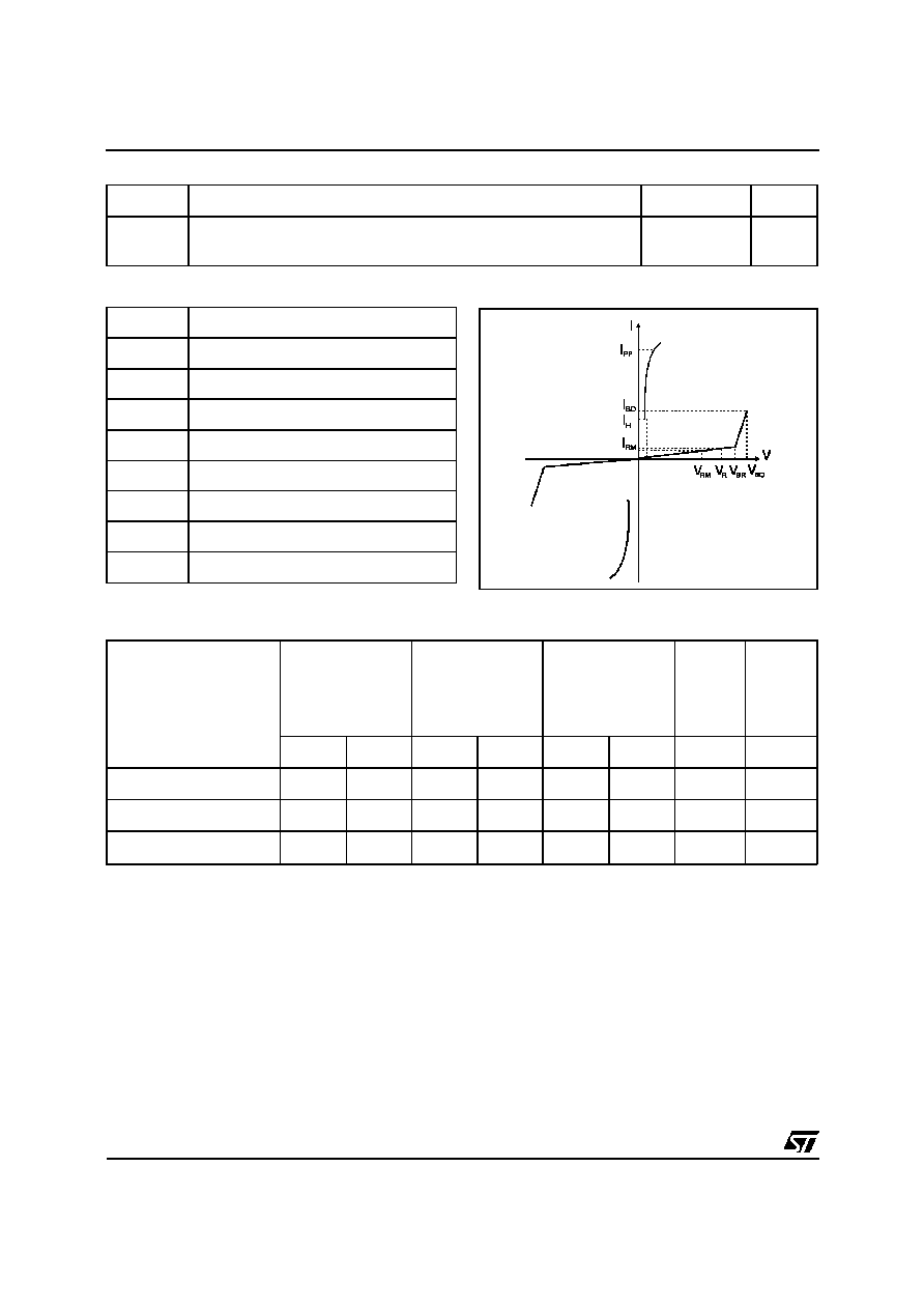
SCHEMATIC DIAGRAM
Symbol
Parameter
Value
Unit
I
PP
Peak pulse current
10/1000
µ
s
8/20
µ
s
100
250
A
I
TSM
Non repetitive surge peak on-state
current
tp = 20 ms
50
A
dI/dt
Critical rate of rise of on-state current
Non repetitive
100
A/
µ
s
dV/dt
Critical rate of rise of off-state voltage
V
RM
5
kV/
µ
s
T
stg
T
j
Storage and operating junction temperature range
- 40 to + 150
150
∞
C
∞
C
T
L
Maximum lead temperature for soldering during 10s
230
∞
C
ABSOLUTE MAXIMUM RATINGS (T
amb
=25
∞
C)
September 1998 Ed : 3A
1/5
Symbol
Parameter
I
RM
Leakage current at stand-offvoltage
V
RM
Stand-off voltage
V
BR
Breakdown voltage
V
BO
Breakover voltage
I
H
Holding current
I
BO
Breakover current
I
PP
Peak pulse current
C
Capacitance
ELECTRICAL CHARACTERISTICS (T
amb
=25
∞
C)
Type
I
RM
@ V
RM
V
BR
@ I
R
V
BO
@ I
BO
I
H
C
max.
min.
max.
typ.
min.
max.
note 1
note 2
note 3
µ
A
V
V
mA
V
mA
mA
pF
LS5018B
5
16
17
1
22
1300
200
150
LS5060B
10
50
60
1
85
1000
200
150
LS5120B
20
100
120
1
180
1250
250
150
Note 1 : Measured at 50Hz (1 cycle)
Note 2 : See test circuit
Note 3 : V
R
= 5 V, F = 1MHz.
Symbol
Parameter
Value
Unit
R
th
(j-a)
Junction to ambient on printed circuit with recommended pad
layout
80
∞
C/W
THERMAL RESISTANCE
LS5018B/LS5060B/LS5120B
2/5
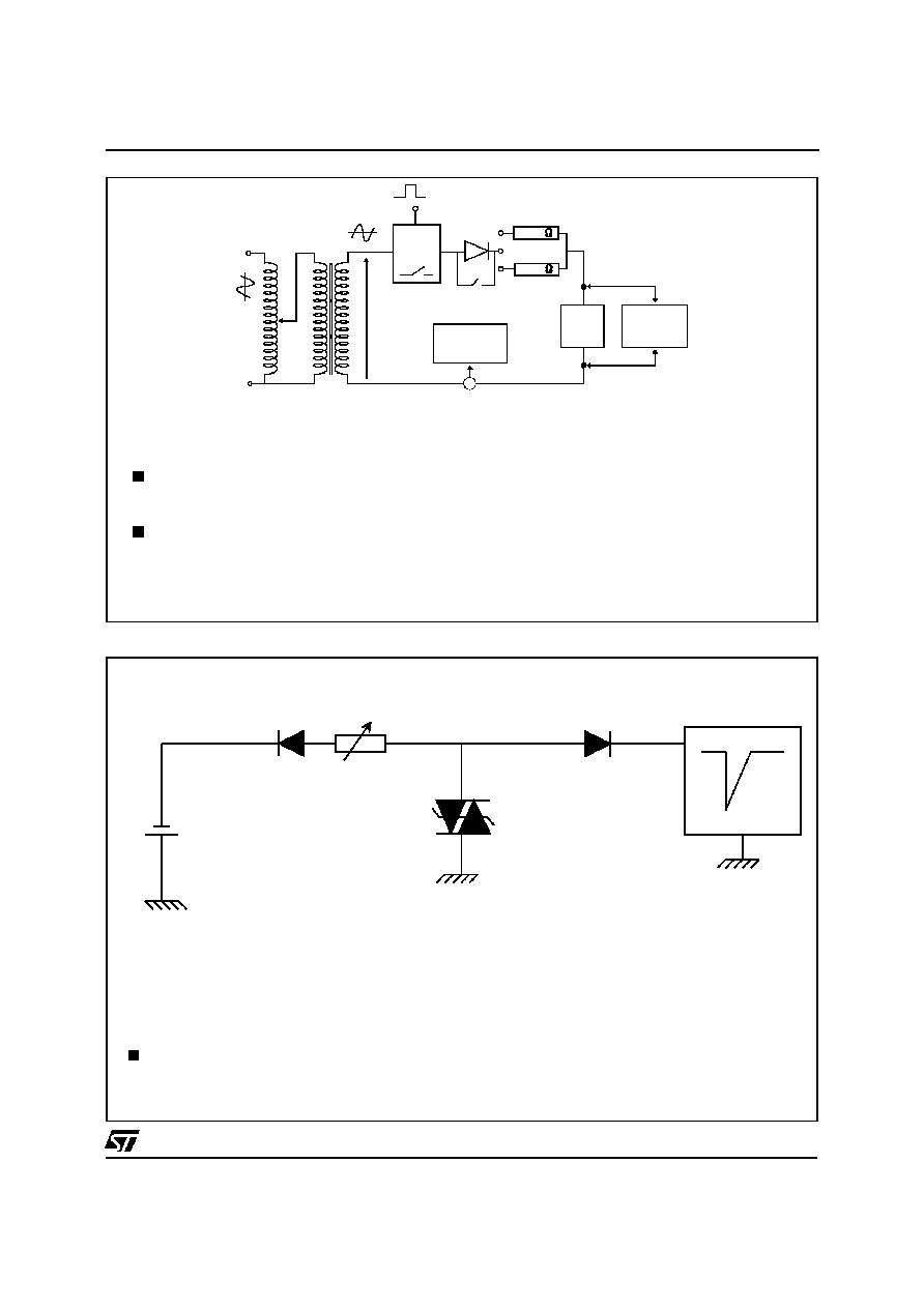
TEST CIRCUIT 1 FOR I
BO
and V
BO
parameters:
TEST PROCEDURE :
Pulse Test duration (tp = 20ms):
- For Bidirectional devices = Switch K is closed
- For Unidirectional devices = Switch K is open.
V
OUT
Selection
- Device with V
BO
<
200 Volt
- V
OUT
= 250 V
RMS
, R
1
= 140
.
- Device with V
BO
200 Volt
- V
OUT
= 480 V
RMS
, R
2
= 240
.
TEST CIRCUIT 2 for I
H
parameter.
This is a GO-NOGO Test which allows to confirm the holding current (I
H
) level in a functional
test circuit.
TEST PROCEDURE :
1) Adjust the current level at the I
H
value by short circuiting the AK of the D.U.T.
2) Fire the D.U.T with a surge Current : Ipp = 10A , 10/1000
µ
s.
3) The D.U.T will come back off-state within 50 ms max.
R
- V
P
V
BAT
= - 48 V
Surge generator
D.U.T.
220V
static
relay.
R1
R2
240
140
D.U.T
VBO
measure
IBO
measure
tp = 20ms
K
Transformer
220V/800V
5A
Auto
Transformer
220V/2A
Vout
LS5018B/LS5060B/LS5120B
3/5
1E-2
1E-1
1E+0
1E+1
1E+2
1E+3
I
TSM
(A)
0
10
20
30
40
50
60
70
F=50Hz
Tj initial=25
∞
C
t(s)
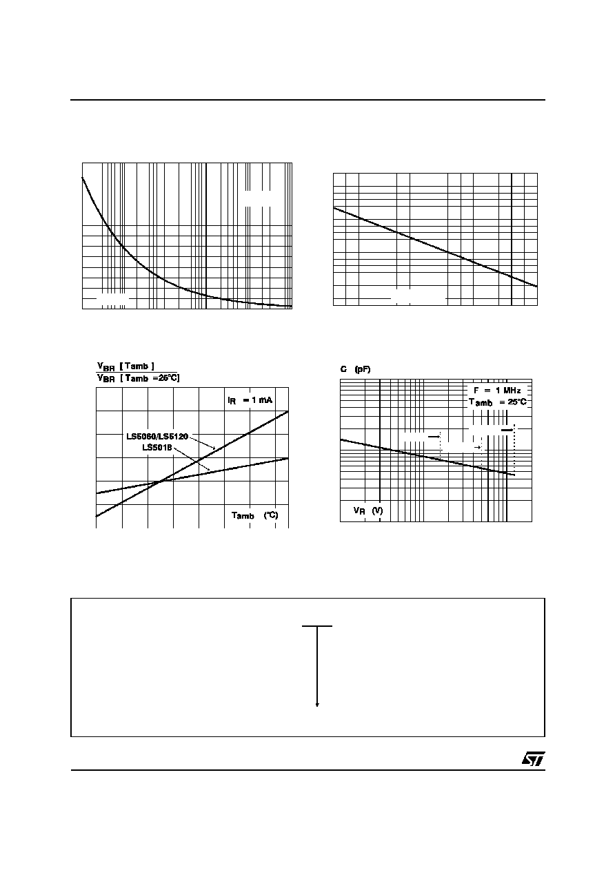
Figure 1 : Non repetitive surge peak current
versus overload duration
0.98
0.96
1.00
1.02
1.04
1.06
1.08
0
10
20
30
40
50
60
70
Figure 3 : Relative variation of breakdown voltage
versus ambient temperature.
1
10
100
200
10
100
1000
LS5018
LS5060
LS5120
Figure 4 : Junction capacitance versus reverse
applied voltage.
-40
-20
0
20
40
60
80
100
120
0.0
0.2
0.4
0.6
0.8
1.0
1.2
1.4
1.6
1.8
2.0
IH[Tj] / IH[Tj=25
∞
C]
Tamb (
∞
C)
Figure 2 : Relative variation of holding current
versus junction temperature.
ORDER CODE
LS5
018
B
VOLTAGE
LS5018B/LS5060B/LS5120B
4/5
Information furnished is believed to be accurate and reliable. However, STMicroelectronics assumes no responsIbility for the consequences of
use of such information nor for any infringement of patents or other rights of third parties which may result from its use. No license is granted by
implication or otherwise under any patent or patent rights of STMicroelectronics. Specifications mentioned in this publication are subject to
change without notice. This publication supersedes and replaces all information previously supplied.
STMicroelectronics products are not authorized for use as critical components in life support devices or systems without express written ap-
proval of STMicroelectronics.
The ST logo is a registered trademark of STMicroelectronics
©
1998 STMicroelectronics - Printed in Italy - All rights reserved.
STMicroelectronics GROUP OF COMPANIES
Australia - Brazil - Canada - China - France - Germany - Italy - Japan - Korea - Malaysia - Malta - Mexico - Morocco -
The Netherlands Singapore - Spain - Sweden - Switzerland - Taiwan - Thailand - United Kingdom - U.S.A.
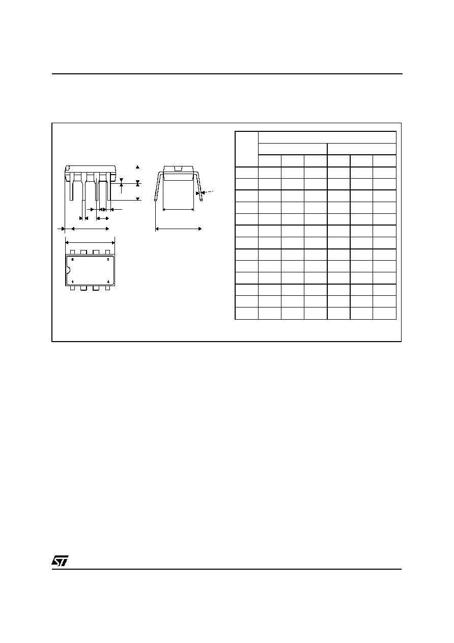
PACKAGE MECHANICAL DATA
DIL 8 Plastic
MARKING :
Logo, Date Code,part Number.
Packaging
: Products supplied in antistatic tubes.
W
eight : 0.59g
REF.
DIMENSIONS
Millimetres
Inches
Min.
Typ. Max. Min.
Typ. Max.
a1
0.70
0.027
B
1.39
1.65 0.055
0.065
B1
0.91
1.04 0.036
0.041
b
0.5
0.020
b1
0.38
0.50 0.015
0.020
D
9.80
0.385
E
8.8
0.346
e
2.54
0.100
e3
7.62
0.300
F
7.1
0.280
I
4.8
0.189
L
3.3
0.130
Z
0.44
1.60 0.017
0.063
8
1
5
4
E
D
F
b1
b
e3
e
Z
B
B1
I
L
a1
LS5018B/LS5060B/LS5120B
5/5