Äîêóìåíòàöèÿ è îïèñàíèÿ www.docs.chipfind.ru
1/26
December 2004
M36W0R5020T0
M36W0R5020B0
32 Mbit (2Mb x16, Multiple Bank, Burst) Flash Memory
and 4 Mbit SRAM, 1.8V Supply Multi-Chip Package
FEATURES SUMMARY
MULTI-CHIP PACKAGE
1 die of 32 Mbit (2Mb x 16) Flash Memory
1 die of 4 Mbit (256Kb x16) SRAM
SUPPLY VOLTAGE
V
DDF
= V
DDQ
= V
DDS
= 1.7 to 1.95V
LOW POWER CONSUMPTION
ELECTRONIC SIGNATURE
Manufacturer Code: 20h
Device Code (Top Flash Configuration):
8814h
Device Code (Bottom Flash
Configuration): 8815h
PACKAGE
Compliant with Lead-Free Soldering
Processes
Lead-Free Versions
FLASH MEMORY
PROGRAMMING TIME
8µs by Word typical for Fast Factory
Program
Double/Quadruple Word Program option
Enhanced Factory Program options
MEMORY BLOCKS
Multiple Bank Memory Array: 4 Mbit
Banks
Parameter Blocks (Top or Bottom
location)
SYNCHRONOUS / ASYNCHRONOUS READ
Synchronous Burst Read mode: 66MHz
Asynchronous/ Synchronous Page Read
mode
Random Access: 70ns
DUAL OPERATIONS
Program Erase in one Bank while Read in
others
No delay between Read and Write
operations
Figure 1. Package
BLOCK LOCKING
All blocks locked at Power-up
Any combination of blocks can be locked
WP
F
for Block Lock-Down
SECURITY
128-bit user programmable OTP cells
64-bit unique device number
COMMON FLASH INTERFACE (CFI)
100,000 PROGRAM/ERASE CYCLES per
BLOCK
SRAM
ACCESS TIME: 70ns
LOW V
DDS
DATA RETENTION: 1.0V
POWER DOWN FEATURES USING TWO
CHIP ENABLE INPUTS
FBGA
Stacked TFBGA88
(ZAQ)

M36W0R5020T0, M36W0R5020B0
2/26
TABLE OF CONTENTS
FEATURES SUMMARY . . . . . . . . . . . . . . . . . . . . . . . . . . . . . . . . . . . . . . . . . . . . . . . . . . . . . . . . . . . . . 1
FLASH MEMORY . . . . . . . . . . . . . . . . . . . . . . . . . . . . . . . . . . . . . . . . . . . . . . . . . . . . . . . . . . . . . . . 1
Figure 1. Package. . . . . . . . . . . . . . . . . . . . . . . . . . . . . . . . . . . . . . . . . . . . . . . . . . . . . . . . . . . . . . . 1
SRAM . . . . . . . . . . . . . . . . . . . . . . . . . . . . . . . . . . . . . . . . . . . . . . . . . . . . . . . . . . . . . . . . . . . . . . . . 1
SUMMARY DESCRIPTION . . . . . . . . . . . . . . . . . . . . . . . . . . . . . . . . . . . . . . . . . . . . . . . . . . . . . . . . . . . 4
Figure 2. Logic Diagram . . . . . . . . . . . . . . . . . . . . . . . . . . . . . . . . . . . . . . . . . . . . . . . . . . . . . . . . . . 4
Table 1. Signal Names . . . . . . . . . . . . . . . . . . . . . . . . . . . . . . . . . . . . . . . . . . . . . . . . . . . . . . . . . . 4
Figure 3. TFBGA Connections (Top view through package) . . . . . . . . . . . . . . . . . . . . . . . . . . . . . . 5
SIGNAL DESCRIPTIONS . . . . . . . . . . . . . . . . . . . . . . . . . . . . . . . . . . . . . . . . . . . . . . . . . . . . . . . . . . . . 6
Address Inputs (A0-A20). . . . . . . . . . . . . . . . . . . . . . . . . . . . . . . . . . . . . . . . . . . . . . . . . . . . . . . . . . 6
Data Input/Output (DQ0-DQ15). . . . . . . . . . . . . . . . . . . . . . . . . . . . . . . . . . . . . . . . . . . . . . . . . . . . . 6
Flash Chip Enable (E
F
).. . . . . . . . . . . . . . . . . . . . . . . . . . . . . . . . . . . . . . . . . . . . . . . . . . . . . . . . . . . 6
Flash Output Enable (G
F
). . . . . . . . . . . . . . . . . . . . . . . . . . . . . . . . . . . . . . . . . . . . . . . . . . . . . . . . . . 6
Flash Write Enable (W
F
).. . . . . . . . . . . . . . . . . . . . . . . . . . . . . . . . . . . . . . . . . . . . . . . . . . . . . . . . . . 6
Flash Write Protect (WP
F
). . . . . . . . . . . . . . . . . . . . . . . . . . . . . . . . . . . . . . . . . . . . . . . . . . . . . . . . . 6
Flash Reset (RP
F
). . . . . . . . . . . . . . . . . . . . . . . . . . . . . . . . . . . . . . . . . . . . . . . . . . . . . . . . . . . . . . . 6
Flash Latch Enable (L
F
). . . . . . . . . . . . . . . . . . . . . . . . . . . . . . . . . . . . . . . . . . . . . . . . . . . . . . . . . . . 6
Flash Clock (K
F
). . . . . . . . . . . . . . . . . . . . . . . . . . . . . . . . . . . . . . . . . . . . . . . . . . . . . . . . . . . . . . . . . 6
Flash Wait (WAIT
F
).. . . . . . . . . . . . . . . . . . . . . . . . . . . . . . . . . . . . . . . . . . . . . . . . . . . . . . . . . . . . . . 6
SRAM Chip Enable inputs (E1
S
, E2
S
). . . . . . . . . . . . . . . . . . . . . . . . . . . . . . . . . . . . . . . . . . . . . . . . 6
SRAM Write Enable (W
S
). . . . . . . . . . . . . . . . . . . . . . . . . . . . . . . . . . . . . . . . . . . . . . . . . . . . . . . . . . 6
SRAM Output Enable (G
S
). . . . . . . . . . . . . . . . . . . . . . . . . . . . . . . . . . . . . . . . . . . . . . . . . . . . . . . . . 6
SRAM Upper Byte Enable (UB
S
). . . . . . . . . . . . . . . . . . . . . . . . . . . . . . . . . . . . . . . . . . . . . . . . . . . . 6
SRAM Lower Byte Enable (LB
S
). . . . . . . . . . . . . . . . . . . . . . . . . . . . . . . . . . . . . . . . . . . . . . . . . . . . 7
V
DDF
Supply Voltage . . . . . . . . . . . . . . . . . . . . . . . . . . . . . . . . . . . . . . . . . . . . . . . . . . . . . . . . . . . . . 7
V
DDS
Supply Voltage. . . . . . . . . . . . . . . . . . . . . . . . . . . . . . . . . . . . . . . . . . . . . . . . . . . . . . . . . . . . . 7
V
DDQ
Supply Voltage. . . . . . . . . . . . . . . . . . . . . . . . . . . . . . . . . . . . . . . . . . . . . . . . . . . . . . . . . . . . . 7
V
PPF
Program Supply Voltage. . . . . . . . . . . . . . . . . . . . . . . . . . . . . . . . . . . . . . . . . . . . . . . . . . . . . . 7
V
SS
Ground.. . . . . . . . . . . . . . . . . . . . . . . . . . . . . . . . . . . . . . . . . . . . . . . . . . . . . . . . . . . . . . . . . . . . 7
FUNCTIONAL DESCRIPTION . . . . . . . . . . . . . . . . . . . . . . . . . . . . . . . . . . . . . . . . . . . . . . . . . . . . . . . . 8
Figure 4. Functional Block Diagram . . . . . . . . . . . . . . . . . . . . . . . . . . . . . . . . . . . . . . . . . . . . . . . . . 8
Table 2. Main Operating modes . . . . . . . . . . . . . . . . . . . . . . . . . . . . . . . . . . . . . . . . . . . . . . . . . . . 9
FLASH MEMORY COMPONENT . . . . . . . . . . . . . . . . . . . . . . . . . . . . . . . . . . . . . . . . . . . . . . . . . . . . . 10
SRAM COMPONENT . . . . . . . . . . . . . . . . . . . . . . . . . . . . . . . . . . . . . . . . . . . . . . . . . . . . . . . . . . . . . . 10
Figure 5. SRAM Block Diagram . . . . . . . . . . . . . . . . . . . . . . . . . . . . . . . . . . . . . . . . . . . . . . . . . . . 10
SRAM OPERATIONS . . . . . . . . . . . . . . . . . . . . . . . . . . . . . . . . . . . . . . . . . . . . . . . . . . . . . . . . . . . . . . 11
Read . . . . . . . . . . . . . . . . . . . . . . . . . . . . . . . . . . . . . . . . . . . . . . . . . . . . . . . . . . . . . . . . . . . . . . . . 11

3/26
M36W0R5020T0, M36W0R5020B0
Write . . . . . . . . . . . . . . . . . . . . . . . . . . . . . . . . . . . . . . . . . . . . . . . . . . . . . . . . . . . . . . . . . . . . . . . . 11
Standby/Power-Down . . . . . . . . . . . . . . . . . . . . . . . . . . . . . . . . . . . . . . . . . . . . . . . . . . . . . . . . . . . 11
Data Retention. . . . . . . . . . . . . . . . . . . . . . . . . . . . . . . . . . . . . . . . . . . . . . . . . . . . . . . . . . . . . . . . . 11
Output Disable . . . . . . . . . . . . . . . . . . . . . . . . . . . . . . . . . . . . . . . . . . . . . . . . . . . . . . . . . . . . . . . . . 11
MAXIMUM RATING. . . . . . . . . . . . . . . . . . . . . . . . . . . . . . . . . . . . . . . . . . . . . . . . . . . . . . . . . . . . . . . . 12
Table 3. Absolute Maximum Ratings . . . . . . . . . . . . . . . . . . . . . . . . . . . . . . . . . . . . . . . . . . . . . . . 12
DC AND AC PARAMETERS. . . . . . . . . . . . . . . . . . . . . . . . . . . . . . . . . . . . . . . . . . . . . . . . . . . . . . . . . 13
Table 4. Operating and AC Measurement Conditions . . . . . . . . . . . . . . . . . . . . . . . . . . . . . . . . . . 13
Figure 6. AC Measurement I/O Waveform . . . . . . . . . . . . . . . . . . . . . . . . . . . . . . . . . . . . . . . . . . . 13
Figure 7. AC Measurement Load Circuit. . . . . . . . . . . . . . . . . . . . . . . . . . . . . . . . . . . . . . . . . . . . . 13
Table 5. Device Capacitance. . . . . . . . . . . . . . . . . . . . . . . . . . . . . . . . . . . . . . . . . . . . . . . . . . . . . 13
Table 6. Flash Memory DC Characteristics - Currents . . . . . . . . . . . . . . . . . . . . . . . . . . . . . . . . . 14
Table 7. Flash Memory DC Characteristics - Voltages . . . . . . . . . . . . . . . . . . . . . . . . . . . . . . . . . 15
Table 8. SRAM DC Characteristics . . . . . . . . . . . . . . . . . . . . . . . . . . . . . . . . . . . . . . . . . . . . . . . . 15
Figure 8. SRAM Read Mode AC Waveforms, Address Controlled with UB
S
= LB
S
= V
IL
. . . . . . . 16
Figure 9. SRAM Read AC Waveforms, G
S
Controlled . . . . . . . . . . . . . . . . . . . . . . . . . . . . . . . . . . 16
Figure 10.SRAM Standby AC Waveforms. . . . . . . . . . . . . . . . . . . . . . . . . . . . . . . . . . . . . . . . . . . . 16
Table 9. SRAM Read AC Characteristics . . . . . . . . . . . . . . . . . . . . . . . . . . . . . . . . . . . . . . . . . . . 17
Figure 11.SRAM Write AC Waveforms, E1
S
or E2
S
Controlled . . . . . . . . . . . . . . . . . . . . . . . . . . . 18
Figure 12.SRAM Write AC Waveforms, W
S
Controlled, G
S
High during Write . . . . . . . . . . . . . . . . 19
Figure 13.SRAM Write AC Waveforms, W
S
Controlled with G
S
Low . . . . . . . . . . . . . . . . . . . . . . . 20
Figure 14.SRAM Write AC Waveform, UB
S
and LB
S
Controlled G
S
Low . . . . . . . . . . . . . . . . . . . . 20
Table 10. SRAM Write AC Characteristics . . . . . . . . . . . . . . . . . . . . . . . . . . . . . . . . . . . . . . . . . . . 21
Figure 15.SRAM Low V
DDS
Data Retention AC Waveforms, E1
S
or UB
S
/ LB
S
Controlled . . . . . . 22
Figure 16.SRAM Low V
DDS
Data Retention AC Waveforms, E2
S
Controlled . . . . . . . . . . . . . . . . . 22
Table 11. SRAM Low V
DDS
Data Retention Characteristic . . . . . . . . . . . . . . . . . . . . . . . . . . . . . . . 22
PACKAGE MECHANICAL . . . . . . . . . . . . . . . . . . . . . . . . . . . . . . . . . . . . . . . . . . . . . . . . . . . . . . . . . . 23
Figure 17. Stacked TFBGA88 8x10mm - 8x10 active ball array, 0.8mm pitch, Package Outline . . 23
Table 12. Stacked TFBGA88 8x10mm - 8x10 active ball array, 0.8mm pitch, Mechanical Data . . 23
PART NUMBERING . . . . . . . . . . . . . . . . . . . . . . . . . . . . . . . . . . . . . . . . . . . . . . . . . . . . . . . . . . . . . . . 24
Table 13. Ordering Information Scheme . . . . . . . . . . . . . . . . . . . . . . . . . . . . . . . . . . . . . . . . . . . . . 24
REVISION HISTORY . . . . . . . . . . . . . . . . . . . . . . . . . . . . . . . . . . . . . . . . . . . . . . . . . . . . . . . . . . . . . . . 25
Table 14. Document Revision History . . . . . . . . . . . . . . . . . . . . . . . . . . . . . . . . . . . . . . . . . . . . . . . 25
M36W0R5020T0, M36W0R5020B0
4/26
SUMMARY DESCRIPTION
The M36W0R5020T0 and M36W0R5020B0 com-
bine two memory devices in a Multi-Chip Package:
a 32-Mbit, Multiple Bank Flash memory, the
M58WR032FT/B
and a 4-Mbit SRAM.
Recommended operating conditions do not allow
more than one memory to be active at the same
time.
The memory is offered in a Stacked TFBGA88
(8 x 10mm, 8x10 ball array, 0.8mm pitch) pack-
age.
In addition to the standard version, the package is
also available in Lead-free version, in compliance
with JEDEC Std J-STD-020B, the ST ECOPACK
7191395 Specification, and the RoHS (Restriction
of Hazardous Substances) directive. All packages
are compliant with Lead-free soldering processes.
The memory supplied with all the bits erased (set
to `1').
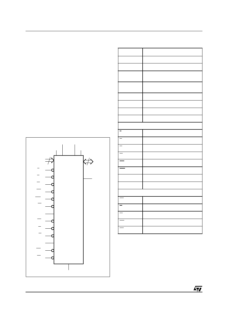
Figure 2. Logic Diagram
Table 1. Signal Names
Note: 1. A20-A18 are address inputs for the Flash memory com-
ponent only.
AI08754b
21
A0-A20
DQ0-DQ15
M36W0R5020T
M36W0R5020B
G
F
16
W
F
RP
F
WP
F
E1
S
G
S
W
S
UB
S
LB
S
VSS
V
DDF
V
PPF
V
DDS
WAIT
F
L
F
K
F
V
DDQ
E
F
E2
S
A0-A20
(1)
Address Inputs
DQ0-DQ15
Common Data Input/Output
V
DDF
Flash Memory Power Supply
V
DDQ
Common Flash and SRAM Power
Supply for I/O Buffers
V
PPF
Common Flash Optional Supply
Voltage for Fast Program and Erase
V
SS
Ground
V
DDS
SRAM Power Supply
NC
Not Connected Internally
DU
Do Not Use as Internally Connected
Flash Memory
L
F
Latch Enable input
E
F
Chip Enable input
G
F
Output Enable input
W
F
Write Enable input
RP
F
Reset input
WP
F
Write Protect input
K
F
Burst Clock
WAIT
F
Wait Data in Burst Mode
SRAM
E1
S
, E2
S
Chip Enable input
G
S
Output Enable input
W
S
Write Enable input
UB
S
Upper Byte Enable input
LB
S
Lower Byte Enable input
5/26
M36W0R5020T0, M36W0R5020B0
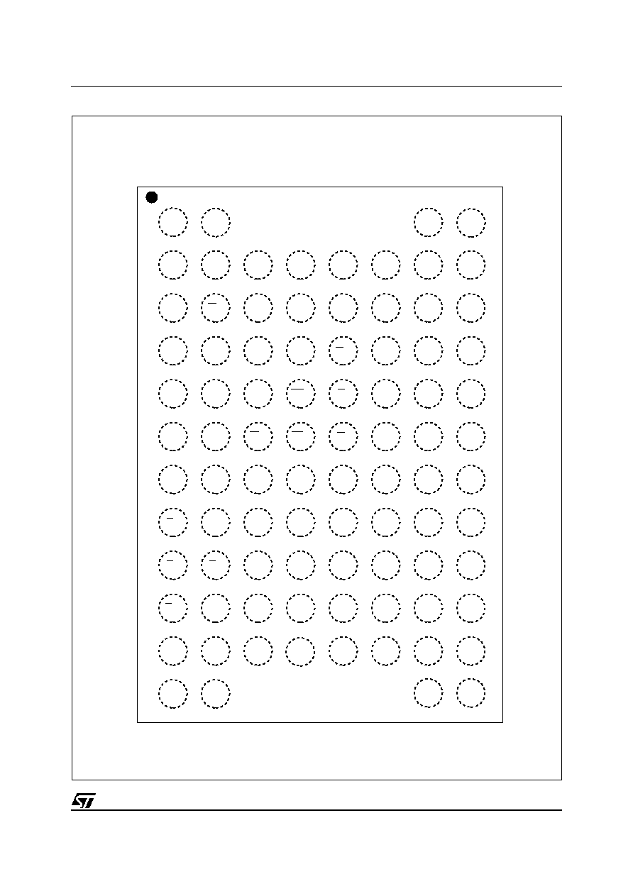
Figure 3. TFBGA Connections (Top view through package)
8
7
6
5
4
3
2
1
C
B
NC
KF
A4
A11
D
E
F
DU
DU
WF
VSS
A19
A18
NC
A5
A12
VSS
NC
LBS
A9
A3
A13
VPPF
NC
A17
A10
A20
A2
A15
LF
WPF
NC
A7
A14
A8
A1
A16
RPF
UBS
A6
WAITF
DQ13
A0
DQ5
DQ10
DQ2
DQ8
DQ7
DQ14
GS
DQ12
DQ3
DQ1
DQ0
DQ15
DQ6
DQ4
DQ11
DQ9
GF
VDDQ
EF
NC
VDDS
VSS
VSS
VSS
VSS
VSS
VDDF
VDDQ
VSS
DU
DU
DU
DU
DU
DU
A
G
H
J
K
AI08755
L
M
VDDF
NC
WS
E1S
NC
NC
NC
NC
NC
E2S
NC
NC
VDDQ
Document Outline