 | –≠–ª–µ–∫—Ç—Ä–æ–Ω–Ω—ã–π –∫–æ–º–ø–æ–Ω–µ–Ω—Ç: M39208NA | –°–∫–∞—á–∞—Ç—å:  PDF PDF  ZIP ZIP |
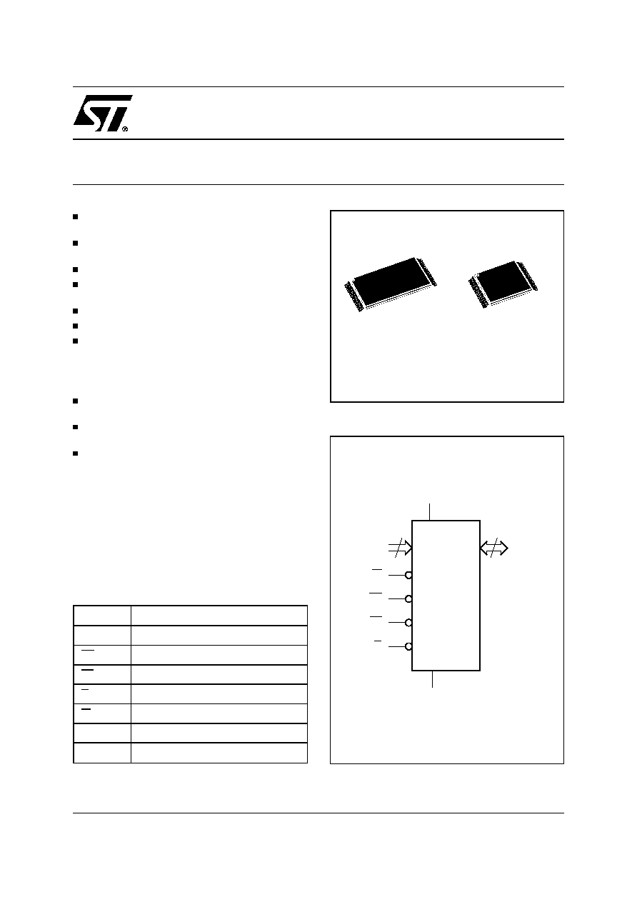
AI02589
18
A0-A17
EE
DQ0-DQ7
VCC
M39208
G
EF
VSS
8
W
Figure 1. Logic Diagram
M39208
Single Chip 2 Mbit Flash and 64 Kbit Parallel EEPROM Memory
PRELIMINARY DATA
2.7V to 3.6V SUPPLY VOLTAGE for
PROGRAM, ERASE and READ OPARATIONS
100ns ACCESS TIME
(Flash and EEPROM blocks)
WRITE, PROGRAM and ERASE STATUS BITS
CONCURRENT MODE (Read Flash while
writing to EEPROM)
100,000 ERASE/WRITE CYCLES
10 YEARS DATA RETENTION
LOW POWER CONSUMPTION
≠ Stand-by mode: 60
µ
A
≠ Automatic Stand-by mode
≠ Deep Power Down mode
64 bytes ONE TIME PROGRAMMABLE
MEMORY
STANDARD EPROM/OTP MEMORY
PACKAGE
EXTENDED TEMPERATURE RANGES
DESCRIPTION
The M39208 is a memory device combining Flash
and EEPROM into a single chip and using single
supply voltage. The memory is mapped in two
blocks: 2 Mbit of Flash memory and 64 Kbit of
EEPROM memory. Each space is independant for
writing, in concurrent mode the Flash Memory can
be read while the EEPROM is being written.
A0-A17
Address Inputs
DQ0-DQ7
Data Input / Outputs
EE
EEPROM Block Enable
EF
Flash Block Enable
G
Output Enable
W
Write Enable
V
CC
Supply Voltage
V
SS
Ground
Table 1. Signal Names
TSOP32 (NA)
8 x 20 mm
February 1999
1/30
This is preliminary information on a new product now in development or undergoing evaluation. Details are subject to change without notice.
TSOP32 (NB)
8 x 14 mm
Symbol
Parameter
Value
Unit
T
A
Ambient Operating Temperature
≠40 to 85
∞
C
T
BIAS
Temperature Under Bias
≠50 to 125
∞
C
T
STG
Storage Temperature
≠65 to 150
∞
C
V
IO
(2)
Input or Output Voltages
≠0.6 to 5
V
V
CC
Supply Voltage
≠0.6 to 5
V
V
A9
, V
G
, V
EF
(2)
A9, G, EF Voltage
≠0.6 to 13.5
V
Notes: 1. Except for the rating "Operating Temperature Range", stresses above those listed in the Table "Absolute Maximum Ratings"
may cause permanent damage to the device. These are stress ratings only and operation of the device at these or any other
conditions above those indicated in the Operating sections of this specification is not implied. Exposure to Absolute Maximum
Rating conditions for extended periods may affect device reliability. Refer also to the STMicroelectronics SURE Program and other
relevant quality documents.
2. Minimum Voltage may undershoot to ≠2V during transition and for less than 20ns.
Table 2. Absolute Maximum Ratings
(1)
An additional 64 bytes of EPROM are One Time
Programmable.
The M39208 EEPROM memory block may be writ-
ten by byte or by page of 64 bytes and the integrity
DESCRIPTION (Cont'd)
A3
A0
DQ0
A7
A4
A13
A11
DQ7
A14
VSS
G
DQ5
DQ1
DQ2
DQ3
DQ4
DQ6
A17
W
A16
A12
VCC
A15
AI02587
M39208
8
1
9
16
17
24
25
32
A9
A10
A8
EF
A6
A1
A5
A2
EE
Figure 2. TSOP Pin Connections
of the data can be secured with the help of the
Software Data Protection (SDP).
The M39208 Flash Memory block offers 4 sectors
of 64 Kbytes, each sector may be erased individu-
ally, and programmed Byte-by-Byte. Each sector
can be separately protected and unprotected
against program and erase. Sector erasure may be
suspended, while data is read from other sectors
of the Flash memory block (or EEPROM memory
block), and then resumed.
During a Program or Erase cycle in the Flash
memory block or during a Write in the EEPROM
memory block, the status of the M39208 internal
logic can be read on the Data Outputs DQ7,DQ6,
DQ5 and DQ3.
PIN DESCRIPTION
Address Inputs (A0-A17). The address inputs for
the memory array are latched during a write opera-
tion. A0-A12 access locations in the EEPROM
memory block A0-A17 access locations in the Flash
memory block. The memory block selected is given
by the state on the EE and EF inputs respectively.
When a specific voltage (V
ID
) is applied on the A9
address input, additional specific areas can be
accessed: Read the Manufacturer identifier, Read
the Flash block identifier, Read/Write the EEPROM
block identifier, Verify the Flash Sector Protection
Status.
Data Input/Output (DQ0-DQ7). A write operation
inputs one byte which is latched when EE (or EF)
and Write Enable W are driven active.
Data read is valid when one Chip Enable (Chip
Enable Flash or Chip Enable EEPROM) and Out-
put Enable are driven active. The output is high
2/30
M39208
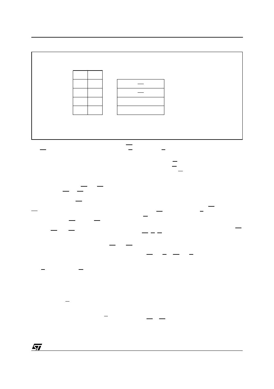
64K Bytes Block
AI02588
3FFFFh
2FFFFh
1FFFFh
0FFFFh
TOP
ADDRESS
30000h
20000h
10000h
00000h
BOTTOM
ADDRESS
64K Bytes Block
A17
1
1
A16
1
0
0
0
1
0
Figure 3. Flash Block Sectors
impedance when the chip is deselected (both EE
and EF driven high) or the outputs are disabled (G
driven high).
Read operations are used to output the contents
from the memory, the Manufacturer identifier, the
Flash Sector protection Status, the Flash block
Identifier, the EEPROM identifier or the OTP row
content.
Memory Block Enable (EE and EF). The Memory
Block Enable (EE or EF) activates the memory
control logic, input buffers, decoders and sense
amplifiers. When the EE input is driven high, the
EEPROM memory block is not selected; when the
EF input is driven high, the Flash memory block is
not selected. Attempts to access both EEPROM
and Flash blocks (EE low and EF low) are forbid-
den. Switching between the two memory block
enables (EE and EF) must not be made on the
same clock cycle, a delay of greater than t
EHFL
must
be inserted.
The M39208 is in standby when both EF and EE
are High (when no internal Erase or programming
is running). The power consumption is reduced to
the standby level and the outputs are in the high
impedance state, independent of the Output En-
able G or Write Enable W inputs.
After 150ns of inactivity and when the addresses
are driven at CMOS levels, the chip automatically
enters a pseudo standby mode where consumption
is reduced to the CMOS standby value, while the
outputs continue to drive the bus.
Output Enable (G). The Output Enable gates the
outputs through the data buffers during a read
operation. The data outputs are in the high imped-
ance state when the Output Enable G is High.
During Sector Protect and Sector Unprotect opera-
tions, the G input must be forced to V
ID
level (12V
+ 0.5V) (for Flash memory block only).
Write Enable (W). Addresses are latched on the
falling edge of W, and Data Inputs are latched on
the rising edge of W.
OPERATIONS
The M39208 memory is addressed through 18
inputs A0-A17 and provides data on eight Data
Inputs/Outputs DQ0-DQ7 with the help of four con-
trol lines: Chip Enable EEPROM (EE), Chip Enable
Flash (EF), Output Enable (E) and Write Enable
(W) inputs.
An operation is defined as the basic decoding of
the logic level applied to the control input pins (EF,
EE, G, W) and the specified voltages applied on
the relevant address pins. These operations are
detailed in Table 3.
Read. Both Chip Enable and Output Enable (that
is EF and G or EE and G) must be low in order to
read the output of the memory.
Read operations are used to output the contents
from the Flash or EEPROM block, the Manufac-
turer identifier, the Flash Sector protection Status,
the Flash block Identifier, the EEPROM identifier or
the OTP row content.
Notes:
≠ The Chip Enable input mainly provides power
control and should be used for device selection.
The Output Enable input should be used to gate
data onto the output in combination with active
EF or EE input signals.
≠ The data read depends on the previous instruc-
tion entered into the memory (see Table 4).
3/30
M39208
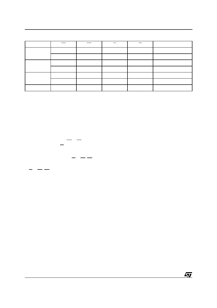
Operation
EF
EE
G
W
DQ0 - DQ7
Read
V
IL
V
IH
V
IL
V
IH
Read in Flash Block
V
IH
V
IL
V
IL
V
IH
Read in EEPROM Block
Write
V
IL
V
IH
V
IH
V
IL
Write in Flash Block
V
IH
V
IL
V
IH
V
IL
Write in EEPROM Block
Output Disable
V
IL
V
IH
V
IH
X
Hi-Z
V
IH
V
IL
V
IH
X
Hi-Z
Standby
V
IH
V
IH
X
X
Hi-Z
Note: X = V
IL
or V
IH
.
Table 3. Basic Operations
Write. A Write operation can be used for two goals:
≠ either write data in the EEPROM memory block
≠ or enter a sequence of bytes composing an
instruction.
The reader should note that Programming a Flash
byte is an instruction (see Instructions paragraph).
Writing data requires:
≠ the Chip Enable (either EE or EF) to be Low
≠ the Write Enable (W) to be Low with Output
Enable (G) High.
Addresses in Flash block (or EEPROM block) are
latched on the falling edge of W or EF (EE) which-
ever occurs last; the data to be written in Flash
block (EEPROM block) is latched on the rising edge
of W or EF (EE) whichever occurs first.
Specific Read and Write Operations. Device
specific data is accessed through operations de-
coding the V
ID
level applied on A9 (V
ID
= 12V +
0.5V) and the logic levels applied on address inputs
(A0, A1, A6). These specific operations are:
≠ Read the Manufacturer identifier
≠ Read the Device identifier
≠ Define the Flash Sector protection
≠ Read the EEPROM identifier
≠ Write the EEPROM identifier
Note: The OTP row (64 bytes) is accessed with a
specific software sequence detailed in the para-
graph "Write in OTP row".
Instructions
An instruction is defined as a sequence of specific
Write operations. Each received byte is sequen-
tially decoded (and not executed as standard Write
operations) and the instruction is executed when
the correct number of bytes are properly received
and the time between two consecutive bytes is
shorter than the time-out value.
The sequencing of any instruction must be followed
exactly, any invalid combination of instruction bytes
or time-out between two consecutive bytes will
reset the device logic into a Read memory state
(when addressing the Flash block) or directly de-
coded as a single operation when addressing the
EEPROM block.
The M39208 set of instructions includes:
≠ Program a byte in the Flash block
≠ Read a Flash sector protection status
≠ Erase instructions: Flash Sector Erase, Flash
Block Erase, Flash Sector Erase Suspend, Flash
Sector Erase Resume
≠ EEPROM power down
≠ Deep power down
≠ Set/Reset the EEPROM software write protec-
tion (SDP)
≠ OTP row access
≠ Reset and Return
≠ Read identifiers: read the manufacturer identi-
fier, Read the Flash block identifier
These instructions are detailed in Table 4.
For efficient decoding of the instruction, the two first
bytes of an instruction are the coded cycles and are
followed by a command byte or a confirmation byte.
The coded cycles consist of writing the data AAh at
address 5555h during the first cycle and data 55h
at address 2AAAh during the second cycle.
In the specific case of the Erase instruction, the
instruction expects confirmation by two additional
coded cycles.
4/30
M39208
Instruction
EE
EF
Cycle 1
Cycle 2
Cycle 3
Cycle 4
Cycle 5
Cycle 6
Cycle 7
Read Manufacturer
Identifier
(2)
1
0
AAh
@5555h
55h
@2AAAh
90h
@5555h
Read
Identifier
with
(A0,A1,A6)
at (0,0,0)
Read Flash
Identifier
(2)
1
0
AAh
@5555h
55h
@2AAAh
90h
@5555h
Read
identifier
with
(A0,A1,A6)
at (1,0,0)
Read OTP Row
0
1
AAh
@5555h
55h
@2AAAh
90h
@5555h
Read
byte 1
Read
byte 2
Read
byte N
Read Block
Protection Status
(2)
1
0
AAh
@5555h
55h
@2AAAh
90h
@5555h
Read
Identifier
with
(A0,A1,A6)
at (0,1,0)
Program a Flash Byte
1
0
AAh
@5555h
55h
@2AAAh
A0h
@5555h
Data
@address
Erase one Flash
Block
1
0
AAh
@5555h
55h
@2AAAh
80h
@5555h
AAh
@5555h
55h
@2AAAh
30h
@Sector
address
30h
@Sector
address
(3)
Erase the Whole Flash
1
0
AAh
@5555h
55h
@2AAAh
80h
@5555h
AAh
@5555h
55h
@2AAAh
10h
@5555h
Suspend Block Erase
1
0
B0h
@any
address
Resume Block Erase
1
0
30h
@any
address
EEPROM Power
Down
0
1
AAh
@5555h
55h
@2AAAh
30h
@5555h
Deep Power Down
1
0
20h
@5555h
SDP Enable
(EEPROM)
0
1
AAh
@5555h
55h
@2AAAh
A0h
@5555h
Write
byte 1
Write
byte 2
Write
byte N
SDP Disable
(EEPROM)
0
1
AAh
@5555h
55h
@2AAAh
80h
@5555h
AAh
@5555h
55h
@2AAAh
20h
@5555h
Write in OTP Row
0
1
AAh
@5555h
55h
@2AAAh
B0h
@5555h
Write
byte 1
Write
byte 2
Write
byte N
Return (from OTP
Read or EEPROM
Power Down)
0
1
F0h @
any
address
Reset
1
0
AAh
@5555h
55h
@2AAAh
F0h
@any
Address
Reset (short
instruction)
1
0
F0h
@any
address
Notes: 1. AAh @5555h means Write byte AAh at address 5555h.
2. This instruction can also be performed as a simple Read operation with A9=V
ID
(refer to READ chapter).
3. Additional blocks to be erased must be entered within 80
µ
s.
Table 4. Instructions
(1)
5/30
M39208