 | –≠–ª–µ–∫—Ç—Ä–æ–Ω–Ω—ã–π –∫–æ–º–ø–æ–Ω–µ–Ω—Ç: M39432NC | –°–∫–∞—á–∞—Ç—å:  PDF PDF  ZIP ZIP |
1/28
November 1999
M39432
Single Chip 4 Mbit Flash Memory and
256 Kbit Parallel EEPROM
s
Multiple Memories on a Single Chip:
≠ 4 Mbit Flash Memory (organised as 8 sectors)
≠ 256 Kbit EEPROM
≠ 64 Byte One Time Programmable Memory
s
CONCURRENT Mode (Read Flash while
writing to EEPROM)
s
WRITE, PROGRAM and ERASE Status Bits
s
2.7V to 3.6V Single Supply Voltage for
PROGRAM, ERASE and READ Operations
s
100 ns Access Time (Flash and EEPROM
blocks)
s
Low Power Consumption
≠ 60
µ
A Stand-by mode (maximum)
≠ Deep Power Down mode:
6
µ
A (maximum), 200 nA (typical)
s
Standard Flash Memory Package
s
100,000 Erase/Write Cycles (minimum)
s
10 Year Data Retention (minimum)
DESCRIPTION
The M39432 is a single supply voltage memory
device combining Flash memory and EEPROM on
a single chip. The memory is mapped in two
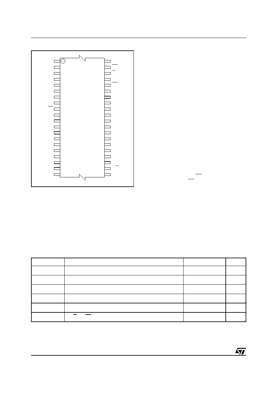
Figure 1. Logic Diagram
AI01946
19
A0-A18
EE
DQ0-DQ7
VCC
M39432
G
EF
VSS
8
W
R/B
Table 1. Signal Names
A0-A18
Address Inputs
DQ0-DQ7
Data Inputs / Outputs
EE
EEPROM Block Enable
EF
Flash Block Enable
G
Output Enable
W
Write Enable
R/B
Ready/Busy Output
V
CC
Supply Voltage
V
SS
Ground
TSOP40 (NC)
10 x 20 mm
M39432
2/28
blocks: 4 Mbit of Flash memory and 256 Kbit of
EEPROM. Each block operates independently
during a Write cycle: in concurrent mode, the
Flash Memory can be read while the EEPROM is
being written.
There is also a 64 byte row of OTP (one time
programmable) EPROM.
The M39432 EEPROM block may be written
bytewise or by a page at a time (up to 64 bytes).
The integrity of the data can be secured with the
help of the Software Data Protection (SDP).
The M39432 Flash Memory block offers 8 sectors,
each one 64 KByte in size. Each sector may be
erased individually, and programmed a byte at a
time. Each sector can be separately protected and
unprotected against Program and Erase. Sector
erasure may be suspended, while data is read
from other sectors of the Flash memory block (or
from the EEPROM block), and then resumed. The
Flash memory block is functionally compatible with
the M29W040 (4 Mbit Single Voltage Flash
Memory).
During a Program or Erase cycle in the Flash
memory or during a Write cycle in the EEPROM,
the status of the M39432 internal logic can be read
on the Data Output pins DQ7, DQ6, DQ5 and
DQ3.
SIGNAL DESCRIPTION
Address Inputs (A0-A18)
The address inputs for the memory array are
latched during a write operation. The EEPROM
block is selected by the EE input, and the Flash
memory block the EF input. A0-A14 access
locations in the EEPROM block; A0-A18 access
locations in the Flash memory block.
When V
ID
(as specified in Table 11) is applied on
the A9 address input, additional device-specific
information can be accessed:
≠ Read the Manufacturer identifier
≠ Read the Flash block identifier
≠ Read/Write the EEPROM block identifier
≠ Verify the Flash Sector Protection Status.
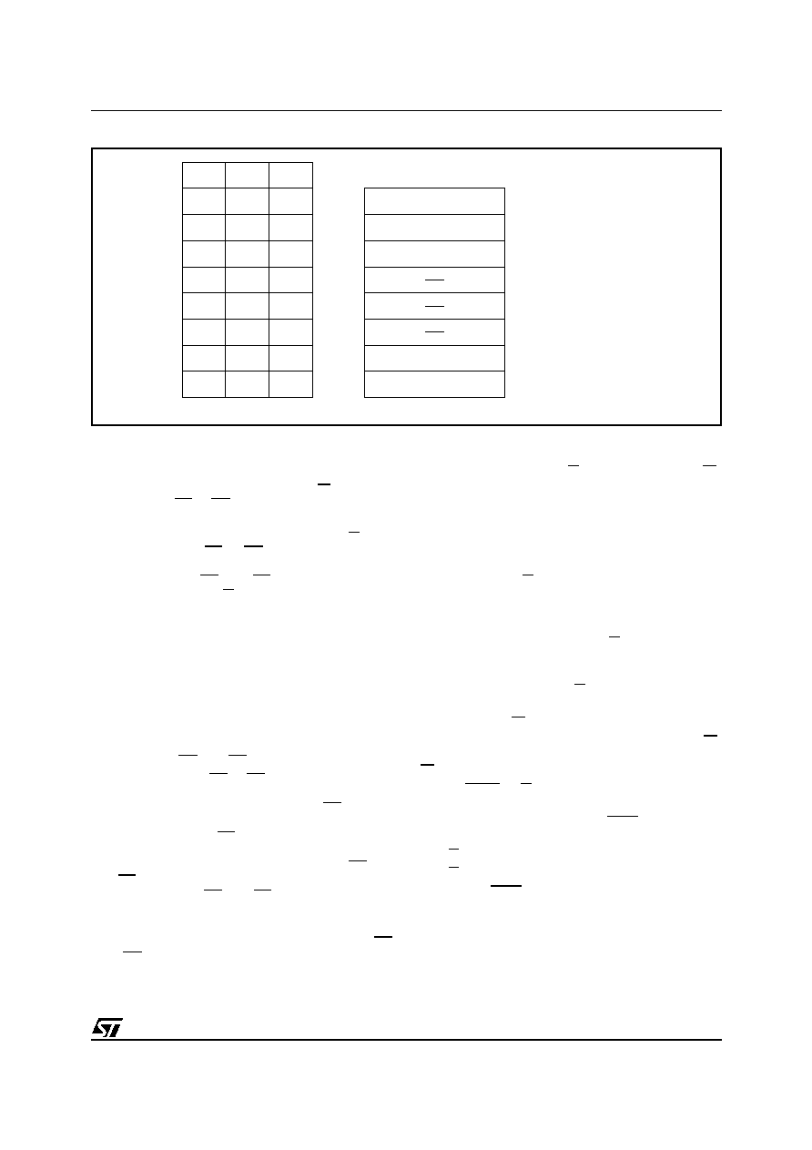
Figure 2. TSOP Connections
Note: 1. NC = Not Connected.
A3
A0
DQ0
A7
NC
R/B
A4
NC
A13
EE
A11
NC
DQ7
A14
NC
VSS
G
DQ5
DQ1
DQ2
DQ3
DQ4
DQ6
A17
W
A16
A12
A18
VCC
A15
AI01947
M39432
10
1
11
20
21
30
31
40
NC
A9
A10
A8
EF
A6
A1
A5
A2
NC
Table 2. Absolute Maximum Ratings
Note: 1. Stresses above those listed may cause permanent damage to the device. These are stress ratings only and operation of the device
at these or any other conditions above those indicated in the Operating sections of this specification is not implied. Exposure to
Absolute Maximum Rating conditions for extended periods may affect device reliability. Please see the STMicroelectronics SURE
Program and other relevant quality documents.
2. Minimum voltage may undershoot to ≠2 V, during transition and for less than 20 ns.
Symbol
Parameter
Value
Unit
T
A
Ambient Operating Temperature
≠40 to 85
∞C
T
BIAS
1
Temperature Under Bias
≠50 to 125
∞C
T
STG
1
Storage Temperature
≠65 to 150
∞C
V
IO
1,2
Input or Output Voltage (except A9)
≠0.6 to 7
V
V
CC
1
Supply Voltage
≠0.6 to 7
V
V
A9
, V
G
, V
EF
1,2
A9, G and EF Voltage
≠0.6 to 13.5
V
3/28
M39432
Data Input/Output (DQ0-DQ7)
During a Write operation, one data byte is latched
into the device when Write Enable (W) and one
Chip Enable (EF or EE) are driven low.
During a Read operation, the output presented on
these pins is valid when Output Enable (G) and
one Chip Enable (EF or EE) are driven low. The
output is high impedance when the chip is
deselected (both EE and EF driven high) or the
outputs are disabled (G driven high).
Read operations are used to output:
≠ bytes in the Flash memory block
≠ bytes in the EEPROM block
≠ the Manufacturer Identifier
≠ the Flash Sector Protection Status
≠ the Flash Block Identifier
≠ the EEPROM Identifier
≠ the OTP row.
Chip Enable (EE and EF)
Each Chip Enable (EE or EF) causes the memory
control logic, input buffers, decoders and sense
amplifiers to be activated. When the EE input is
driven high, the EEPROM memory block is not
selected; when the EF input is driven high, the
Flash memory block is not selected. Attempts to
access both EEPROM and Flash blocks (EE low
and EF low) are forbidden. Switching between the
two chip enables (EE and EF) must not be made
on the same clock cycle, a delay of greater than
t
EHFL
must occur.
The M39432 is in stand-by mode when both EF
and EE are high (when no internal Erase or
programming cycle is running). The power
consumption is reduced to the stand-by level and
the outputs are held in the high state, independent
of the Output Enable (G) or Write Enable (W)
inputs.
After 150 ns of inactivity, and when the addresses
are driven at CMOS levels, the chip automatically
enters a pseudo-stand-by mode. Power
consumption is reduced to the CMOS stand-by
level, while the outputs continue to drive the bus.
Output Enable (G)
The Output Enable gates the outputs through the
data buffers during a Read operation. The data
outputs are left floating in their high impedance
state when the Output Enable (G) is high.
During Sector Protect (Figure 8) and Sector
Unprotect (Figure 9) operations (for the Flash
memory block only), the G input must be held at
V
ID
(as specified in Table 11).
Write Enable (W)
Addresses are latched on the falling edge of W,
and Data Inputs are latched on the rising edge of
W.
Ready/Busy (R/B)
When the EEPROM block is engaged in an
internal Write cycle, the Ready/Busy output shows
the status of the device:
≠ R/B is 0 when a Write cycle is in progress
≠ R/B is Hi-Z when no Write cycle is in progress
The Ready/Busy pin does not show the status of a
Program or Erase cycle in the Flash memory.
This pin can be used to show the status of the
EEPROM block, even when reading data (or
fetching instructions) from the Flash memory
block.
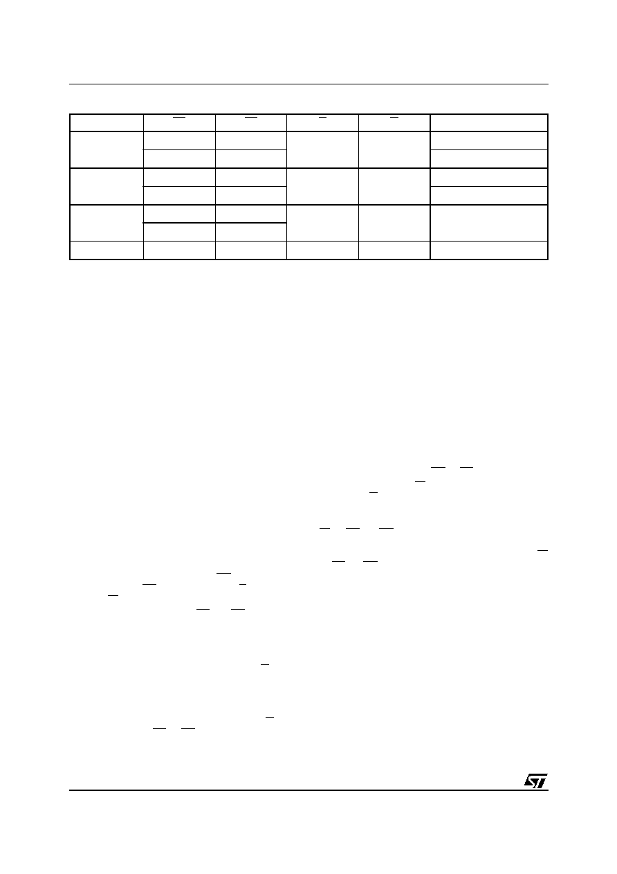
Figure 3. Flash Block Sectors
64K Bytes Block
AI01362B
7FFFFh
6FFFFh
5FFFFh
4FFFFh
3FFFFh
2FFFFh
1FFFFh
0FFFFh
TOP
ADDRESS
70000h
60000h
50000h
40000h
30000h
20000h
10000h
00000h
BOTTOM
ADDRESS
A18
1
1
64K Bytes Block
64K Bytes Block
64K Bytes Block
64K Bytes Block
A17
1
1
A16
1
0
1
1
0
0
1
0
0
0
1
1
1
0
0
0
1
0
0
0
M39432
4/28
This open drain output can be wire-ORed, using
an external pull-up resistor, when several M39xxx
devices are used together.
V
CC
Supply Voltage
The V
CC
Supply Voltage supplies the power for
the device. The M39432 cannot be written when
the V
CC
Supply Voltage is less than the Lockout
Voltage, V
LKO
. This prevents Bus Write operations
from accidentally damaging the data during power
up, power down and during power surges.
A 100 nF capacitor should be connected between
the V
CC
Supply Voltage pin and the V
SS
Ground
pin, to decouple the current surges from the power
supply. The PCB track widths must be sufficient to
carry the currents required during program and
erase operations.
V
SS
Ground
The V
SS
Ground is the reference for all voltage
measurements.
DEVICE OPERATION
The M39432 memory device is addressed via 19
inputs (A0-A18) and carries data on 8 Data Inputs/
Outputs (DQ0-DQ7). There are four other control
inputs: Chip Enable EEPROM (EE), Chip Enable
Flash Memory (EF), Output Enable (E) and Write
Enable (W).
The Chip Enable inputs (EF or EE) are used
mainly for power control (turning the chip on and
off) and for block selection (selecting the
EEPROM block or the Flash memory block). The
gating of data to the DQ0-DQ7 pins should be
controlled using the Output Enable input (G).
The permitted operating modes of the device are
listed in Table 3.
Read
For a Read operation, the Output Enable (G) and
one Chip Enable (EF or EE) must be driven low.
As noted on the previous page, Read operations
are used to read the contents of:
≠ bytes in the Flash memory block
≠ bytes in the EEPROM block
≠ the Manufacturer Identifier
≠ the Flash Sector Protection Status
≠ the Flash Block Identifier
≠ the EEPROM Identifier
≠ the OTP row.
The instruction sequences for selecting between
these areas is summarized in Table 4.
Write
Writing data requires:
≠ a Chip Enable (either EE or EF) to be low
≠ the Write Enable (W) to be low and the Output
Enable (G) to be high.
Addresses in the Flash memory block (or the
EEPROM block) are latched on the falling edge of
W or EF (or EE) whichever occurs the later. The
data to be written to the Flash memory block (or
EEPROM block) is latched on the rising edge of W
or EF (or EE) whichever occurs first.
The Write operation is used in two contexts:
≠ to write data to the EEPROM memory block
≠ to enter the sequence of bytes that makes up
one of the instructions shown in Table 4.
The programming of a byte of Flash memory
involves one of these instructions (as described in
the section entitled "Instructions" on this page).
Specific Read and Write Operations
Device specific information includes the following:
≠ Read the Manufacturer Identifier
≠ Read the Device Identifier
≠ Define the Flash Sector Protection
≠ Read the EEPROM Identifier
≠ Write the EEPROM Identifier
Table 3. Operations
Note: 1. X = V
IH
or V
IL
.
Operation
EF
EE
G
W
DQ0 - DQ7
Read
V
IL
V
IH
V
IL
V
IH
Read from Flash Block
V
IH
V
IL
Read from EEPROM Block
Write
V
IL
V
IH
V
IH
V
IL
Write to Flash Block
V
IH
V
IL
Write to EEPROM Block
Output Disable
V
IL
V
IH
V
IH
X
Hi-Z
V
IH
V
IL
Stand-by
V
IH
V
IH
X
X
Hi-Z
5/28
M39432
Table 4. Instructions
1
Note: 1. AAh @ 5555h means "Write the value AAh at the address 5555h".
2. This instruction can also be performed as a Verify operation with A9=V
ID
(please see the section entitled "Flash Sector Protection
and Unprotection" on page 18).
3. Addresses of additional sectors to be erased must be entered within a time-out of 80
µ
s of each other.
Instruction
EE
EF
Cycle 1
Cycle 2
Cycle 3
Cycle 4
Cycle 5
Cycle 6
Cycle 7
Read
Manufacturer
Identifier
2
1
0
AAh
@5555h
55h
@2AAAh
90h
@5555h
Read Identifier
with (A0,A1,A6)
set to (0,0,0)
Read Flash
Identifier
2
1
0
AAh
@5555h
55h
@2AAAh
90h
@5555h
Read Identifier
with (A0,A1,A6)
set to (1,0,0)
Read OTP Row
0
1
AAh
@5555h
55h
@2AAAh
90h
@5555h
Read
Byte 1
Read
Byte 2
Read
Byte N
Read Sector
Protection Status
2
1
0
AAh
@5555h
55h
@2AAAh
90h
@5555h
Read Identifier
with (A0,A1,A6)
set to (0,1,0)
Program a Byte of
Flash Memory
1
0
AAh
@5555h
55h
@2AAAh
A0h
@5555h
Data
@ Address
Erase a Sector of
Flash Memory
1
0
AAh
@5555h
55h
@2AAAh
80h
@5555h
AAh
@5555h
55h
@2AAAh
30h
@ Sector
address
30h
@ Sector
address
3
Erase the Whole
of Flash Memory
1
0
AAh
@5555h
55h
@2AAAh
80h
@5555h
AAh
@5555h
55h
@2AAAh
10h
@5555h
Suspend Sector
Erase
1
0
B0h
@any
address
Resume Sector
Erase
1
0
30h
@any
address
EEPROM Power
Down
0
1
AAh
@5555h
55h
@2AAAh
30h
@5555h
Deep Power
Down
1
0
20h
@5555h
SDP Enable
(EEPROM)
0
1
AAh
@5555h
55h
@2AAAh
A0h
@5555h
Write
Byte 1
Write
Byte 2
Write
Byte N
SDP Disable
(EEPROM)
0
1
AAh
@5555h
55h
@2AAAh
80h
@5555h
AAh
@5555h
55h
@2AAAh
20h
@5555h
Write OTP Row
0
1
AAh
@5555h
55h
@2AAAh
B0h
@5555h
Write
Byte 1
Write
Byte 2
Write
Byte N
Return (from OTP
Read or
EEPROM Power
Down)
0
1
F0h
@any
address
Reset
1
0
AAh
@5555h
55h
@2AAAh
F0h
@any
address
Reset (short
instruction)
1
0
F0h
@any
address