AI00844
19
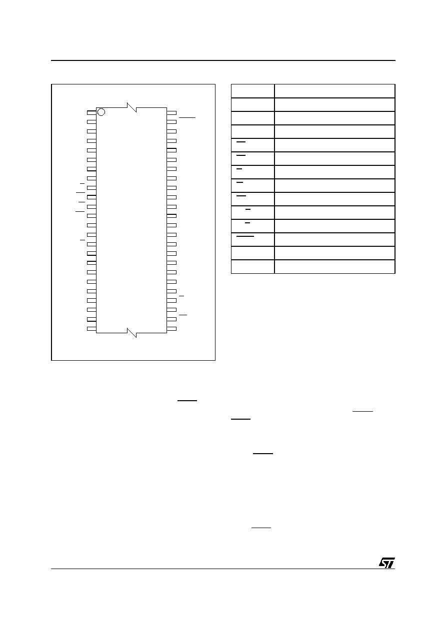
A0-A18
EE
DQ0-DQ14
VCC
M39832
G
EF
VSS
15
W
ERB
RP
FRB
DQ15A≠1
BYTE
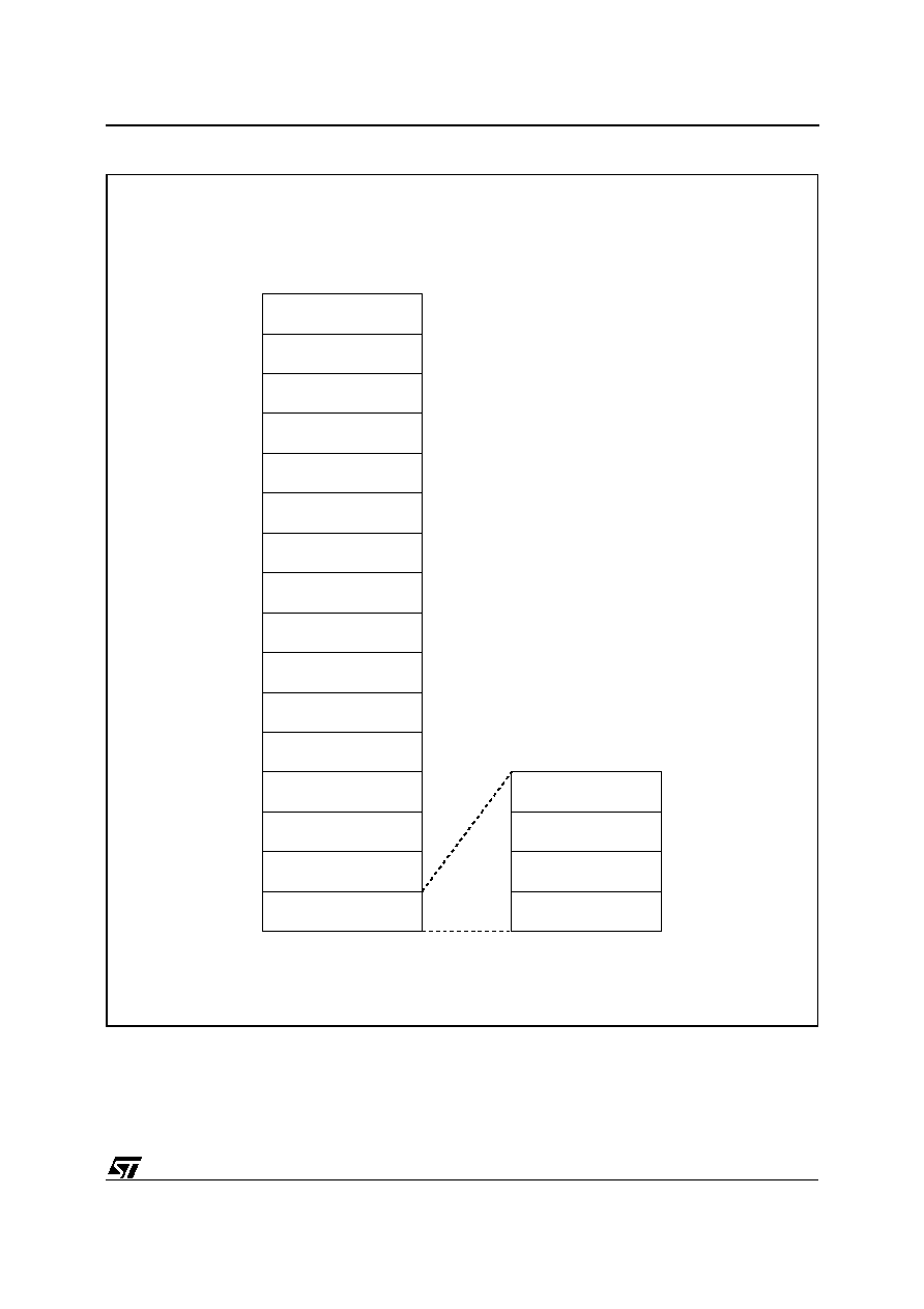
Figure 1. Logic Diagram
M39832
Single Chip 8 Mbit (1Mb x8 or 512Kb x16) Flash and
256 Kbit Parallel EEPROM Memory
PRELIMINARY DATA
2.7V to 3.6V SUPPLY VOLTAGE for
PROGRAM, ERASE and READ OPARATIONS
FLASH ARRAY
≠ Boot block (Top or Bottom location)
≠ Parameter and Main blocks
≠ Selectable x8/x16 Data Bus (BYTE pin).
EEPROM ARRAY
≠ x8 Data Bus only.
120ns ACCESS TIME
(Flash and EEPROM array)
WRITE, PROGRAM and ERASE STATUS BITS
CONCURRENT MODE (Read Flash while
writing to EEPROM)
100,000 ERASE/WRITE CYCLES
10 YEARS DATA RETENTION
LOW POWER CONSUMPTION
≠ Stand-by mode: 100
µ
A
≠ Automatic Stand-by mode
64 bytes ONE TIME PROGRAMMABLE
MEMORY (x8 Data Bus only)
STANDARD EPROM/OTP MEMORY
PACKAGE
EXTENDED TEMPERATURE RANGES
DESCRIPTION
The M39832 is a memory device combining Flash
and EEPROM into a single chip and using single
supply voltage. The memory is mapped in two
arrays: 8 Mbit of Flash memory and 256 Kbit of
EEPROM memory. Each space is independant for
writing, in concurrent mode the Flash Memory can
be read while the EEPROM is being written.
An additional 64 bytes of EPROM are One Time
Programmable.
The M39832 EEPROM memory array is organized
in byte only (regardless on the BYTE pin). It may
be written by byte or by page of 64 bytes and the
integrity of the data can be secured with the help
of the Software Data Protection (SDP).
TSOP48 (NE)
12 x 20 mm
February 1999
1/36
This is preliminary information on a new product now in development or undergoing evaluation. Details are subject to change without notice.
Warning: NC = Not Connected.
VSS
DQ8
DQ1
A6
A1
EF
A3
A2
EE
DQ14
A9
A10
DQ12
W
A15
DQ10
DQ6
VCC
DQ9
DQ2
DQ3
DQ11
DQ4
RP
NC
A18
A7
FRB
NC
A17
AI00845
M39832
12
1
13
24
25
36
37
48
A0
A8
DQ13
ERB
DQ5
A5
DQ0
A4
G
A16
BYTE
VSS
DQ15A≠1
DQ7
A13
A14
A12
A11
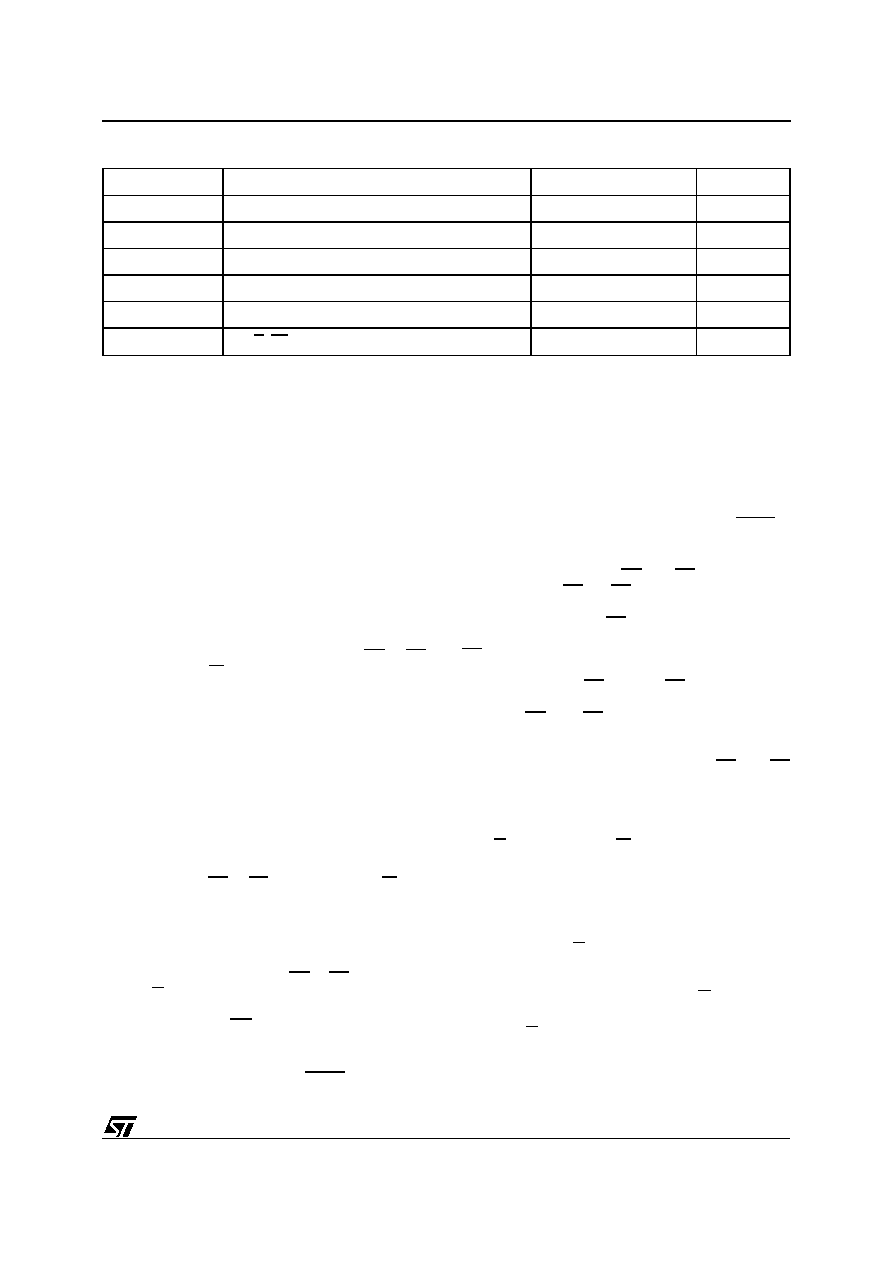
Figure 2. TSOP Pin Connections
A0-A18
Address Inputs
DQ0-DQ7
Data Input/Outputs, Commands Input
DQ8-DQ14
Data Input/Outputs
DQ15A≠1
Data Input/Outputs or Address Input
EE
EEPROM Array Enable
EF
Flash Array Enable
G
Output Enable
W
Write Enable
RP
Reset/Block Temporary Unprotect
ERB
EEPROM Ready/Busy Output
FRB
Flash Ready/Busy Output
BYTE
Flash Array Byte/Word Organization
V
CC
Supply Voltage
V
SS
Ground
Table 1. Signal Names
DESCRIPTION (cont'd)
The M39832 Flash Memory array can be config-
ured as 1Mb x8 or 512Kb x16 with the BYTE input
pin. The M39832-T and M39832-B feature asymet-
rically blocked architecture providing system mem-
ory integration. Both M39832-B and M39832-T
devices have a Flash array of 19 blocks, one Boot
Block of 16 KBytes or 8 KWords, two Parameter
Blocks of 8 KBytes or 4 KWords, one Main Block
of 32 KBytes or 16 KWords and fifteen Main Blocks
of 64 KBytes or 32 KWords. The M39832-T has the
Boot Block at the top of the memory address space
and the M39832-B locates the Boot Block starting
at the bottom. The memory maps are showed in
Figures 3A and 3B. Each block can be erased
separately,any combination of blocks can be speci-
fied for multi-block erase or the entire chip may be
erased. The Erase operations are managed auto-
matically. The block erase operation can be sus-
pended in order to read from or program to any
block not being ersased, and then resumed. Block
protection provides additional data security. Each
block can be separately protected or unprotected
against Program or Erase on programming equip-
ment. All previously protected blocks can be tem-
porarily unprotected in the application. The Flash
memory array is functionally compatible with the
M29W800 Single Voltage Flash Memory device.
During a Program or Erase cycle in the Flash array
or during a Write in the EEPROM array, status bits
available on certain DQn pins provide information
on the M39832 internal logic.
PIN DESCRIPTION
Byte/Word Organization Select (BYTE). The
BYTE input selects the output configuration for the
Flash array: Byte-wide (x8) mode or Word-wide
(x16) mode. The EEPROM array and the 64 Bytes
OTP Row are always accessed Byte-wide (x8).
When BYTE is High, the Word-wide mode is se-
lected for the Flash array (x16) and the data are
read and programmed on DQ0-DQ15. The Flash
array is accessed with A0-A18 Adrress lines. In this
mode, data in the EEPROM array (x8) are read and
programmed on DQ0-DQ7 and the array is ac-
cessed with A0-A14. The 64 bytes OTP are read
and programmed on DQ0-DQ7 and are accessed
with A0-A5 and A6 = 0.
When BYTE is Low, the Byte-wide mode is selected
for the Flash array (x8) and the data are read and
2/36
M39832
programmed on DQ0-DQ7. In this mode, DQ8-
DQ14 are at high impedance and DQ15A≠1 is the
LSB address bit, making the Flash array to be
accessed with A≠1-A18 Adress lines. In this mode,
data in the EEPROM array (x8) are read and
programmed on DQ0-DQ7 and the array is ac-
cessed with A≠1-A13. The 64 bytes OTP are read
and programmed on DQ0-DQ7 and are accessed
with A-1 - A4 and A6 = 0.
Address Inputs (A0-A18). The address inputs for
the memory array are latched during a write opera-
tion on the falling edge at Chip Enable (EE or EF)
or Write Enable W. In Word-wide organisation the
address lines are A0-A18, in Byte-wide organisa-
tion DQ15A≠1 acts as an additional LSB address
line. When A9 is raised to V
ID
, either a Read
Electronic Signature Manufacturer or Device Code,
Block Protection Status or a Write Block Protection
or Block Unprotection is enabled depending on the
combination of levels on A0, A1, A6, A12 and A15.
Data Input/Output (DQ0-DQ7). T he s e I n-
puts/Outputs are used in the Byte-wide and Word-
wide organisations. The input is data to be
programmed in the memory array or a command
to be written. Both are latched on the rising edge
of Chip Enable (EE or EF) or Write Enable W. The
output is data from the Memory Array, the Elec-
tronic Signature Manufacturer or Device codes, the
Block Protection Status or the Status register Data
Polling bit DQ7, the Toggle Bits DQ6 and DQ2, the
Error bit DQ5 or the Erase Timer bit DQ3. Outputs
are valid when Chip Enable (EE or EF) and Output
Enable G are active. The output is high impedance
when the chip is deselected or the outputs are
disabled and when RP is at a Low level.
Data Input/Outputs (DQ8-DQ14 and DQ15A≠1).
These Inputs/Outputs are additionally used in the
Word-wide organisation. When BYTE is High DQ8-
DQ14 and DQ15A≠1 act as the MSB of the Data
Input or Output, functioning as described for DQ0-
DQ7 above, and DQ8 - DQ15 are 'don't care' for
command inputs or status outputs. When BYTE is
Low, DQ8-DQ14 are high impedance, DQ15A≠1 is
the Address A≠1 input.
Memory Array Enable (EE and EF). The Memory
Array Enable (EE or EF) activates the memory
control logic, input buffers, decoders and sense
amplifiers. When the EE input is driven high, the
EEPROM memory array is not selected; when the
EF input is driven high, the Flash memory array is
not selected. Attempts to access both EEPROM
and Flash arrays (EE low and EF low) are forbid-
den. Switching between the two memory array
enables (EE and EF) must not be made on the
same clock cycle, a delay of greater than t
EHFL
must
be inserted.
The M39832 is in standby when both EF and EE
are High (when no internal Erase or programming
is running). The power consumption is reduced to
the standby level and the outputs are in the high
impedance state, independent of the Output En-
able G or Write Enable W inputs.
After 150ns of inactivity and when the addresses
are driven at CMOS levels, the chip automatically
enters a pseudo standby mode where consumption
is reduced to the CMOS standby value, while the
outputs continue to drive the bus.
Output Enable (G). The Output Enable gates the
outputs through the data buffers during a read
operation. The data outputs are in the high imped-
ance state when the Output Enable G is High.
During Block Protect and Block Unprotect opera-
tions, the G input must be forced to V
ID
level (12V
+ 0.5V) (for Flash memory array only).
Symbol
Parameter
Value
Unit
T
A
Ambient Operating Temperature
≠40 to 85
∞
C
T
BIAS
Temperature Under Bias
≠50 to 125
∞
C
T
STG
Storage Temperature
≠65 to 150
∞
C
V
IO
(2)
Input or Output Voltages
≠0.6 to 5
V
V
CC
Supply Voltage
≠0.6 to 5
V
V
A9
, V
G
, V
EF
(2)
A9, G, EF Voltage
≠0.6 to 13.5
V
Notes: 1. Except for the rating "Operating Temperature Range", stresses above those listed in the Table "Absolute Maximum Ratings"
may cause permanent damage to the device. These are stress ratings only and operation of the device at these or any other
conditions above those indicated in the Operating sections of this specification is not implied. Exposure to Absolute Maximum
Rating conditions for extended periods may affect device reliability. Refer also to the STMicroelectronics SURE Program and other
relevant quality documents.
2. Minimum Voltage may undershoot to ≠2V during transition and for less than 20ns.
Table 2. Absolute Maximum Ratings
(1)
3/36
M39832
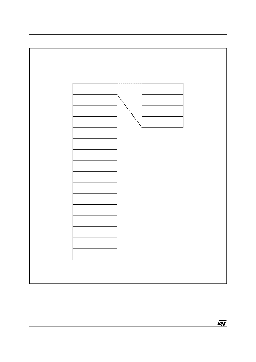
16K BOOT BLOCK
AI01725B
8K PARAMETER BLOCK
8K PARAMETER BLOCK
32K MAIN BLOCK
TOP BOOT BLOCK
FFFFFh
90000h
8FFFFh
80000h
7FFFFh
C0000h
BFFFFh
00000h
64K MAIN BLOCK
64K MAIN BLOCK
64K MAIN BLOCK
64K MAIN BLOCK
64K MAIN BLOCK
64K MAIN BLOCK
B0000h
AFFFFh
A0000h
9FFFFh
60000h
5FFFFh
70000h
6FFFFh
F0000h
EFFFFh
E0000h
DFFFFh
D0000h
CFFFFh
64K MAIN BLOCK
64K MAIN BLOCK
64K MAIN BLOCK
64K MAIN BLOCK
64K MAIN BLOCK
64K MAIN BLOCK
64K MAIN BLOCK
50000h
4FFFFh
30000h
2FFFFh
40000h
3FFFFh
64K MAIN BLOCK
64K MAIN BLOCK
10000h
0FFFFh
20000h
1FFFFh
FFFFFh
F0000h
FC000h
FBFFFh
FA000h
F9FFFh
F8000h
F7FFFh
7FFFFh
48000h
47FFFh
40000h
3FFFFh
60000h
5FFFFh
58000h
57FFFh
50000h
4FFFFh
30000h
2FFFFh
38000h
37FFFh
78000h
77FFFh
70000h
6FFFFh
68000h
67FFFh
Byte-Wide
Word-Wide
7FFFFh
78000h
7E000h
7DFFFh
7D000h
7CFFFh
7C000h
7BFFFh
00000h
28000h
27FFFh
18000h
17FFFh
20000h
1FFFFh
08000h
07FFFh
10000h
0FFFFh
Byte-Wide
Word-Wide
Figure 3A. Top Boot Block Memory Map and Block Address Table
4/36
M39832
16K BOOT BLOCK
AI01731B
8K PARAMETER BLOCK
8K PARAMETER BLOCK
32K MAIN BLOCK
BOTTOM BOOT BLOCK
FFFFFh
90000h
8FFFFh
80000h
7FFFFh
C0000h
BFFFFh
00000h
64K MAIN BLOCK
64K MAIN BLOCK
64K MAIN BLOCK
64K MAIN BLOCK
64K MAIN BLOCK
64K MAIN BLOCK
B0000h
AFFFFh
A0000h
9FFFFh
60000h
5FFFFh
70000h
6FFFFh
F0000h
EFFFFh
E0000h
DFFFFh
D0000h
CFFFFh
64K MAIN BLOCK
64K MAIN BLOCK
64K MAIN BLOCK
64K MAIN BLOCK
64K MAIN BLOCK
64K MAIN BLOCK
64K MAIN BLOCK
50000h
4FFFFh
30000h
2FFFFh
40000h
3FFFFh
64K MAIN BLOCK
64K MAIN BLOCK
10000h
0FFFFh
20000h
1FFFFh
0FFFFh
00000h
08000h
07FFFh
06000h
05FFFh
04000h
03FFFh
FFFFFh
7FFFFh
48000h
47FFFh
40000h
3FFFFh
60000h
5FFFFh
58000h
57FFFh
50000h
4FFFFh
30000h
2FFFFh
38000h
37FFFh
78000h
77FFFh
70000h
6FFFFh
68000h
67FFFh
07FFFh
00000h
04000h
03FFFh
03000h
02FFFh
02000h
01FFFh
00000h
28000h
27FFFh
18000h
17FFFh
20000h
1FFFFh
08000h
07FFFh
10000h
0FFFFh
Byte-Wide
Word-Wide
Byte-Wide
Word-Wide
Figure 3B. Bottom Boot Block Memory Map and Block Address Table
5/36
M39832