1/15
May 2002
M40Z111
M40Z111W
5V OR 3V NVRAM SUPERVISOR FOR UP TO TWO LPSRAMs
FEATURES SUMMARY
s
CONVERT LOW POWER SRAMs INTO
NVRAMs
s
PRECISION POWER MONITORING and
POWER SWITCHING CIRCUITRY
s
AUTOMATIC WRITE-PROTECTION WHEN
V
CC
IS OUT-OF-TOLERANCE
s
CHOICE OF SUPPLY VOLTAGES and
POWER-FAIL DESELECT VOLTAGES:
≠ M40Z111: V
CC
= 4.5 to 5.5V
THS = V
SS
; 4.5
V
PFD
4.75V
THS = V
OUT
; 4.2
V
PFD
4.5V
≠ M40Z111W: V
CC
= 3.0 to 3.6V
THS = V
SS
; 2.8
V
PFD
3.0V
V
CC
= 2.7 to 3.3V
THS = V
OUT
; 2.5
V
PFD
2.7V
s
LESS THAN 15ns CHIP ENABLE ACCESS
PROPAGATION DELAY (for 5.0V device)
s
PACKAGING INCLUDES A 28-LEAD SOIC and
SNAPHAT
Æ
TOP (to be ordered separately)
s
SOIC PACKAGE PROVIDES DIRECT
CONNECTION FOR A SNAPHAT TOP WHICH
CONTAINS THE BATTERY
Figure 1. 28-pin SOIC Package
SOH28 (MH)
SNAPHAT (SH)
Battery
28
1

M40Z111, M40Z111W
2/15
TABLE OF CONTENTS
SUMMARY DESCRIPTION . . . . . . . . . . . . . . . . . . . . . . . . . . . . . . . . . . . . . . . . . . . . . . . . . . . . . . . . . . . 3
Logic Diagram (Figure 2.) . . . . . . . . . . . . . . . . . . . . . . . . . . . . . . . . . . . . . . . . . . . . . . . . . . . . . . . . . 3
Signal Names (Table 1.) . . . . . . . . . . . . . . . . . . . . . . . . . . . . . . . . . . . . . . . . . . . . . . . . . . . . . . . . . . 3
SOIC28 Connections (Figure 3.) . . . . . . . . . . . . . . . . . . . . . . . . . . . . . . . . . . . . . . . . . . . . . . . . . . . . 3
Hardware Hookup (Figure 4.) . . . . . . . . . . . . . . . . . . . . . . . . . . . . . . . . . . . . . . . . . . . . . . . . . . . . . . 4
MAXIMUM RATING. . . . . . . . . . . . . . . . . . . . . . . . . . . . . . . . . . . . . . . . . . . . . . . . . . . . . . . . . . . . . . . . . 4
Absolute Maximum Ratings (Table 2.) . . . . . . . . . . . . . . . . . . . . . . . . . . . . . . . . . . . . . . . . . . . . . . . 4
DC AND AC PARAMETERS. . . . . . . . . . . . . . . . . . . . . . . . . . . . . . . . . . . . . . . . . . . . . . . . . . . . . . . . . . 5
DC and AC Measurement Conditions (Table 3.) . . . . . . . . . . . . . . . . . . . . . . . . . . . . . . . . . . . . . . . . 5
AC Testing Load Circuit (Figure 5.) . . . . . . . . . . . . . . . . . . . . . . . . . . . . . . . . . . . . . . . . . . . . . . . . . . 5
Capacitance (Table 4.) . . . . . . . . . . . . . . . . . . . . . . . . . . . . . . . . . . . . . . . . . . . . . . . . . . . . . . . . . . . 5
DC Characteristics (Table 5.) . . . . . . . . . . . . . . . . . . . . . . . . . . . . . . . . . . . . . . . . . . . . . . . . . . . . . . 6
OPERATION . . . . . . . . . . . . . . . . . . . . . . . . . . . . . . . . . . . . . . . . . . . . . . . . . . . . . . . . . . . . . . . . . . . . . . 7
Data Retention Lifetime Calculation . . . . . . . . . . . . . . . . . . . . . . . . . . . . . . . . . . . . . . . . . . . . . . . . . 7
Power Down Timing (Figure 6.) . . . . . . . . . . . . . . . . . . . . . . . . . . . . . . . . . . . . . . . . . . . . . . . . . . . . . 8
Power Up Timing (Figure 7.) . . . . . . . . . . . . . . . . . . . . . . . . . . . . . . . . . . . . . . . . . . . . . . . . . . . . . . . 8
Power Down/Up AC Characteristics (Table 6.) . . . . . . . . . . . . . . . . . . . . . . . . . . . . . . . . . . . . . . . . . 9
V
CC
Noise And Negative Going Transients . . . . . . . . . . . . . . . . . . . . . . . . . . . . . . . . . . . . . . . . . . . . 9
Supply Voltage Protection (Figure 8.) . . . . . . . . . . . . . . . . . . . . . . . . . . . . . . . . . . . . . . . . . . . . . . . . 9
PART NUMBERING . . . . . . . . . . . . . . . . . . . . . . . . . . . . . . . . . . . . . . . . . . . . . . . . . . . . . . . . . . . . . . . 10
Battery Table (Table 8.) . . . . . . . . . . . . . . . . . . . . . . . . . . . . . . . . . . . . . . . . . . . . . . . . . . . . . . . . . . 10
PACKAGE MECHANICAL INFORMATION . . . . . . . . . . . . . . . . . . . . . . . . . . . . . . . . . . . . . . . . . . . . . 11
REVISION HISTORY. . . . . . . . . . . . . . . . . . . . . . . . . . . . . . . . . . . . . . . . . . . . . . . . . . . . . . . . . . . . . . . 14
3/15
M40Z111, M40Z111W
SUMMARY DESCRIPTION
The M40Z111/W NVRAM SUPERVISOR is a self-
contained device which converts a standard low-
power SRAM into a non-volatile memory.
A precision voltage reference and comparator
monitors the V
CC
input for an out-of-tolerance con-
dition.
When an invalid V
CC
condition occurs, the condi-
tioned chip enable (E
CON
) output is forced inactive
to write-protect the stored data in the SRAM.
During a power failure, the SRAM is switched from
the V
CC
pin to the lithium cell within the
SNAPHAT
Æ
to provide the energy required for
data retention. On a subsequent power-up, the
SRAM remains write protected until a valid power
condition returns.
The 28-pin, 330mil SOIC provides sockets with
gold plated contacts at both ends for direct con-
nection to a separate SNAPHAT housing contain-
ing the battery. The unique design allows the
SNAPHAT battery package to be mounted on top
of the SOIC package after the completion of the
surface mount process.
Insertion of the SNAPHAT housing after reflow
prevents potential battery damage due to the high
temperatures required for device surface-mount-
ing. The SNAPHAT housing is keyed to prevent
reverse insertion.
The SOIC and battery packages are shipped sep-
arately in plastic anti-static tubes or in Tape & Reel
form. For the 28-lead SOIC, the battery package
(e.g.,
SNAPHAT)
part
number
is
"M4Z28-
BR00SH" or "M4Z32-BR00SH" (See Table 8,
page 10).
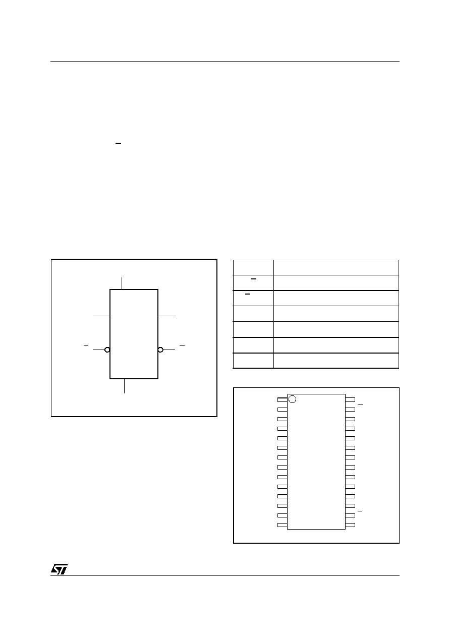
Figure 2. Logic Diagram
Table 1. Signal Names
Figure 3. SOIC28 Connections
AI02238B
THS
VCC
M40Z111
M40Z111W
ECON
VSS
E
VOUT
THS
Threshold Select Input
E
Chip Enable Input
E
CON
Conditioned Chip Enable Output
V
OUT
Supply Voltage Output
V
CC
Supply Voltage
V
SS
Ground
NC
Not Connected Internally
AI02239B
8
2
3
4
5
6
7
9
10
11
12
13
14
22
21
20
19
18
17
16
15
28
27
26
25
24
23
1
NC
NC
NC
NC
VCC
NC
VCC
NC
NC
NC
NC
NC
NC
NC
E
NC
NC
NC
NC
NC
THS
NC
VSS
ECON
NC
NC
VOUT
VCC
M40Z111
M40Z111W

M40Z111, M40Z111W
4/15
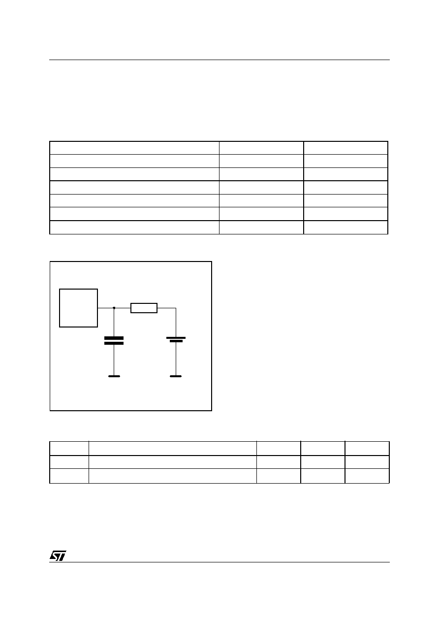
Figure 4. Hardware Hookup
MAXIMUM RATING
Stressing the device above the rating listed in the
"Absolute Maximum Ratings" table may cause
permanent damage to the device. These are
stress ratings only and operation of the device at
these or any other conditions above those indicat-
ed in the Operating sections of this specification is
not implied. Exposure to Absolute Maximum Rat-
ing conditions for extended periods may affect de-
vice
reliability.
Refer
also
to
the
STMicroelectronics SURE Program and other rel-
evant quality documents.
Table 2. Absolute Maximum Ratings
Note: 1. Reflow at peak temperature of 215∞C to 225∞C for < 60 seconds (total thermal budget not to exceed 180∞C for between 90 to 120
seconds).
CAUTION: Negative undershoots below ≠0.3V are not allowed on any pin while in the Battery Back-up mode.
CAUTION: Do NOT wave solder SOIC to avoid damaging SNAPHAT sockets.
AI02394
VCC
E
E2
ECON
VSS
VOUT
VCC
CMOS
SRAM
x8 or x16
3.0, 3.3, or 5V
THS
E
0.1
µ
F
0.1
µ
F
M40Z111/W
Thereshold
1N5817 or
MBR5120T3
Symbol
Parameter
Value
Unit
T
A
Ambient Operating Temperature
Grade 6
≠40 to 85
∞C
T
STG
Storage Temperature (V
CC
Off)
SNAPHAT
Æ
≠40 to 85
∞C
SOIC
≠55 to 125
∞C
T
SLD
(1)
Lead Solder Temperature for 10 seconds
260
∞C
V
IO
Input or Output Voltages
≠0.3 to V
CC
+0.3
V
V
CC
Supply Voltage
M40Z111
≠0.3 to 7.0
V
M40Z111W
≠0.3 to 4.6
V
I
O
Output Current
20
mA
P
D
Power Dissipation
1
W
5/15
M40Z111, M40Z111W
DC AND AC PARAMETERS
This section summarizes the operating and mea-
surement conditions, as well as the DC and AC
characteristics of the device. The parameters in
the following DC and AC Characteristic tables are
derived from tests performed under the Measure-
ment Conditions listed in the relevant tables. De-
signers should check that the operating conditions
in their projects match the measurement condi-
tions when using the quoted parameters.
Table 3. DC and AC Measurement Conditions
Note: Note that Output Hi-Z is defined as the point where data is no longer driven.
Figure 5. AC Testing Load Circuit
Note: 1. 50pF for M40Z111W.
Table 4. Capacitance
Note: 1. Effective capacitance measured with power supply at 5V (M40Z111) or 3.3V (M40Z111W); sampled only, not 100% tested.
2. At 25∞C, f = 1MHz.
3. Outputs deselected
Parameter
M40Z111
M40Z111W
V
CC
Supply Voltage
4.5 to 5.5V
2.7 to 3.6V
Ambient Operating Temperature
≠40 to 85∞C
≠40 to 85∞C
Load Capacitance (C
L
)
100pF
50pF
Input Rise and Fall Times
5ns
5ns
Input Pulse Voltages
0 to 3V
0 to 3V
Input and Output Timing Ref. Voltages
1.5V
1.5V
AI02326
CL = 100pF
(1)
or 5pF
CL includes JIG capacitance
645
DEVICE
UNDER
TEST
1.75V
Symbol
Parameter
(1,2)
Min
Max
Unit
C
IN
Input Capacitance
8
pF
C
OUT
(3)
Output Capacitance
10
pF