1/20
November 2002
M41T00
SERIAL ACCESS TIMEKEEPER
Æ
FEATURES SUMMARY
s
2.0 TO 5.5V CLOCK OPERATING VOLTAGE
s
COUNTERS FOR SECONDS, MINUTES,
HOURS, DAY, DATE, MONTH, YEARS, and
CENTURY
s
YEAR 2000 COMPLIANT
s
SOFTWARE CLOCK CALIBRATION
s
AUTOMATIC SWITCH-OVER and DESELECT
CIRCUITRY
s
I
2
C BUS COMPATIBLE
s
ULTRA-LOW BATTERY SUPPLY CURRENT
OF 1µA
s
LOW OPERATING CURRENT OF 300µA
s
BATTERY OR SUPER-CAP BACK-UP
s
BATTERY BACK-UP NOT RECOMMENDED
FOR 3.0V APPLICATIONS (CAPACITOR
BACK-UP ONLY)
s
OPERATING TEMPERATURE OF ≠40 TO
85∞C
s
AUTOMATIC LEAP YEAR COMPENSATION
s
SPECIAL SOFTWARE PROGRAMMABLE
OUTPUT
Figure 1. 8-pin SOIC Package
8
1
SO8 (M)

M41T00
2/20
TABLE OF CONTENTS
SUMMARY DESCRIPTION . . . . . . . . . . . . . . . . . . . . . . . . . . . . . . . . . . . . . . . . . . . . . . . . . . . . . . . . . . . 3
Logic Diagram (Figure 2.) . . . . . . . . . . . . . . . . . . . . . . . . . . . . . . . . . . . . . . . . . . . . . . . . . . . . . . . . . 3
SOIC Connections (Figure 3.) . . . . . . . . . . . . . . . . . . . . . . . . . . . . . . . . . . . . . . . . . . . . . . . . . . . . . . 3
Signal Names (Table 1.) . . . . . . . . . . . . . . . . . . . . . . . . . . . . . . . . . . . . . . . . . . . . . . . . . . . . . . . . . . 3
Block Diagram (Figure 4.) . . . . . . . . . . . . . . . . . . . . . . . . . . . . . . . . . . . . . . . . . . . . . . . . . . . . . . . . . 4
MAXIMUM RATING. . . . . . . . . . . . . . . . . . . . . . . . . . . . . . . . . . . . . . . . . . . . . . . . . . . . . . . . . . . . . . . . . 5
Absolute Maximum Ratings (Table 2.) . . . . . . . . . . . . . . . . . . . . . . . . . . . . . . . . . . . . . . . . . . . . . . . 5
DC AND AC PARAMETERS. . . . . . . . . . . . . . . . . . . . . . . . . . . . . . . . . . . . . . . . . . . . . . . . . . . . . . . . . . 6
Operating and AC Measurement Conditions (Table 3.) . . . . . . . . . . . . . . . . . . . . . . . . . . . . . . . . . . 6
AC Testing Input/Output Waveform (Figure 5.) . . . . . . . . . . . . . . . . . . . . . . . . . . . . . . . . . . . . . . . . . 6
Capacitance (Table 4.) . . . . . . . . . . . . . . . . . . . . . . . . . . . . . . . . . . . . . . . . . . . . . . . . . . . . . . . . . . . 6
DC Characteristics (Table 5.) . . . . . . . . . . . . . . . . . . . . . . . . . . . . . . . . . . . . . . . . . . . . . . . . . . . . . . 7
Crystal Electrical Characteristics (Table 6.). . . . . . . . . . . . . . . . . . . . . . . . . . . . . . . . . . . . . . . . . . . . 7
OPERATION . . . . . . . . . . . . . . . . . . . . . . . . . . . . . . . . . . . . . . . . . . . . . . . . . . . . . . . . . . . . . . . . . . . . . . 8
2-Wire Bus Characteristics . . . . . . . . . . . . . . . . . . . . . . . . . . . . . . . . . . . . . . . . . . . . . . . . . . . . . . . . 8
Serial Bus Data Transfer Sequence (Figure 6.) . . . . . . . . . . . . . . . . . . . . . . . . . . . . . . . . . . . . . . . . 9
Acknowledgement Sequence (Figure 7.) . . . . . . . . . . . . . . . . . . . . . . . . . . . . . . . . . . . . . . . . . . . . . 9
Bus Timing Requirements Sequence (Figure 8.) . . . . . . . . . . . . . . . . . . . . . . . . . . . . . . . . . . . . . . . 9
AC Characteristics (Table 7.) . . . . . . . . . . . . . . . . . . . . . . . . . . . . . . . . . . . . . . . . . . . . . . . . . . . . . 10
READ Mode. . . . . . . . . . . . . . . . . . . . . . . . . . . . . . . . . . . . . . . . . . . . . . . . . . . . . . . . . . . . . . . . . . . 11
WRITE Mode . . . . . . . . . . . . . . . . . . . . . . . . . . . . . . . . . . . . . . . . . . . . . . . . . . . . . . . . . . . . . . . . . . 11
Slave Address Location (Figure 9.) . . . . . . . . . . . . . . . . . . . . . . . . . . . . . . . . . . . . . . . . . . . . . . . . . 11
READ Mode Sequence (Figure 10.) . . . . . . . . . . . . . . . . . . . . . . . . . . . . . . . . . . . . . . . . . . . . . . . . 12
Alternate READ Mode Sequence (Figure 11.) . . . . . . . . . . . . . . . . . . . . . . . . . . . . . . . . . . . . . . . . 12
WRITE Mode Sequence (Figure 12.) . . . . . . . . . . . . . . . . . . . . . . . . . . . . . . . . . . . . . . . . . . . . . . . 12
Data Retention Mode. . . . . . . . . . . . . . . . . . . . . . . . . . . . . . . . . . . . . . . . . . . . . . . . . . . . . . . . . . . . 13
Power Down/Up Mode AC Waveforms (Figure 13.) . . . . . . . . . . . . . . . . . . . . . . . . . . . . . . . . . . . . 13
Power Down/Up AC Characteristics (Table 8.) . . . . . . . . . . . . . . . . . . . . . . . . . . . . . . . . . . . . . . . . 13
Power Down/Up Trip Points DC Characteristics (Table 9.) . . . . . . . . . . . . . . . . . . . . . . . . . . . . . . . 13
CLOCK OPERATION . . . . . . . . . . . . . . . . . . . . . . . . . . . . . . . . . . . . . . . . . . . . . . . . . . . . . . . . . . . . . . 14
Register Map (Table 10.) . . . . . . . . . . . . . . . . . . . . . . . . . . . . . . . . . . . . . . . . . . . . . . . . . . . . . . . . . 14
Clock Calibration . . . . . . . . . . . . . . . . . . . . . . . . . . . . . . . . . . . . . . . . . . . . . . . . . . . . . . . . . . . . . . . 15
Output Driver Pin . . . . . . . . . . . . . . . . . . . . . . . . . . . . . . . . . . . . . . . . . . . . . . . . . . . . . . . . . . . . . . . 15
Initial Power-on Defaults . . . . . . . . . . . . . . . . . . . . . . . . . . . . . . . . . . . . . . . . . . . . . . . . . . . . . . . . . 15
Crystal Accuracy Across Temperature (Figure 14.) . . . . . . . . . . . . . . . . . . . . . . . . . . . . . . . . . . . . 16
Clock Calibration (Figure 15.) . . . . . . . . . . . . . . . . . . . . . . . . . . . . . . . . . . . . . . . . . . . . . . . . . . . . . 16
PART NUMBERING . . . . . . . . . . . . . . . . . . . . . . . . . . . . . . . . . . . . . . . . . . . . . . . . . . . . . . . . . . . . . . . 17
PACKAGE MECHANICAL INFORMATION . . . . . . . . . . . . . . . . . . . . . . . . . . . . . . . . . . . . . . . . . . . . . 18
REVISION HISTORY. . . . . . . . . . . . . . . . . . . . . . . . . . . . . . . . . . . . . . . . . . . . . . . . . . . . . . . . . . . . . . . 19
3/20
M41T00
SUMMARY DESCRIPTION
The M41T00 TIMEKEEPER
Æ
RAM is a low power
Serial TIMEKEEPER with a built-in 32.768kHz os-
cillator (external crystal controlled). Eight bytes of
the RAM are used for the clock/calendar function
and are configured in binary coded decimal (BCD)
format. Addresses and data are transferred serial-
ly via a two-line bi-directional bus. The built-in ad-
dress register is incremented automatically after
each WRITE or READ data byte.
The M41T00 clock has a built-in power sense cir-
cuit which detects power failures and automatical-
ly switches to the battery supply during power
failures. The energy needed to sustain the RAM
and clock operations can be supplied from a small
lithium coin cell.
Typical data retention time is in excess of 5 years
with a 50mA/h 3V lithium cell (see Data Retention
Mode, page 13 for AC/DC Characteristics). The
M41T00 is supplied in 8 lead Plastic Small Outline
package.
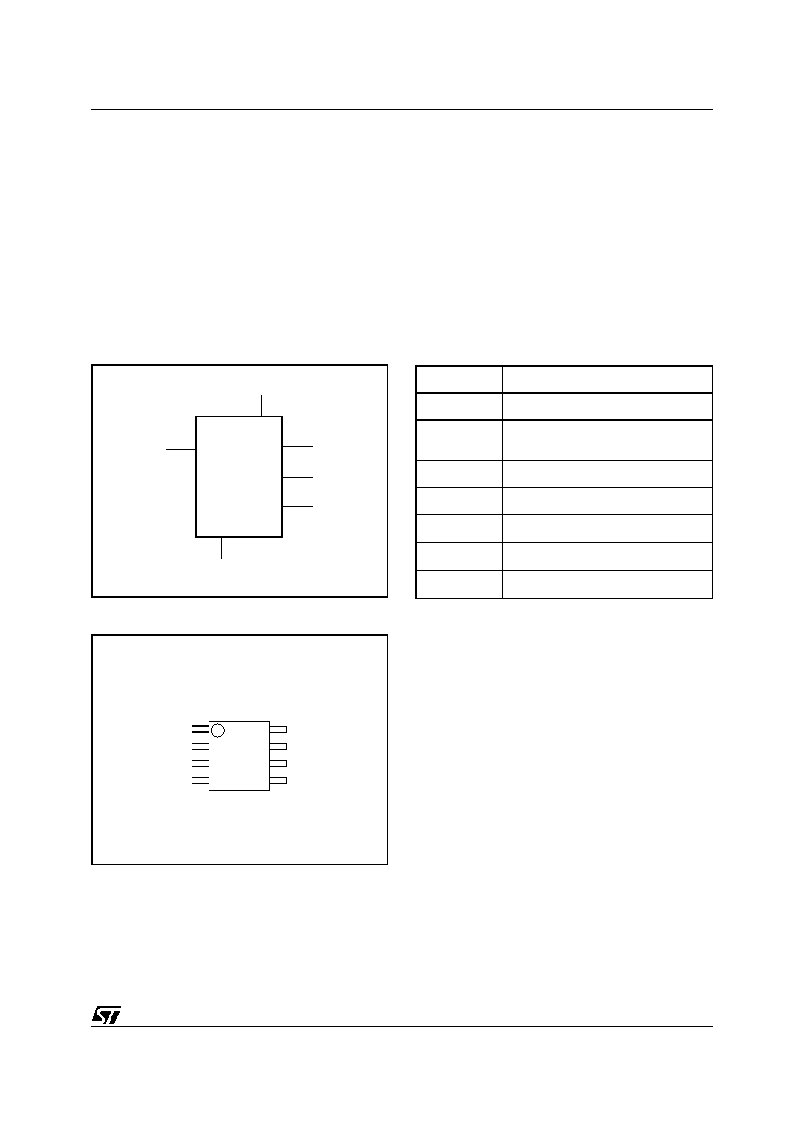
Figure 2. Logic Diagram
Figure 3. SOIC Connections
Table 1. Signal Names
AI00530
OSCI
VCC
M41T00
VSS
SCL
OSCO
SDA
FT/OUT
VBAT
1
SDA
VSS
SCL
FT/OUT
OSCO
OSCI
VCC
VBAT
AI00531
M41T00
2
3
4
8
7
6
5
OSCI
Oscillator Input
OCSO
Oscillator Output
FT/OUT
Frequency Test / Output Driver
(Open Drain)
SDA
Serial Data Address Input / Output
SCL
Serial Clock
V
BAT
Battery Supply Voltage
V
CC
Supply Voltage
V
SS
Ground