1/26
March 2003
Rev. 2.2
M41T256Y
256 Kbit (32K x8) SERIAL RTC
FEATURES SUMMARY
s
5V OPERATING VOLTAGE
s
SERIAL INTERFACE SUPPORTS EXTENDED
I
2
C BUS ADDRESSING (400 KHz)
s
AUTOMATIC SWITCH-OVER and DESELECT
CIRCUITRY
s
POWER-FAIL DESELECT VOLTAGES:
≠ M41T256Y: V
CC
= 4.5 to 5.5V;
V
PFD
= 4.2 < V
PFD
< 4.5V
s
COUNTERS FOR TENTHS/HUNDREDTHS
OF SECONDS, SECONDS, MINUTES,
HOURS, DAY, DATE, MONTH, and YEAR
s
PROGRAMMABLE SOFTWARE CLOCK
CALIBRATION
s
32,752 BYTES OF GENERAL PURPOSE RAM
s
MICROPROCESSOR POWER-ON RESET
s
HOLDS MICROPROCESSOR IN RESET
UNTIL SUPPLY VOLTAGE REACHES
STABLE OPERATING LEVEL
s
AUTOMATIC ADDRESS-INCREMENTING
s
TAMPER INDICATION CIRCUIT with TIME-
STAMP
s
SLEEP MODE FUNCTION
s
PACKAGING INCLUDES A 44-LEAD SOIC and
SNAPHAT
Æ
TOP (to be ordered separately)
s
SOIC PACKAGE PROVIDES DIRECT
CONNECTION FOR A SNAPHAT
Æ
TOP
WHICH CONTAINS THE BATTERY and
CRYSTAL
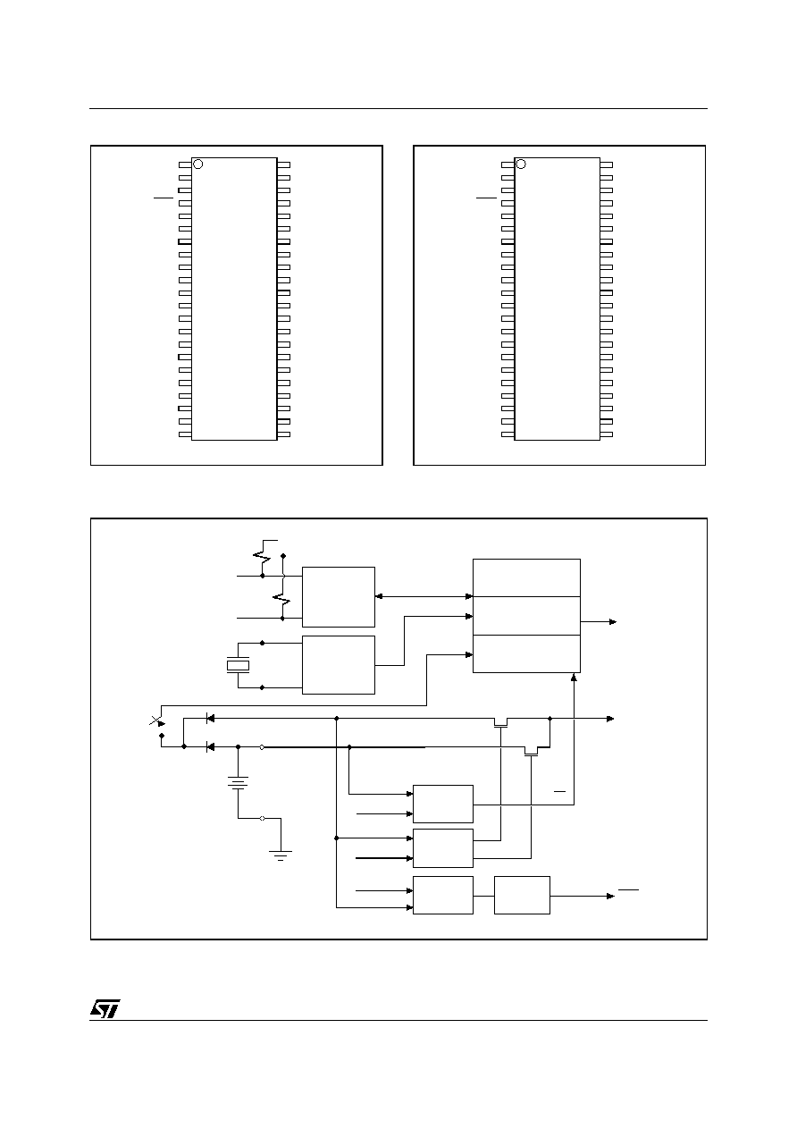
Figure 1. 44-pin, Hatless SOIC Package
Figure 2. 44-pin SOIC Package
44
1
SO44 (MT)
44
1
SOH44 (MH)
SNAPHAT (SH)
Crystal/Battery

M41T256Y
2/26
TABLE OF CONTENTS
SUMMARY DESCRIPTION . . . . . . . . . . . . . . . . . . . . . . . . . . . . . . . . . . . . . . . . . . . . . . . . . . . . . . . . . . . 4
Logic Diagram (Figure 3.) . . . . . . . . . . . . . . . . . . . . . . . . . . . . . . . . . . . . . . . . . . . . . . . . . . . . . . . . . 4
Signal Names (Table 1.) . . . . . . . . . . . . . . . . . . . . . . . . . . . . . . . . . . . . . . . . . . . . . . . . . . . . . . . . . . 4
44-pin SOIC Connections (MT) (Figure 4.) . . . . . . . . . . . . . . . . . . . . . . . . . . . . . . . . . . . . . . . . . . . . 5
Block Diagram (Figure 6.) . . . . . . . . . . . . . . . . . . . . . . . . . . . . . . . . . . . . . . . . . . . . . . . . . . . . . . . . . 5
MAXIMUM RATING. . . . . . . . . . . . . . . . . . . . . . . . . . . . . . . . . . . . . . . . . . . . . . . . . . . . . . . . . . . . . . . . . 6
Absolute Maximum Ratings (Table 2.) . . . . . . . . . . . . . . . . . . . . . . . . . . . . . . . . . . . . . . . . . . . . . . . 6
DC AND AC PARAMETERS. . . . . . . . . . . . . . . . . . . . . . . . . . . . . . . . . . . . . . . . . . . . . . . . . . . . . . . . . . 7
DC and AC Measurement Conditions (Table 3.) . . . . . . . . . . . . . . . . . . . . . . . . . . . . . . . . . . . . . . . . 7
AC Testing Input/Output Waveforms (Figure 7.) . . . . . . . . . . . . . . . . . . . . . . . . . . . . . . . . . . . . . . . . 7
Capacitance (Table 4.) . . . . . . . . . . . . . . . . . . . . . . . . . . . . . . . . . . . . . . . . . . . . . . . . . . . . . . . . . . . 7
DC Characteristics (Table 5.) . . . . . . . . . . . . . . . . . . . . . . . . . . . . . . . . . . . . . . . . . . . . . . . . . . . . . . 8
Crystal Electrical Characteristics (Externally Supplied) (Table 6.). . . . . . . . . . . . . . . . . . . . . . . . . . . 8
OPERATING MODES . . . . . . . . . . . . . . . . . . . . . . . . . . . . . . . . . . . . . . . . . . . . . . . . . . . . . . . . . . . . . . . 9
2-Wire Bus Characteristics . . . . . . . . . . . . . . . . . . . . . . . . . . . . . . . . . . . . . . . . . . . . . . . . . . . . . . . 9
Serial Bus Data Transfer Sequence (Figure 8.) . . . . . . . . . . . . . . . . . . . . . . . . . . . . . . . . . . . . . . . 10
Acknowledgement Sequence (Figure 9.) . . . . . . . . . . . . . . . . . . . . . . . . . . . . . . . . . . . . . . . . . . . . 10
Bus Timing Requirements Sequence (Figure 10.) . . . . . . . . . . . . . . . . . . . . . . . . . . . . . . . . . . . . . 11
AC Characteristics (Table 7.) . . . . . . . . . . . . . . . . . . . . . . . . . . . . . . . . . . . . . . . . . . . . . . . . . . . . . 11
READ Mode . . . . . . . . . . . . . . . . . . . . . . . . . . . . . . . . . . . . . . . . . . . . . . . . . . . . . . . . . . . . . . . . . . 12
WRITE Mode. . . . . . . . . . . . . . . . . . . . . . . . . . . . . . . . . . . . . . . . . . . . . . . . . . . . . . . . . . . . . . . . . . 12
Slave Address Location (Figure 11.) . . . . . . . . . . . . . . . . . . . . . . . . . . . . . . . . . . . . . . . . . . . . . . . . 12
READ Mode Sequence (Figure 12.) . . . . . . . . . . . . . . . . . . . . . . . . . . . . . . . . . . . . . . . . . . . . . . . . 13
Alternate READ Mode Sequence (Figure 13.) . . . . . . . . . . . . . . . . . . . . . . . . . . . . . . . . . . . . . . . . 13
WRITE Mode Sequence (Figure 14.) . . . . . . . . . . . . . . . . . . . . . . . . . . . . . . . . . . . . . . . . . . . . . . . 13
Data Retention Mode . . . . . . . . . . . . . . . . . . . . . . . . . . . . . . . . . . . . . . . . . . . . . . . . . . . . . . . . . . . 14
Sleep Mode. . . . . . . . . . . . . . . . . . . . . . . . . . . . . . . . . . . . . . . . . . . . . . . . . . . . . . . . . . . . . . . . . . . 14
Power Down/Up Mode AC Waveforms (Figure 15.) . . . . . . . . . . . . . . . . . . . . . . . . . . . . . . . . . . . . 15
Power Down/Up AC Characteristics (Table 8.) . . . . . . . . . . . . . . . . . . . . . . . . . . . . . . . . . . . . . . . . 15
CLOCK OPERATION . . . . . . . . . . . . . . . . . . . . . . . . . . . . . . . . . . . . . . . . . . . . . . . . . . . . . . . . . . . . . . 16
Reading the Clock . . . . . . . . . . . . . . . . . . . . . . . . . . . . . . . . . . . . . . . . . . . . . . . . . . . . . . . . . . . . . 16
Setting the Clock . . . . . . . . . . . . . . . . . . . . . . . . . . . . . . . . . . . . . . . . . . . . . . . . . . . . . . . . . . . . . . 16
Stopping and Starting the Oscillator . . . . . . . . . . . . . . . . . . . . . . . . . . . . . . . . . . . . . . . . . . . . . . 16
TIMEKEEPERÆ Register Map (Table 9.) . . . . . . . . . . . . . . . . . . . . . . . . . . . . . . . . . . . . . . . . . . . . 17
Power-on Reset . . . . . . . . . . . . . . . . . . . . . . . . . . . . . . . . . . . . . . . . . . . . . . . . . . . . . . . . . . . . . . . 18

3/26
M41T256Y
Tamper Indication Circuit . . . . . . . . . . . . . . . . . . . . . . . . . . . . . . . . . . . . . . . . . . . . . . . . . . . . . . . 18
Tamper Event Time-Stamp . . . . . . . . . . . . . . . . . . . . . . . . . . . . . . . . . . . . . . . . . . . . . . . . . . . . . . 18
Battery Low Warning. . . . . . . . . . . . . . . . . . . . . . . . . . . . . . . . . . . . . . . . . . . . . . . . . . . . . . . . . . . 19
Preferred Power-on/Battery Attach Defaults . . . . . . . . . . . . . . . . . . . . . . . . . . . . . . . . . . . . . . . 19
Preferred Default Values (Table 10.). . . . . . . . . . . . . . . . . . . . . . . . . . . . . . . . . . . . . . . . . . . . . . . . 19
Crystal Accuracy Across Temperature (Figure 16.) . . . . . . . . . . . . . . . . . . . . . . . . . . . . . . . . . . . . 20
Clock Calibration (Figure 17.) . . . . . . . . . . . . . . . . . . . . . . . . . . . . . . . . . . . . . . . . . . . . . . . . . . . . . 20
PACKAGE MECHANICAL INFORMATION . . . . . . . . . . . . . . . . . . . . . . . . . . . . . . . . . . . . . . . . . . . . . 21
PART NUMBERING . . . . . . . . . . . . . . . . . . . . . . . . . . . . . . . . . . . . . . . . . . . . . . . . . . . . . . . . . . . . . . . 24
SNAPHATÆ Battery Table (Table 15.) . . . . . . . . . . . . . . . . . . . . . . . . . . . . . . . . . . . . . . . . . . . . . . 2 4
REVISION HISTORY. . . . . . . . . . . . . . . . . . . . . . . . . . . . . . . . . . . . . . . . . . . . . . . . . . . . . . . . . . . . . . . 25
M41T256Y
4/26
SUMMARY DESCRIPTION
The M41T256Y Serial TIMEKEEPER
Æ
SRAM is a
low power 256 Kbit static CMOS SRAM organized
as 32K words by 8 bits. A built-in 32.768 kHz os-
cillator (external crystal controlled) and 8 bytes of
the SRAM (see Figure 9, page 17) are used for the
clock/calendar function and are configured in bina-
ry coded decimal (BCD) format.
Addresses and data are transferred serially via a
two line, bi-directional I
2
C interface. The built-in
address register is incremented automatically af-
ter each WRITE or READ data byte.
The M41T256Y has a built-in power sense circuit
which detects power failures and automatically
switches to the battery supply when a power fail-
ure occurs. The energy needed to sustain the
SRAM and clock operations can be supplied by a
lithium button-cell supply when a power failure oc-
curs. Functions available to the user include a
non-volatile, time-of-day clock/calendar, and Pow-
er-on Reset. The eight clock address locations
contain the year, month, date, day, hour, minute,
second, and tenths/hundredths of seconds in 24-
hour BCD format. Corrections for 28, 29 (leap year
- valid until year 2100), 30 and 31 day months are
made automatically. The first clock address loca-
tion (7FF8h) stores the clock software calibration
settings as well as the Write Clock Bit.
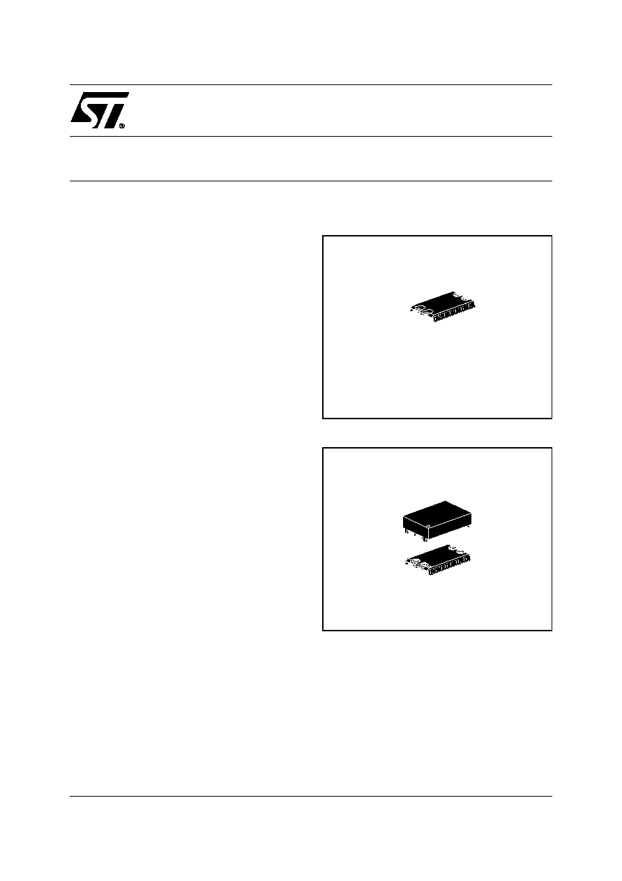
The M41T256Y is supplied in a 44-lead SOIC
SNAPHAT
Æ
package (MH - which integrates both
crystal and battery in a single SNAPHAT top) or a
44-pin "hatless" SOIC (MT). The 44-pin, 330mil
SOIC provides sockets with gold-plated contacts
at both ends for direct connection to a separate
SNAPHAT housing containing the battery and
crystal. The unique design allows the SNAPHAT
battery/crystal package to be mounted on top of
the SOIC package after the completion of the sur-
face-mount process.
Insertion of the SNAPHAT housing after reflow
prevents potential battery and crystal damage due
to the high temperatures required for device sur-
face-mounting. The SNAPHAT housing is also
keyed to prevent reverse insertion. The 44-pin
SOIC and crystal/battery packages are shipped
separately in plastic, anti-static tubes or in Tape &
Reel form. For the 44-lead SOIC, the battery/crys-
tal package (e.g., SNAPHAT) part number is
"M4Txx-BR12SH" (see Table 15, page 24).
Caution: Do not place the SNAPHAT battery/crys-
tal top in conductive foam, as this will drain the lith-
ium, button-cell battery.
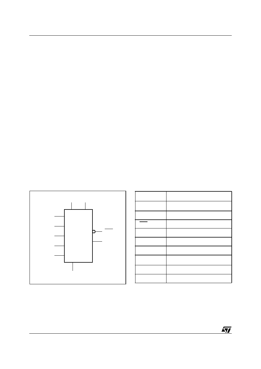
Figure 3. Logic Diagram
Note: 1. For 44-pin SNAPHAT (MT) package only.
Table 1. Signal Names
Note: 1. For 44-pin SNAPHAT (MT) package only.
AI04754b
SCL
VCC
M41T256Y
VSS
SDA
TP
FT
RST
VBAT
(1)
XI
(1)
XO
(1)
XI
(1)
Oscillator Input
XO
(1)
Oscillator Output
FT
Frequency Test (Open drain)
RST
Reset Output (Open drain)
SCL
Serial Clock Input
SDA
Serial Data Input/Output
V
CC
Supply Voltage
V
BAT
(1)
Battery Supply Voltage
V
SS
Ground
TP
Tamper Input