1/20
October 2002
M41T80
SERIAL ACCESS RTC WITH ALARMS
FEATURES SUMMARY
s
2.0 TO 5.5V CLOCK OPERATING VOLTAGE
s
COUNTERS FOR TENTHS/HUNDREDTHS
OF SECONDS, SECONDS, MINUTES,
HOURS, DAY, DATE, MONTH, YEAR, and
CENTURY
s
SERIAL INTERFACE SUPPORTS I
2
C BUS
(400KHz)
s
PROGRAMMABLE ALARM and INTERRUPT
FUNCTION
s
LOW OPERATING CURRENT OF 200µA
s
OPERATING TEMPERATURE OF ≠40 TO
85∞C
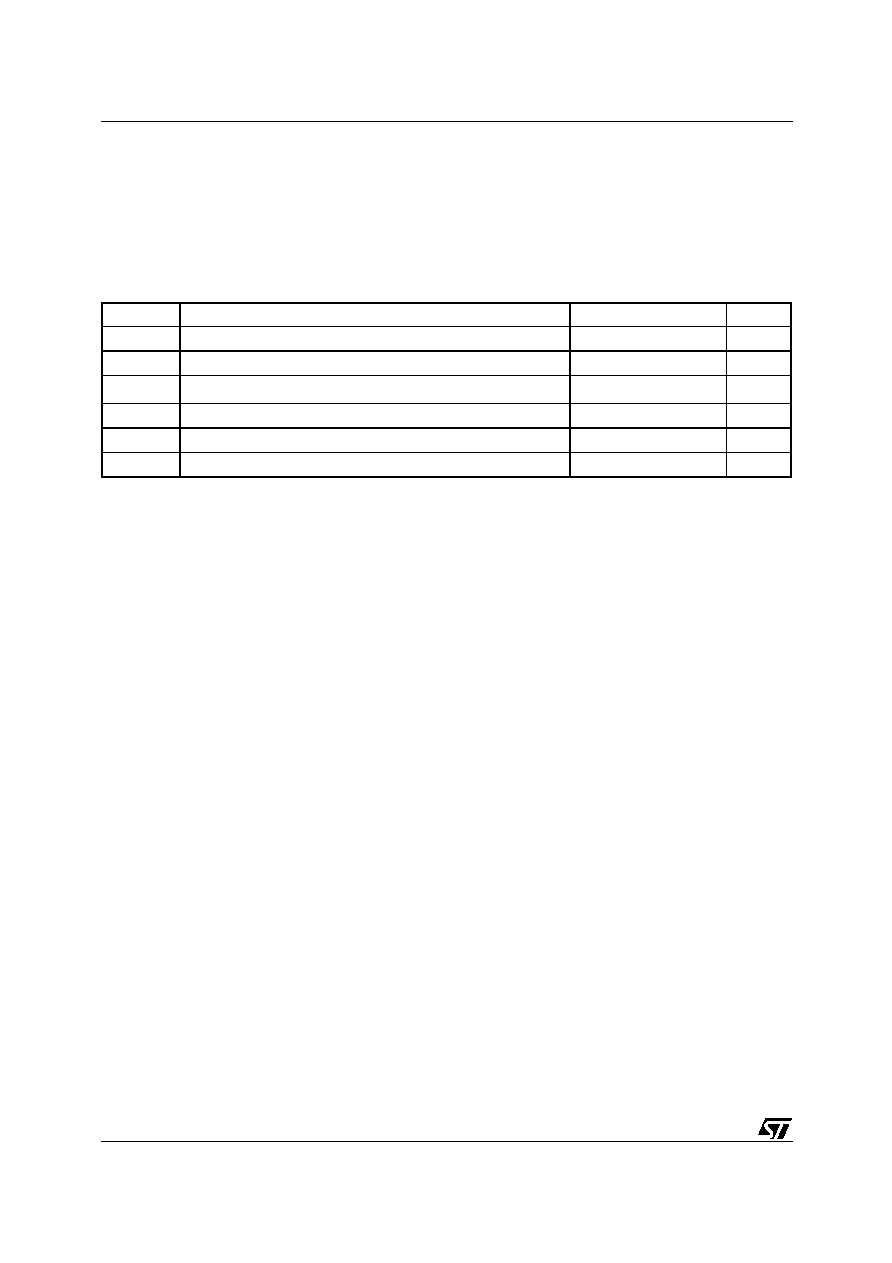
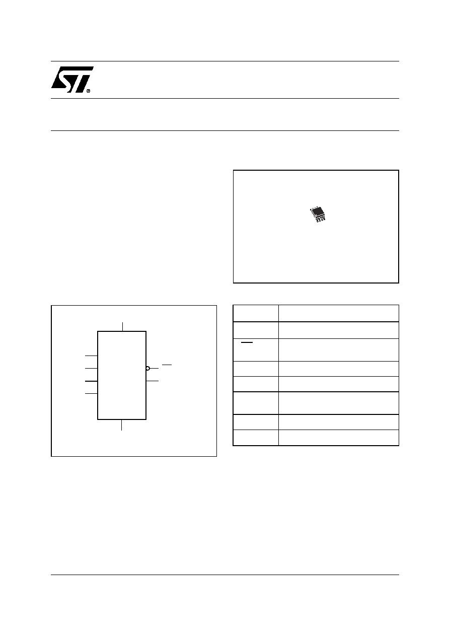
Figure 1. Logic Diagram
Figure 2. 8-pin SOIC Package
Table 1. Signal Names
SCL
VCC
M41T80
VSS
SDA
F32k
IRQ/OUT/SQW
XI
XO
AI07005
XI
Oscillator Input
XO
Oscillator Output
IRQ/OUT/
SQW
Interrupt / Output Driver / Square
Wave (Open Drain)
SDA
Serial Data Input/Output
SCL
Serial Clock Input
F
32k
32kHz Square Wave Output (Open
drain)
V
CC
Supply Voltage
V
SS
Ground
8
1
SO8 (M)

M41T80
2/20
TABLE OF CONTENTS
SUMMARY DESCRIPTION . . . . . . . . . . . . . . . . . . . . . . . . . . . . . . . . . . . . . . . . . . . . . . . . . . . . . . . . . . . 3
8-pin SOIC Connections (Figure 3.) . . . . . . . . . . . . . . . . . . . . . . . . . . . . . . . . . . . . . . . . . . . . . . . . . 3
Block Diagram (Figure 4.) . . . . . . . . . . . . . . . . . . . . . . . . . . . . . . . . . . . . . . . . . . . . . . . . . . . . . . . . . 3
MAXIMUM RATING. . . . . . . . . . . . . . . . . . . . . . . . . . . . . . . . . . . . . . . . . . . . . . . . . . . . . . . . . . . . . . . . . 4
Absolute Maximum Ratings (Table 2.) . . . . . . . . . . . . . . . . . . . . . . . . . . . . . . . . . . . . . . . . . . . . . . . 4
DC AND AC PARAMETERS. . . . . . . . . . . . . . . . . . . . . . . . . . . . . . . . . . . . . . . . . . . . . . . . . . . . . . . . . . 5
Operating and AC Measurement Conditions (Table 3.) . . . . . . . . . . . . . . . . . . . . . . . . . . . . . . . . . . 5
AC Measurement I/O Waveform (Figure 5.) . . . . . . . . . . . . . . . . . . . . . . . . . . . . . . . . . . . . . . . . . . . 5
Capacitance (Table 4.) . . . . . . . . . . . . . . . . . . . . . . . . . . . . . . . . . . . . . . . . . . . . . . . . . . . . . . . . . . . 5
DC Characteristics (Table 5.) . . . . . . . . . . . . . . . . . . . . . . . . . . . . . . . . . . . . . . . . . . . . . . . . . . . . . . 6
Crystal Electrical Characteristics (Table 6.). . . . . . . . . . . . . . . . . . . . . . . . . . . . . . . . . . . . . . . . . . . . 6
OPERATION . . . . . . . . . . . . . . . . . . . . . . . . . . . . . . . . . . . . . . . . . . . . . . . . . . . . . . . . . . . . . . . . . . . . . . 7
2-Wire Bus Characteristics . . . . . . . . . . . . . . . . . . . . . . . . . . . . . . . . . . . . . . . . . . . . . . . . . . . . . . . . 7
Serial Bus Data Transfer Sequence (Figure 6.) . . . . . . . . . . . . . . . . . . . . . . . . . . . . . . . . . . . . . . . . 8
Acknowledgement Sequence (Figure 7.) . . . . . . . . . . . . . . . . . . . . . . . . . . . . . . . . . . . . . . . . . . . . . 8
Bus Timing Requirements Sequence (Figure 8.) . . . . . . . . . . . . . . . . . . . . . . . . . . . . . . . . . . . . . . . 9
AC Characteristics (Table 7.) . . . . . . . . . . . . . . . . . . . . . . . . . . . . . . . . . . . . . . . . . . . . . . . . . . . . . . 9
READ Mode. . . . . . . . . . . . . . . . . . . . . . . . . . . . . . . . . . . . . . . . . . . . . . . . . . . . . . . . . . . . . . . . . . . 10
Slave Address Location (Figure 9.) . . . . . . . . . . . . . . . . . . . . . . . . . . . . . . . . . . . . . . . . . . . . . . . . . 10
READ Mode Sequence (Figure 10.) . . . . . . . . . . . . . . . . . . . . . . . . . . . . . . . . . . . . . . . . . . . . . . . . 10
Alternative READ Mode Sequence (Figure 11.) . . . . . . . . . . . . . . . . . . . . . . . . . . . . . . . . . . . . . . . 11
WRITE Mode . . . . . . . . . . . . . . . . . . . . . . . . . . . . . . . . . . . . . . . . . . . . . . . . . . . . . . . . . . . . . . . . . . 11
WRITE Mode Sequence (Figure 12.) . . . . . . . . . . . . . . . . . . . . . . . . . . . . . . . . . . . . . . . . . . . . . . . 11
CLOCK OPERATION . . . . . . . . . . . . . . . . . . . . . . . . . . . . . . . . . . . . . . . . . . . . . . . . . . . . . . . . . . . . . . 12
TIMEKEEPERÆ Registers. . . . . . . . . . . . . . . . . . . . . . . . . . . . . . . . . . . . . . . . . . . . . . . . . . . . . . . . 12
TIMEKEEPERÆ Register Map (Table 8.) . . . . . . . . . . . . . . . . . . . . . . . . . . . . . . . . . . . . . . . . . . . . 13
Full-time 32kHz Square Wave Output . . . . . . . . . . . . . . . . . . . . . . . . . . . . . . . . . . . . . . . . . . . . . . . 15
Century Bit. . . . . . . . . . . . . . . . . . . . . . . . . . . . . . . . . . . . . . . . . . . . . . . . . . . . . . . . . . . . . . . . . . . . 16
Alarm Interrupt Reset Waveform (Figure 13.) . . . . . . . . . . . . . . . . . . . . . . . . . . . . . . . . . . . . . . . . . 14
Alarm Repeat Modes (Table 9.) . . . . . . . . . . . . . . . . . . . . . . . . . . . . . . . . . . . . . . . . . . . . . . . . . . . 14
Square Wave Output Frequency (Table 10.). . . . . . . . . . . . . . . . . . . . . . . . . . . . . . . . . . . . . . . . . . 15
Century Bit. . . . . . . . . . . . . . . . . . . . . . . . . . . . . . . . . . . . . . . . . . . . . . . . . . . . . . . . . . . . . . . . . . . . 16
Output Driver Pin . . . . . . . . . . . . . . . . . . . . . . . . . . . . . . . . . . . . . . . . . . . . . . . . . . . . . . . . . . . . . . . 16
Preferred Power-on Default. . . . . . . . . . . . . . . . . . . . . . . . . . . . . . . . . . . . . . . . . . . . . . . . . . . . . . . 16
Preferred Power-on Default Values (Table 11.) . . . . . . . . . . . . . . . . . . . . . . . . . . . . . . . . . . . . . . . 16
PART NUMBERING . . . . . . . . . . . . . . . . . . . . . . . . . . . . . . . . . . . . . . . . . . . . . . . . . . . . . . . . . . . . . . . 17
PACKAGE MECHANICAL INFORMATION . . . . . . . . . . . . . . . . . . . . . . . . . . . . . . . . . . . . . . . . . . . . . 18
REVISION HISTORY. . . . . . . . . . . . . . . . . . . . . . . . . . . . . . . . . . . . . . . . . . . . . . . . . . . . . . . . . . . . . . . 19
3/20
M41T80
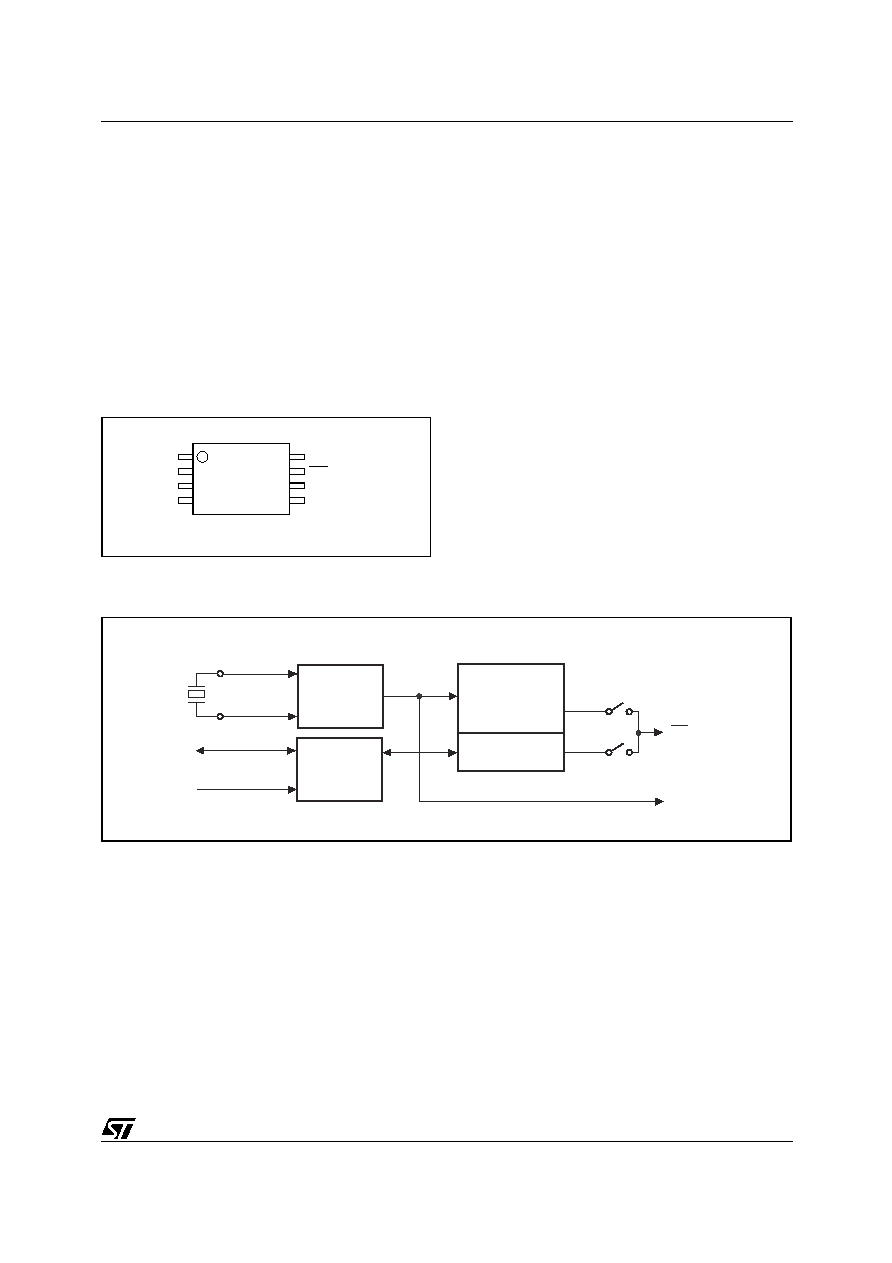
SUMMARY DESCRIPTION
The M41T80 Serial Access TIMEKEEPER
Æ
SRAM is a low power Serial RTC with a built-in
32.768 KHz oscillator (external crystal controlled).
Eight registers (see Table 8, page 13) are used for
the clock/calendar function and are configured in
binary coded decimal (BCD) format. An additional
12 registers provide status/control of Alarm, 32kHz
output, and Square Wave functions. Addresses
and data are transferred serially via a two line, bi-
directional I
2
C interface. The built-in address reg-
ister is incremented automatically after each
WRITE or READ data byte.
Functions available to the user include a time-of-
day clock/calendar, Alarm interrupts, 32kHz out-
put, and programmable Square Wave output. The
eight clock address locations contain the century,
year, month, date, day, hour, minute, second and
tenths/hundredths of a second in 24 hour BCD for-
mat. Corrections for 28, 29 (leap year - valid until
year 2100), 30 and 31 day months are made auto-
matically.
The M41T80 is supplied in an 8-pin SOIC.
Figure 3. 8-pin SOIC Connections
Note: 1. Open drain output.
Figure 4. Block Diagram
Note: 1. Open Drain output
2
3
4
5
6
8
7
1
IRQ/OUT/SQW(1)
SDA
SCL
VSS
XO
F32k
(1)
XI
VCC
M41T80
AI07006
REAL TIME CLOCK
CALENDAR
RTC W/ALARM
SQUARE WAVE
IRQ/OUT/SQW(1)
F32k(1)
AF
SDA
SCL
I2C
INTERFACE
32KHz
OSCILLATOR
CRYSTAL
AI07007
5/20
M41T80
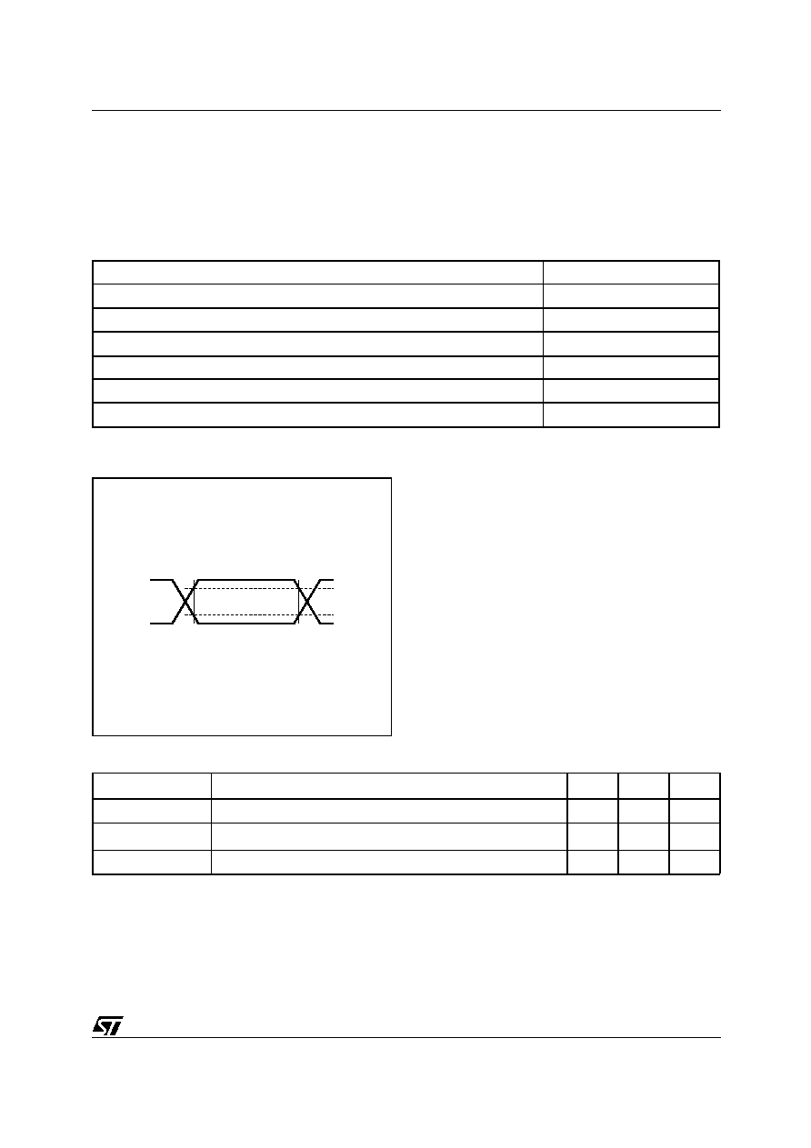
DC AND AC PARAMETERS
This section summarizes the operating and mea-
surement conditions, as well as the DC and AC
characteristics of the device. The parameters in
the following DC and AC Characteristic tables are
derived from tests performed under the Measure-
ment Conditions listed in the relevant tables. De-
signers should check that the operating conditions
in their projects match the measurement condi-
tions when using the quoted parameters.
Table 3. Operating and AC Measurement Conditions
Note: Output Hi-Z is defined as the point where data is no longer driven.
Figure 5. AC Measurement I/O Waveform
Table 4. Capacitance
Note: 1. Effective capacitance measured with power supply at 5V; sampled only, not 100% tested.
2. At 25∞C, f = 1MHz.
3. Outputs deselected.
Parameter
M41T80
Supply Voltage (V
CC
)
2.0 to 5.5V
Ambient Operating Temperature (T
A
)
≠40 to 85∞C
Load Capacitance (C
L
)
100pF
Input Rise and Fall Times
50ns
Input Pulse Voltages
0.2V
CC
to 0.8 V
CC
Input and Output Timing Ref. Voltages
0.3V
CC
to 0.7 V
CC
AI02568
0.8VCC
0.2VCC
0.7VCC
0.3VCC
Symbol
Parameter
(1,2)
Min
Max
Unit
C
IN
Input Capacitance
7
pF
C
OUT
(3)
Output Capacitance
10
pF
t
LP
Low-pass filter input time constant (SDA and SCL)
50
ns