 | –≠–ª–µ–∫—Ç—Ä–æ–Ω–Ω—ã–π –∫–æ–º–ø–æ–Ω–µ–Ω—Ç: M41TM6 | –°–∫–∞—á–∞—Ç—å:  PDF PDF  ZIP ZIP |
1/15
May 2000
M41T00
Serial Access TIMEKEEPER
Æ
s
2.0V to 5.5V SUPPLY VOLTAGE
s
COUNTERS for SECONDS, MINUTES,
HOURS, DAY, DATE, MONTH, YEARS and
CENTURY
s
YEAR 2000 COMPLIANT
s
SOFTWARE CLOCK CALIBRATION
s
AUTOMATIC SWITCH-OVER and DESELECT
CIRCUITRY
s
I
2
C BUS COMPATIBLE
s
ULTRA-LOW BATTERY SUPPLY CURRENT
of 1µA
s
LOW OPERATING CURRENT of 300µA
s
OPERATING TEMPERATURE of ≠40 to 85∞C
s
AUTOMATIC LEAP YEAR COMPENSATION
s
SPECIAL SOFTWARE PROGRAMMABLE
OUTPUT
DESCRIPTION
The M41T00 TIMEKEEPER
Æ
RAM is a low power
Serial TIMEKEEPER with a built-in 32.768kHz os-
cillator (external crystal controlled). Eight bytes of
the RAM are used for the clock/calendar function
and are configured in binary coded decimal (BCD)
format. Addresses and data are transferred serial-
ly via a two-line bi-directional bus. The built-in ad-
dress register is incremented automatically after
each write or read data byte.
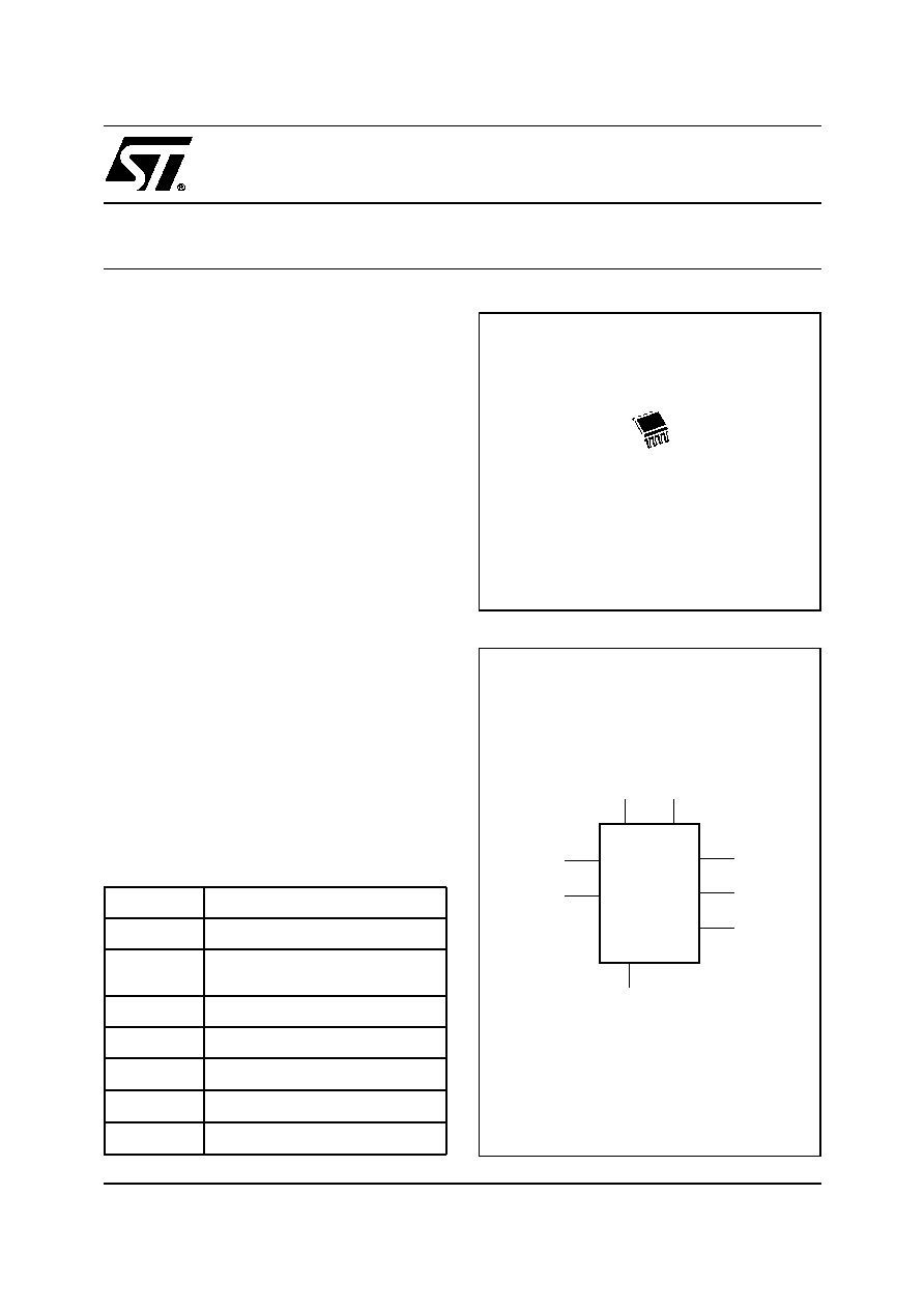
Figure 1. Logic Diagram
AI00530
OSCI
VCC
M41T00
VSS
SCL
OSCO
SDA
FT/OUT
VBAT
8
1
SO8 (M)
150mil Width
Table 1. Signal Names
OSCI
Oscillator Input
OCSO
Oscillator Output
FT/OUT
Frequency Test / Output Driver
(Open Drain)
SDA
Serial Data Address Input / Output
SCL
Serial Clock
V
BAT
Battery Supply Voltage
V
CC
Supply Voltage
V
SS
Ground
M41T00
2/15
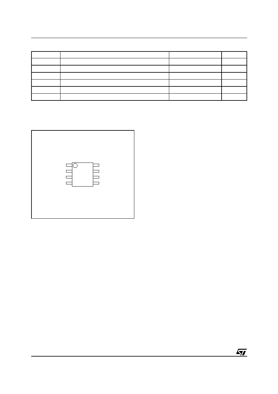
Figure 2. SOIC Connections
1
SDA
VSS
SCL
FT/OUT
OSCO
OSCI
VCC
VBAT
AI00531
M41T00
2
3
4
8
7
6
5
Table 2. Absolute Maximum Ratings
Note: Stresses greater than those listed under "Absolute Maximum Ratings" may cause permanent damage to the device. This is a stress
rating only and functional operation of the device at these or any other conditions above those indicated in the operational section of
this specification is not implied. Exposure to the absolute maximum rating conditions for extended periods of time may affect reliability.
CAUTION: Negative undershoots below ≠0.3V are not allowed on any pin while in the Battery Back-up mode.
Symbol
Parameter
Value
Unit
T
A
Ambient Operating Temperature
≠40 to 85
∞C
T
STG
Storage Temperature (V
CC
Off, Oscillator Off)
≠55 to 125
∞C
V
IO
Input or Output Voltages
≠0.3 to 7
V
V
CC
Supply Voltage
≠0.3 to 7
V
I
O
Output Current
20
mA
P
D
Power Dissipation
0.25
W
The M41T00 clock has a built-in power sense cir-
cuit which detects power failures and automatical-
ly switches to the battery supply during power
failures. The energy needed to sustain the RAM
and clock operations can be supplied from a small
lithium coin cell.
Typical data retention time is in excess of 5years
with a 50mA/h 3V lithium cell. The M41T00 is sup-
plied in 8 lead Plastic Small Outline package.
OPERATION
The M41T00 clock operates as a slave device on
the serial bus. Access is obtained by implementing
a start condition followed by the correct slave ad-
dress (D0h). The 8 bytes contained in the device
can then be accessed sequentially in the following
order:
1.
Seconds Register
2.
Minutes Register
3.
Century/Hours Register
4.
Day Register
5.
Date Register
6.
Month Register
7.
Years Register
8.
Control Register
The M41T00 clock continually monitors V
CC
for an
out of tolerance condition. Should V
CC
fall below
V
SO
, the device terminates an access in progress
and resets the device address counter. Inputs to
the device will not be recognized at this time to
prevent erroneous data from being written to the
device from an out of tolerance system. When V
CC
falls below V
SO
, the device automatically switches
over to the battery and powers down into an ultra
low current mode of operation to conserve battery
life. Upon power-up, the device switches from bat-
tery to V
CC
at V
SO
and recognizes inputs.
3/15
M41T00
Table 3. Register Map
Note: 1. When CEB is set to '1', CB will toggle from '0' to '1' or from '1' to '0' at the turn of the century (dependent upon the initial value set).
When CEB is set to '0', CB will not toggle.
Address
Data
Function/Range
BCD Format
D7
D6
D5
D4
D3
D2
D1
D0
0
ST
10 Seconds
Seconds
Seconds
00-59
1
X
10 Minutes
Minutes
Minutes
00-59
2
CEB
(1)
CB
10 Hours
Hours
Century/Hour
0-1/00-23
3
X
X
X
X
X
Day
Day
01-07
4
X
X
10 Date
Date
Date
01-31
5
X
X
X
10 M.
Month
Month
01-12
6
10 Years
Years
Year
00-99
7
OUT
FT
S
Calibration
Control
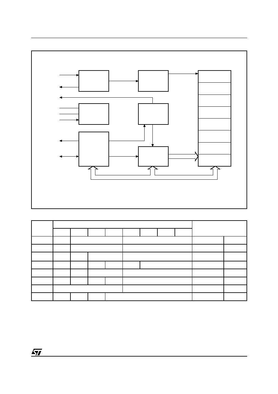
Figure 3. Block Diagram
AI00603
SECONDS
OSCILLATOR
32.768 kHz
VOLTAGE
SENSE and
SWITCH
CIRCUITRY
SERIAL
BUS
INTERFACE
DIVIDER
CONTROL
LOGIC
ADDRESS
REGISTER
MINUTES
CENTURY/HOURS
DAY
DATE
MONTH
YEAR
CONTROL
OSCI
OSCO
FT/OUT
VCC
VSS
VBAT
SCL
SDA
1 Hz
Keys:
S = SIGN Bit
FT = FREQUENCY TEST Bit
ST = STOP Bit
OUT = Output level
X = Don't care
CEB = Century Enable Bit
CB = Century Bit
M41T00
4/15
Table 5. Capacitance
(1, 2)
(T
A
= 25 ∞C, f = 1 MHz)
Note: 1. Effective capacitance measured with power supply at 5V.
2. Sampled only, not 100% tested.
3. Outputs deselected.
Symbol
Parameter
Min
Max
Unit
C
IN
Input Capacitance (SCL)
7
pF
C
OUT
(3)
Output Capacitance (SDA, FT/OUT)
10
pF
t
LP
Low-pass filter input time constant (SDA and SCL)
250
1000
ns
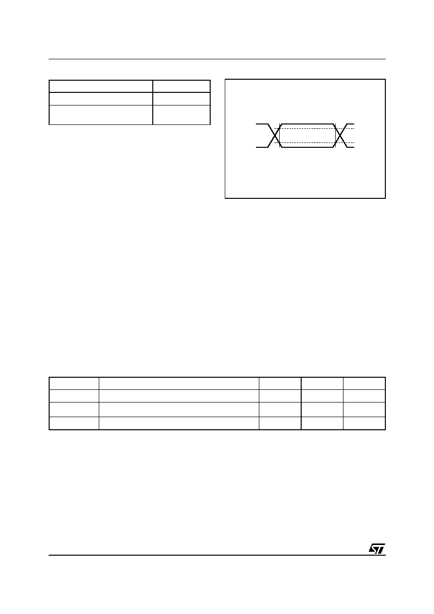
Figure 4. AC Testing Load Circuit
AI02568
0.8VCC
0.2VCC
0.7VCC
0.3VCC
Table 4. AC Measurement Conditions
Note that Output Hi-Z is defined as the point where data is no longer
driven.
Input Rise and Fall Times
5ns
Input Pulse Voltages
0.2V
CC
to 0.8V
CC
Input and Output Timing Ref.
Voltages
0.3V
CC
to 0.7V
CC
2-WIRE BUS CHARACTERISTICS
This bus is intended for communication between
different ICs. It consists of two lines: one bi-direc-
tional for data signals (SDA) and one for clock sig-
nals (SCL). Both the SDA and the SCL lines must
be connected to a positive supply voltage via a
pull-up resistor.
The following protocol has been defined:
≠ Data transfer may be initiated only when the bus
is not busy.
≠ During data transfer, the data line must remain
stable whenever the clock line is High. Changes
in the data line while the clock line is High will be
interpreted as control signals.
Accordingly, the following bus conditions have
been defined:
Bus not busy. Both data and clock lines remain
High.
Start data transfer. A change in the state of the
data line, from High to Low, while the clock is High,
defines the START condition.
Stop data transfer. A change in the state of the
data line, from Low to High, while the clock is High,
defines the STOP condition.
Data valid. The state of the data line represents
valid data when after a start condition, the data line
is stable for the duration of the High period of the
clock signal. The data on the line may be changed
during the Low period of the clock signal. There is
one clock pulse per bit of data.
Each data transfer is initiated with a start condition
and terminated with a stop condition. The number
of data bytes transferred between the start and
stop conditions is not limited. The information is
transmitted byte-wide and each receiver acknowl-
edges with a ninth bit.
By definition, a device that gives out a message is
called "transmitter", the receiving device that gets
the message is called "receiver". The device that
controls the message is called "master". The de-
vices that are controlled by the master are called
"slaves".
5/15
M41T00
Table 6. DC Characteristics
(T
A
= ≠40 to 85∞C; V
CC
= 2.0V to 5.5V)
Note: 1. STMicroelectronics recommends the RAYOVAC BR1225 or BR1632 (or equivalent) as the battery supply.
Table 7. Power Down/Up Trip Points DC Characteristics
(1)
(T
A
= ≠40 to 85∞C)
Note: 1. All voltages referenced to V
SS
.
2. Switch-over and deselect point.
Table 8. Crystal Electrical Characteristics
(Externally Supplied)
Note: Load capacitors are integrated within the M41T00. Circuit board layout considerations for the 32.768kHz crystal of minimum trace
lengths and isolation from RF generating signals should be taken into account.
STMicroelectronics recommends the KDS DT-38 Tuning Fork Type quartz crystal for industrial temperature operations.
KDS can be contacted at 913-491-6825 or http://www.kdsj.co.jp for further information on this crystal type.
Symbol
Parameter
Test Condition
Min
Typ
Max
Unit
I
LI
Input Leakage Current
0V
V
IN
V
CC
±1
µA
I
LO
Output Leakage Current
0V
V
OUT
V
CC
±1
µA
I
CC1
Supply Current
Switch Frequency = 100kHz
300
µA
I
CC2
Supply Current (Standby)
SCL, SDA = V
CC
≠ 0.3V
70
µA
V
IL
Input Low Voltage
≠0.3
0.3 V
CC
V
V
IH
Input High Voltage
0.7 V
CC
V
CC
+ 0.8
V
V
OL
Output Low Voltage
I
OL
= 3mA
0.4
V
V
BAT
(1)
Battery Supply Voltage
2
3
3.5
V
I
BAT
Battery Supply Current
T
A
= 25∞C, V
CC
= 0V,
Oscillator ON, V
BAT
= 3V
0.8
1
µA
Symbol
Parameter
Min
Typ
Max
Unit
V
SO
(2)
Battery Back-up Switchover Voltage
V
BAT
≠ 0.70
V
BAT
≠ 0.50
V
BAT
≠ 0.30
V
Symbol
Parameter
Min
Typ
Max
Unit
f
O
Resonant Frequency
32.768
kHz
R
S
Series Resistance
35
k
C
L
Load Capacitance
12.5
pF