M440T1MV
2/26
TABLE OF CONTENTS
FEATURES SUMMARY . . . . . . . . . . . . . . . . . . . . . . . . . . . . . . . . . . . . . . . . . . . . . . . . . . . . . . . . . . . . . 1
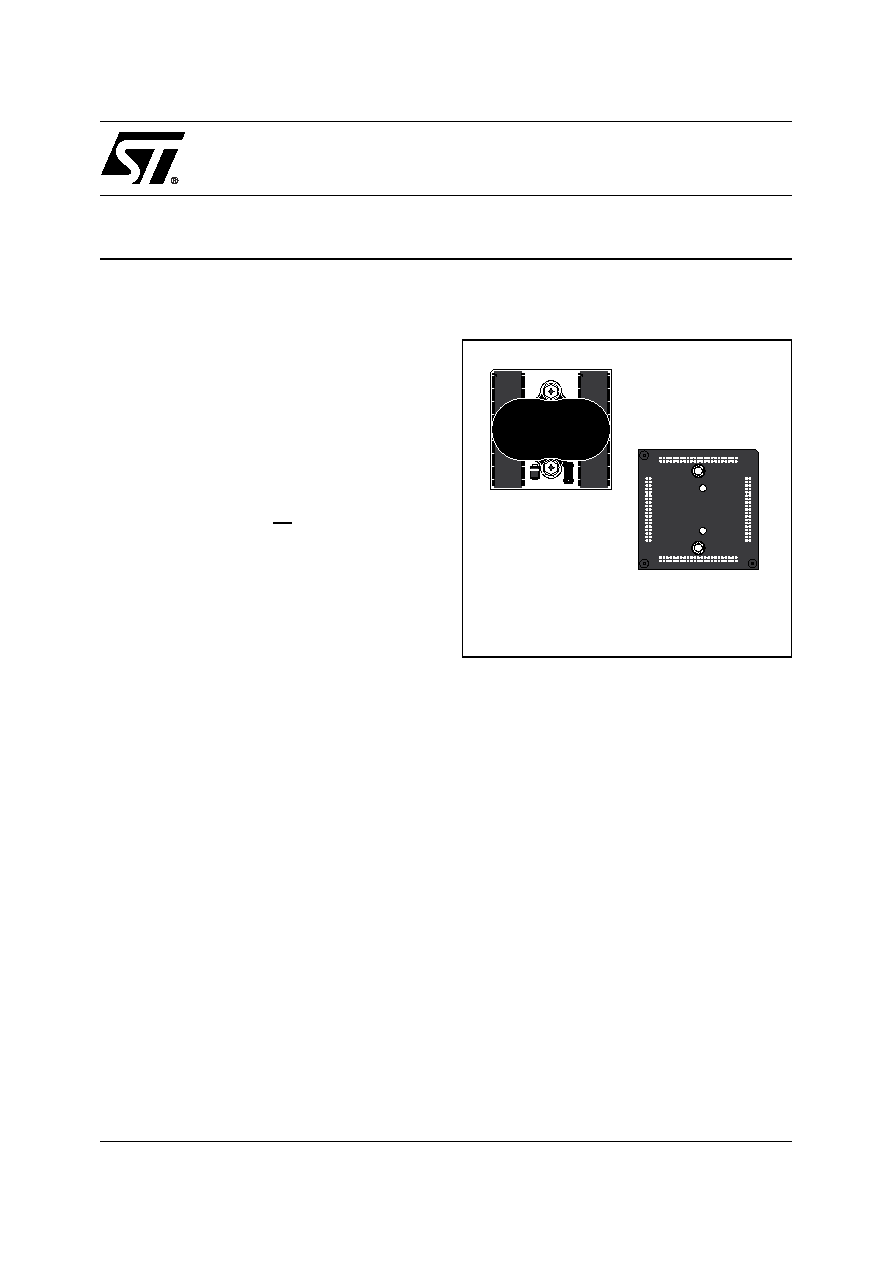
Figure 1. Package. . . . . . . . . . . . . . . . . . . . . . . . . . . . . . . . . . . . . . . . . . . . . . . . . . . . . . . . . . . . . . . 1
SUMMARY DESCRIPTION . . . . . . . . . . . . . . . . . . . . . . . . . . . . . . . . . . . . . . . . . . . . . . . . . . . . . . . . . . . 4
Figure 2. Logic Diagram . . . . . . . . . . . . . . . . . . . . . . . . . . . . . . . . . . . . . . . . . . . . . . . . . . . . . . . . . . 4
Table 1. Signal Names . . . . . . . . . . . . . . . . . . . . . . . . . . . . . . . . . . . . . . . . . . . . . . . . . . . . . . . . . . 4
Figure 3. PBGA Connections (Top View) . . . . . . . . . . . . . . . . . . . . . . . . . . . . . . . . . . . . . . . . . . . . . 5
Figure 4. M440T1MV Hardware Hookup . . . . . . . . . . . . . . . . . . . . . . . . . . . . . . . . . . . . . . . . . . . . . 6
Figure 5. M440T1MV PBGA Module Solution (Side/Top). . . . . . . . . . . . . . . . . . . . . . . . . . . . . . . . . 7
OPERATION MODES . . . . . . . . . . . . . . . . . . . . . . . . . . . . . . . . . . . . . . . . . . . . . . . . . . . . . . . . . . . . . . . 8
Memory READ Mode . . . . . . . . . . . . . . . . . . . . . . . . . . . . . . . . . . . . . . . . . . . . . . . . . . . . . . . . . . . . 8
Clock READ Mode . . . . . . . . . . . . . . . . . . . . . . . . . . . . . . . . . . . . . . . . . . . . . . . . . . . . . . . . . . . . . . 8
Table 2. Memory Operating Modes . . . . . . . . . . . . . . . . . . . . . . . . . . . . . . . . . . . . . . . . . . . . . . . . . 8
Table 3. Clock Operating Modes . . . . . . . . . . . . . . . . . . . . . . . . . . . . . . . . . . . . . . . . . . . . . . . . . . . 9
Figure 6. Memory READ Mode AC Waveforms, Chip Enable- or Output Enable-Controlled . . . . . . 9
Figure 7. Memory READ Mode AC Waveforms, Address-Controlled . . . . . . . . . . . . . . . . . . . . . . . . 9
Figure 8. Clock READ Mode AC Waveforms, Chip Enable- or Output Enable-Controlled . . . . . . . 10
Figure 9. Clock READ Mode AC Waveforms, Address-Controlled. . . . . . . . . . . . . . . . . . . . . . . . . 10
Table 4. Memory/Clock READ Mode AC Characteristics . . . . . . . . . . . . . . . . . . . . . . . . . . . . . . . 10
Memory WRITE Mode . . . . . . . . . . . . . . . . . . . . . . . . . . . . . . . . . . . . . . . . . . . . . . . . . . . . . . . . . . 11
Clock WRITE Mode . . . . . . . . . . . . . . . . . . . . . . . . . . . . . . . . . . . . . . . . . . . . . . . . . . . . . . . . . . . . 11
Figure 10.Memory WRITE Mode AC Waveforms, WRITE Enable-Controlled . . . . . . . . . . . . . . . . 11
Figure 11.Memory WRITE Mode AC Waveforms, Chip Enable-Controlled . . . . . . . . . . . . . . . . . . 12
Figure 12.Clock WRITE Mode AC Waveforms, WRITE Enable-Controlled . . . . . . . . . . . . . . . . . . 12
Figure 13.Clock WRITE Mode AC Waveforms, Chip Enable-Controlled. . . . . . . . . . . . . . . . . . . . . 13
Table 5. Memory/Clock WRITE Mode AC Characteristics . . . . . . . . . . . . . . . . . . . . . . . . . . . . . . 13
CLOCK OPERATION . . . . . . . . . . . . . . . . . . . . . . . . . . . . . . . . . . . . . . . . . . . . . . . . . . . . . . . . . . . . . . 14
Clock Registers . . . . . . . . . . . . . . . . . . . . . . . . . . . . . . . . . . . . . . . . . . . . . . . . . . . . . . . . . . . . . . . 14
Reading and Setting the Clock. . . . . . . . . . . . . . . . . . . . . . . . . . . . . . . . . . . . . . . . . . . . . . . . . . . 14
Clock Alarm Registers . . . . . . . . . . . . . . . . . . . . . . . . . . . . . . . . . . . . . . . . . . . . . . . . . . . . . . . . . 14
Watchdog Alarm Registers. . . . . . . . . . . . . . . . . . . . . . . . . . . . . . . . . . . . . . . . . . . . . . . . . . . . . . 14
Table 6. Register Map . . . . . . . . . . . . . . . . . . . . . . . . . . . . . . . . . . . . . . . . . . . . . . . . . . . . . . . . . . 15
Table 7. Time of Day Alarm Mask Bits . . . . . . . . . . . . . . . . . . . . . . . . . . . . . . . . . . . . . . . . . . . . . 15
Command Register . . . . . . . . . . . . . . . . . . . . . . . . . . . . . . . . . . . . . . . . . . . . . . . . . . . . . . . . . . . . 16
Battery Low . . . . . . . . . . . . . . . . . . . . . . . . . . . . . . . . . . . . . . . . . . . . . . . . . . . . . . . . . . . . . . . . . . 16
Sleep Mode. . . . . . . . . . . . . . . . . . . . . . . . . . . . . . . . . . . . . . . . . . . . . . . . . . . . . . . . . . . . . . . . . . . 16
MAXIMUM RATINGS . . . . . . . . . . . . . . . . . . . . . . . . . . . . . . . . . . . . . . . . . . . . . . . . . . . . . . . . . . . . . . 17
Table 8. Absolute Maximum Ratings . . . . . . . . . . . . . . . . . . . . . . . . . . . . . . . . . . . . . . . . . . . . . . . 17
DC AND AC PARAMETERS. . . . . . . . . . . . . . . . . . . . . . . . . . . . . . . . . . . . . . . . . . . . . . . . . . . . . . . . . 18

3/26
M440T1MV
Table 9. DC and AC Measurement Conditions . . . . . . . . . . . . . . . . . . . . . . . . . . . . . . . . . . . . . . . 18
Figure 14.AC Testing Load Circuit . . . . . . . . . . . . . . . . . . . . . . . . . . . . . . . . . . . . . . . . . . . . . . . . . 18
Table 10. Capacitance. . . . . . . . . . . . . . . . . . . . . . . . . . . . . . . . . . . . . . . . . . . . . . . . . . . . . . . . . . . 18
Table 11. DC Characteristics. . . . . . . . . . . . . . . . . . . . . . . . . . . . . . . . . . . . . . . . . . . . . . . . . . . . . . 19
Data Retention Mode . . . . . . . . . . . . . . . . . . . . . . . . . . . . . . . . . . . . . . . . . . . . . . . . . . . . . . . . . . . 20
Figure 15.Power Down/Up Mode AC Waveforms . . . . . . . . . . . . . . . . . . . . . . . . . . . . . . . . . . . . . . 20
Table 12. Power Down/Up Trip Points DC Characteristics . . . . . . . . . . . . . . . . . . . . . . . . . . . . . . . 20
Table 13. Power Down/Up AC Characteristics . . . . . . . . . . . . . . . . . . . . . . . . . . . . . . . . . . . . . . . . 21
PACKAGE MECHANICAL INFORMATION . . . . . . . . . . . . . . . . . . . . . . . . . . . . . . . . . . . . . . . . . . . . . 22
Figure 16.PBGA-ZA ≠ 168-ball Plastic Ball Grid Array Package Outline . . . . . . . . . . . . . . . . . . . . 22
Table 14. PBGA-ZA ≠ 168-ball Plastic Ball Grid Array Package Mechanical Data . . . . . . . . . . . . . 23
PART NUMBERING . . . . . . . . . . . . . . . . . . . . . . . . . . . . . . . . . . . . . . . . . . . . . . . . . . . . . . . . . . . . . . . 24
Table 15. Ordering Information Scheme . . . . . . . . . . . . . . . . . . . . . . . . . . . . . . . . . . . . . . . . . . . . . 24
REVISION HISTORY. . . . . . . . . . . . . . . . . . . . . . . . . . . . . . . . . . . . . . . . . . . . . . . . . . . . . . . . . . . . . . . 25
Table 16. Document Revision History . . . . . . . . . . . . . . . . . . . . . . . . . . . . . . . . . . . . . . . . . . . . . . . 25

M440T1MV
4/26
SUMMARY DESCRIPTION
The M440T1MV TIMEKEEPER
Æ
RAM is a 16Mbit,
non-volatile static RAM organized as 1,024K by 32
bits and real time clock organized as 64 bytes by
8 bits. The special PBGA package provides a fully
integrated battery back-up memory and real time
clock solution. In the event of power instability or
absence, a self-contained battery maintains the
timekeeping operation and provides power for a
CMOS static RAM. Control circuitry monitors V
CC
and invokes write protection to prevent data cor-
ruption in the memory and RTC.
The clock keeps track of tenths/hundredths of sec-
onds, seconds, minutes, hours, day, date, month,
and year information. The last day of the month is
automatically adjusted for months with less than
31 days, including leap year correction.
The clock operates in one of two formats:
≠
a 12-hour mode with an AM/PM indicator; or
≠
a 24-hour mode
The M440T1MV is in a 168-ball PBGA module that
integrates the RTC, the battery, and SRAM in one
package.
Figure 2. Logic Diagram
Table 1. Signal Names
AI04200
VCC
M440T1MV
VSS
BL
IRQ
RSV2
RSV1
A0 ≠ A19
DQ0 ≠ DQ31
DQC0 ≠ DQC7
EC
W1 ≠ W4
WC
G
GC
E1 ≠ E4
A0 - A19
Address Inputs
DQ0 - DQ31
NVRAM Data Input/Output
DQC0 - DQC7
Clock Data Input/Output
E1 - E4
NVRAM Chip Enable Inputs
EC
Clock Chip Enable Input
W1 - W4
NVRAM WRITE Enable Inputs
WC
Clock WRITE Enable Input
G
Output Enable Input
GC
Clock Output Enable Input
BL
Battery Low Output (Open
Drain)
IRQ
Interrupt Output (Open Drain)
RSV1
Reserved
RSV2
Reserved
NC
No Connect
V
CC
Supply Voltage
V
SS
Ground