1/19
March 2003
Rev. 3.0
M48T02
M48T12
5.0V, 16 Kbit (2Kb x 8) TIMEKEEPER
Æ
SRAM
FEATURES SUMMARY
s
INTEGRATED, ULTRA LOW POWER SRAM,
REAL TIME CLOCK, and POWER-FAIL
CONTROL CIRCUIT
s
BYTEWIDETM RAM-LIKE CLOCK ACCESS
s
BCD CODED YEAR, MONTH, DAY, DATE,
HOURS, MINUTES, and SECONDS
s
TYPICAL CLOCK ACCURACY OF ±1 MINUTE
A MONTH, AT 25∞C
s
SOFTWARE CONTROLLED CLOCK
CALIBRATION FOR HIGH ACCURACY
APPLICATIONS
s
AUTOMATIC POWER-FAIL CHIP DESELECT
and WRITE PROTECTION
s
WRITE PROTECT VOLTAGES
(V
PFD
= Power-fail Deselect Voltage):
≠ M48T02: V
CC
= 4.75 to 5.5V
4.5V
V
PFD
4.75V
≠ M48T12: V
CC
= 4.5 to 5.5V
4.2V
V
PFD
4.5V
s
SELF-CONTAINED BATTERY and CRYSTAL
IN THE CAPHATTM DIP PACKAGE
s
PIN and FUNCTION COMPATIBLE WITH
JEDEC STANDARD 2K x 8 SRAMs
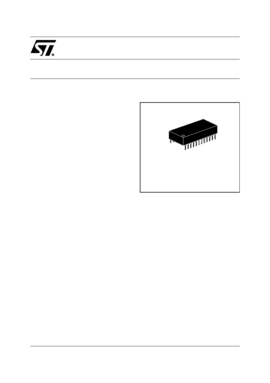
Figure 1. 24-pin PCDIP, CAPHATTM Package
24
1
PCDIP24 (PC)
Battery/Crystal
CAPHAT

M48T02, M48T12
2/19
TABLE OF CONTENTS
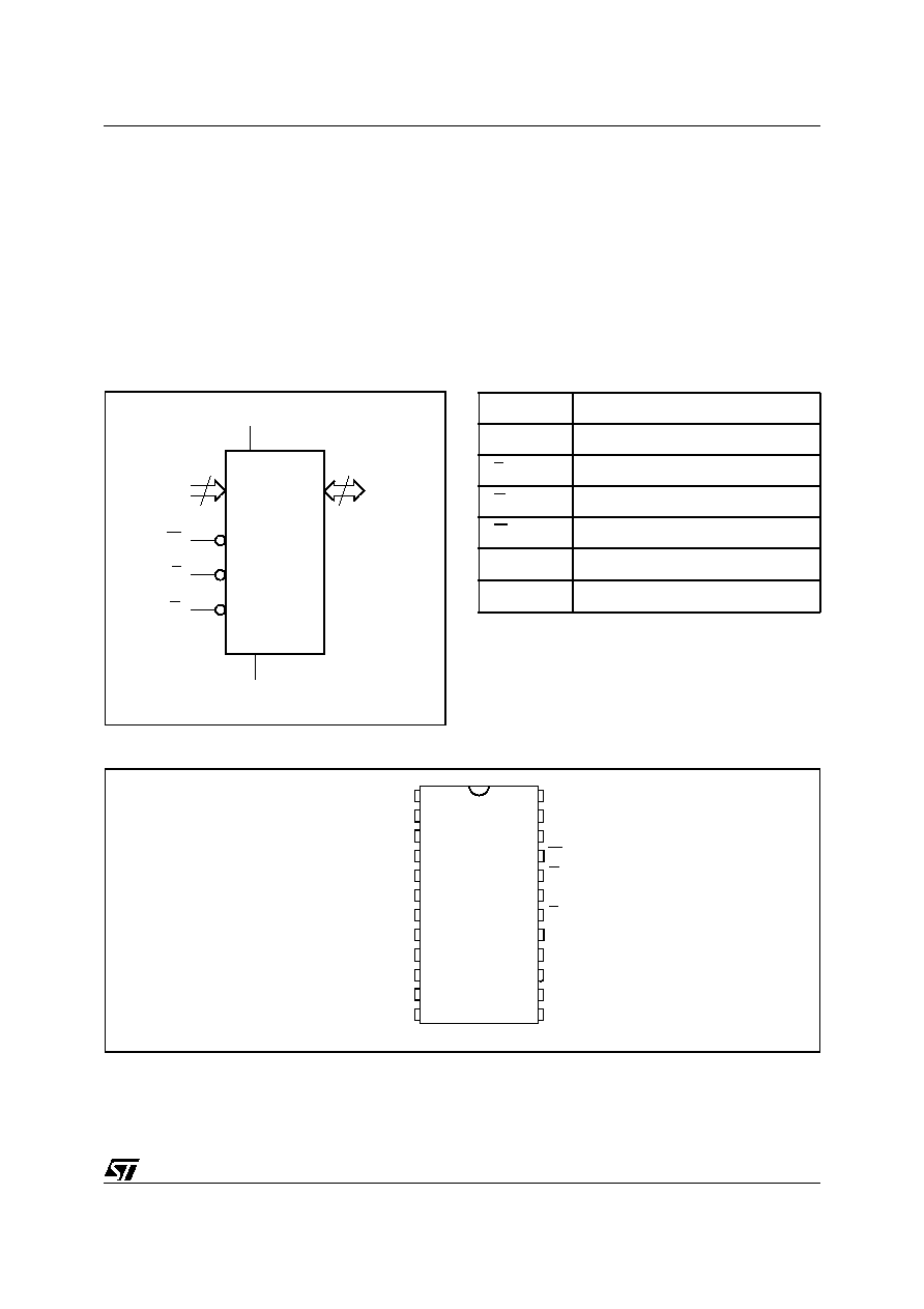
SUMMARY DESCRIPTION . . . . . . . . . . . . . . . . . . . . . . . . . . . . . . . . . . . . . . . . . . . . . . . . . . . . . . . . . . . 3
Figure 2. Logic Diagram . . . . . . . . . . . . . . . . . . . . . . . . . . . . . . . . . . . . . . . . . . . . . . . . . . . . . . . . . . 3
Table 1. Signal Names . . . . . . . . . . . . . . . . . . . . . . . . . . . . . . . . . . . . . . . . . . . . . . . . . . . . . . . . . . . 3
Figure 3. DIP Connections . . . . . . . . . . . . . . . . . . . . . . . . . . . . . . . . . . . . . . . . . . . . . . . . . . . . . . . . 3
Figure 4. Block Diagram . . . . . . . . . . . . . . . . . . . . . . . . . . . . . . . . . . . . . . . . . . . . . . . . . . . . . . . . . . 4
MAXIMUM RATING. . . . . . . . . . . . . . . . . . . . . . . . . . . . . . . . . . . . . . . . . . . . . . . . . . . . . . . . . . . . . . . . . 4
Table 2. Absolute Maximum Ratings . . . . . . . . . . . . . . . . . . . . . . . . . . . . . . . . . . . . . . . . . . . . . . . . . 4
DC AND AC PARAMETERS. . . . . . . . . . . . . . . . . . . . . . . . . . . . . . . . . . . . . . . . . . . . . . . . . . . . . . . . . . 5
Table 3. Operating and AC Measurement Conditions . . . . . . . . . . . . . . . . . . . . . . . . . . . . . . . . . . . . 5
Figure 5. AC Testing Load Circuit . . . . . . . . . . . . . . . . . . . . . . . . . . . . . . . . . . . . . . . . . . . . . . . . . . . 5
Table 4. Capacitance. . . . . . . . . . . . . . . . . . . . . . . . . . . . . . . . . . . . . . . . . . . . . . . . . . . . . . . . . . . . . 5
Table 5. DC Characteristics. . . . . . . . . . . . . . . . . . . . . . . . . . . . . . . . . . . . . . . . . . . . . . . . . . . . . . . . 6
OPERATION MODES . . . . . . . . . . . . . . . . . . . . . . . . . . . . . . . . . . . . . . . . . . . . . . . . . . . . . . . . . . . . . . . 6
Table 6. Operating Modes . . . . . . . . . . . . . . . . . . . . . . . . . . . . . . . . . . . . . . . . . . . . . . . . . . . . . . . . . 6
READ Mode . . . . . . . . . . . . . . . . . . . . . . . . . . . . . . . . . . . . . . . . . . . . . . . . . . . . . . . . . . . . . . . . . . . 7
Figure 6. READ Mode AC Waveforms . . . . . . . . . . . . . . . . . . . . . . . . . . . . . . . . . . . . . . . . . . . . . . . 7
Table 7. READ Mode AC Characteristics . . . . . . . . . . . . . . . . . . . . . . . . . . . . . . . . . . . . . . . . . . . . . 7
WRITE Mode. . . . . . . . . . . . . . . . . . . . . . . . . . . . . . . . . . . . . . . . . . . . . . . . . . . . . . . . . . . . . . . . . . . 8
Figure 7. WRITE Enable Controlled, WRITE AC Waveform . . . . . . . . . . . . . . . . . . . . . . . . . . . . . . . 8
Figure 8. Chip Enable Controlled, WRITE AC Waveforms . . . . . . . . . . . . . . . . . . . . . . . . . . . . . . . . 8
Table 8. WRITE Mode AC Characteristics . . . . . . . . . . . . . . . . . . . . . . . . . . . . . . . . . . . . . . . . . . . . 9
Data Retention Mode . . . . . . . . . . . . . . . . . . . . . . . . . . . . . . . . . . . . . . . . . . . . . . . . . . . . . . . . . . . 10
Figure 9. Checking the BOK Flag Status. . . . . . . . . . . . . . . . . . . . . . . . . . . . . . . . . . . . . . . . . . . . . 10
Figure 10. Power Down/Up Mode AC Waveforms . . . . . . . . . . . . . . . . . . . . . . . . . . . . . . . . . . . . . 11
Table 9. Power Down/Up AC Characteristics . . . . . . . . . . . . . . . . . . . . . . . . . . . . . . . . . . . . . . . . . 11
Table 10. Power Down/Up Trip Points DC Characteristics . . . . . . . . . . . . . . . . . . . . . . . . . . . . . . . 11
CLOCK OPERATIONS . . . . . . . . . . . . . . . . . . . . . . . . . . . . . . . . . . . . . . . . . . . . . . . . . . . . . . . . . . . . . 12
Reading the Clock . . . . . . . . . . . . . . . . . . . . . . . . . . . . . . . . . . . . . . . . . . . . . . . . . . . . . . . . . . . . . 12
Setting the Clock . . . . . . . . . . . . . . . . . . . . . . . . . . . . . . . . . . . . . . . . . . . . . . . . . . . . . . . . . . . . . . 12
Table 11. Register Map . . . . . . . . . . . . . . . . . . . . . . . . . . . . . . . . . . . . . . . . . . . . . . . . . . . . . . . . . . 12
Stopping and Starting the Oscillator . . . . . . . . . . . . . . . . . . . . . . . . . . . . . . . . . . . . . . . . . . . . . . 13
Calibrating the Clock. . . . . . . . . . . . . . . . . . . . . . . . . . . . . . . . . . . . . . . . . . . . . . . . . . . . . . . . . . . 13
Figure 11. Crystal Accuracy Across Temperature . . . . . . . . . . . . . . . . . . . . . . . . . . . . . . . . . . . . . . 14
Figure 12. Clock Calibration . . . . . . . . . . . . . . . . . . . . . . . . . . . . . . . . . . . . . . . . . . . . . . . . . . . . . . 14
V
CC
Noise And Negative Going Transients. . . . . . . . . . . . . . . . . . . . . . . . . . . . . . . . . . . . . . . . . 15
Figure 13. Supply Voltage Protection . . . . . . . . . . . . . . . . . . . . . . . . . . . . . . . . . . . . . . . . . . . . . . . 15
PACKAGE MECHANICAL INFORMATION . . . . . . . . . . . . . . . . . . . . . . . . . . . . . . . . . . . . . . . . . . . . . 16
PART NUMBERING . . . . . . . . . . . . . . . . . . . . . . . . . . . . . . . . . . . . . . . . . . . . . . . . . . . . . . . . . . . . . . . 17
REVISION HISTORY. . . . . . . . . . . . . . . . . . . . . . . . . . . . . . . . . . . . . . . . . . . . . . . . . . . . . . . . . . . . . . . 18
5/19
M48T02, M48T12
DC AND AC PARAMETERS
This section summarizes the operating and mea-
surement conditions, as well as the DC and AC
characteristics of the device. The parameters in
the following DC and AC Characteristic tables are
derived from tests performed under the Measure-
ment Conditions listed in the relevant tables. De-
signers should check that the operating conditions
in their projects match the measurement condi-
tions when using the quoted parameters.
Table 3. Operating and AC Measurement Conditions
Note: Output Hi-Z is defined as the point where data is no longer driven.
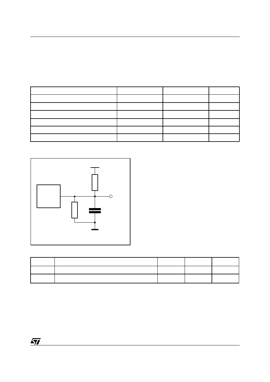
Figure 5. AC Testing Load Circuit
Table 4. Capacitance
Note: 1. Effective capacitance measured with power supply at 5V. Sampled only, not 100% tested.
2. At 25∞C, f = 1MHz.
3. Outputs deselected.
Parameter
M48T02
M48T12
Unit
Supply Voltage (V
CC
)
4.75 to 5.5
4.5 to 5.5
V
Ambient Operating Temperature (T
A
)
0 to 70
0 to 70
∞C
Load Capacitance (C
L
)
100
100
pF
Input Rise and Fall Times
5
5
ns
Input Pulse Voltages
0 to 3
0 to 3
V
Input and Output Timing Ref. Voltages
1.5
1.5
V
AI01019
5V
OUT
CL = 100pF
CL includes JIG capacitance
1.8k
DEVICE
UNDER
TEST
1k
Symbol
Parameter
(1,2)
Min
Max
Unit
C
IN
Input Capacitance
10
pF
C
IO
(3)
Input / Output Capacitance
10
pF