
1/26
March 2003
Rev. 4.0
M48T08
M48T08Y, M48T18
5V, 64 Kbit (8 Kb x 8) TIMEKEEPER
Æ
SRAM
FEATURES SUMMARY
s
INTEGRATED ULTRA LOW POWER SRAM,
REAL TIME CLOCK, POWER-FAIL CONTROL
CIRCUIT, and BATTERY
s
BYTEWIDETM RAM-LIKE CLOCK ACCESS
s
BCD CODED YEAR, MONTH, DAY, DATE,
HOURS, MINUTES, and SECONDS
s
TYPICAL CLOCK ACCURACY OF ±1 MINUTE
A MONTH, AT 25∞C
s
AUTOMATIC POWER-FAIL CHIP DESELECT
and WRITE PROTECTION
s
WRITE PROTECT VOLTAGES
(V
PFD
= Power-fail Deselect Voltage):
≠ M48T08: V
CC
= 4.75 to 5.5V
4.5V
V
PFD
4.75V
≠ M48T18/T08Y: V
CC
= 4.5 to 5.5V
4.2V
V
PFD
4.5V
s
SOFTWARE CONTROLLED CLOCK
CALIBRATION FOR HIGH ACCURACY
APPLICATIONS
s
SELF-CONTAINED BATTERY and CRYSTAL
IN THE CAPHATTM DIP PACKAGE
s
PACKAGING INCLUDES A 28-LEAD SOIC and
SNAPHAT
Æ
TOP
s
(to be Ordered Separately)
s
SOIC PACKAGE PROVIDES DIRECT
CONNECTION FOR A SNAPHAT TOP WHICH
CONTAINS THE BATTERY and CRYSTAL
s
PIN and FUNCTION COMPATIBLE WITH
DS1643 and JEDEC STANDARD 8K x 8
SRAMs
Figure 1. 28-pin PCDIP, CAPHATTM Package
Figure 2. 28-pin SOIC Package
28
1
PCDIP28 (PC)
Battery/Crystal
CAPHAT
28
1
SNAPHAT (SH)
Battery/Crystal
SOH28 (MH)

M48T08, M48T18, M48T08Y
2/26
TABLE OF CONTENTS
SUMMARY DESCRIPTION . . . . . . . . . . . . . . . . . . . . . . . . . . . . . . . . . . . . . . . . . . . . . . . . . . . . . . . . . . . 3
Figure 3. Logic Diagram . . . . . . . . . . . . . . . . . . . . . . . . . . . . . . . . . . . . . . . . . . . . . . . . . . . . . . . . . . 3
Table 1. Signal Names . . . . . . . . . . . . . . . . . . . . . . . . . . . . . . . . . . . . . . . . . . . . . . . . . . . . . . . . . . . 3
Figure 4. DIP Connections . . . . . . . . . . . . . . . . . . . . . . . . . . . . . . . . . . . . . . . . . . . . . . . . . . . . . . . . 4
Figure 5. SOIC Connections . . . . . . . . . . . . . . . . . . . . . . . . . . . . . . . . . . . . . . . . . . . . . . . . . . . . . . . 4
Figure 6. Block Diagram . . . . . . . . . . . . . . . . . . . . . . . . . . . . . . . . . . . . . . . . . . . . . . . . . . . . . . . . . . 4
MAXIMUM RATING. . . . . . . . . . . . . . . . . . . . . . . . . . . . . . . . . . . . . . . . . . . . . . . . . . . . . . . . . . . . . . . . . 5
Table 2. Absolute Maximum Ratings . . . . . . . . . . . . . . . . . . . . . . . . . . . . . . . . . . . . . . . . . . . . . . . . . 5
DC AND AC PARAMETERS. . . . . . . . . . . . . . . . . . . . . . . . . . . . . . . . . . . . . . . . . . . . . . . . . . . . . . . . . . 6
Table 3. Operating and AC Measurement Conditions . . . . . . . . . . . . . . . . . . . . . . . . . . . . . . . . . . . . 6
Figure 7. AC Testing Load Circuit . . . . . . . . . . . . . . . . . . . . . . . . . . . . . . . . . . . . . . . . . . . . . . . . . . . 6
Table 4. Capacitance. . . . . . . . . . . . . . . . . . . . . . . . . . . . . . . . . . . . . . . . . . . . . . . . . . . . . . . . . . . . . 6
Table 5. DC Characteristics. . . . . . . . . . . . . . . . . . . . . . . . . . . . . . . . . . . . . . . . . . . . . . . . . . . . . . . . 7
OPERATION MODES . . . . . . . . . . . . . . . . . . . . . . . . . . . . . . . . . . . . . . . . . . . . . . . . . . . . . . . . . . . . . . . 8
Table 6. Operating Modes . . . . . . . . . . . . . . . . . . . . . . . . . . . . . . . . . . . . . . . . . . . . . . . . . . . . . . . . . 8
READ Mode . . . . . . . . . . . . . . . . . . . . . . . . . . . . . . . . . . . . . . . . . . . . . . . . . . . . . . . . . . . . . . . . . . . 9
Figure 8. READ Mode AC Waveforms . . . . . . . . . . . . . . . . . . . . . . . . . . . . . . . . . . . . . . . . . . . . . . . 9
Table 7. READ Mode AC Characteristics . . . . . . . . . . . . . . . . . . . . . . . . . . . . . . . . . . . . . . . . . . . . 10
WRITE Mode. . . . . . . . . . . . . . . . . . . . . . . . . . . . . . . . . . . . . . . . . . . . . . . . . . . . . . . . . . . . . . . . . . 11
Figure 9. WRITE Enable Controlled, WRITE AC Waveform . . . . . . . . . . . . . . . . . . . . . . . . . . . . . . 11
Figure 10. Chip Enable Controlled, WRITE AC Waveforms . . . . . . . . . . . . . . . . . . . . . . . . . . . . . . 12
Table 8. WRITE Mode AC Characteristics . . . . . . . . . . . . . . . . . . . . . . . . . . . . . . . . . . . . . . . . . . . 13
Data Retention Mode . . . . . . . . . . . . . . . . . . . . . . . . . . . . . . . . . . . . . . . . . . . . . . . . . . . . . . . . . . . 14
Figure 11. Power Down/Up Mode AC Waveforms . . . . . . . . . . . . . . . . . . . . . . . . . . . . . . . . . . . . . 14
Table 9. Power Down/Up AC Characteristics . . . . . . . . . . . . . . . . . . . . . . . . . . . . . . . . . . . . . . . . . 15
Table 10. Power Down/Up Trip Points DC Characteristics . . . . . . . . . . . . . . . . . . . . . . . . . . . . . . . 15
CLOCK OPERATIONS . . . . . . . . . . . . . . . . . . . . . . . . . . . . . . . . . . . . . . . . . . . . . . . . . . . . . . . . . . . . . 16
Reading the Clock . . . . . . . . . . . . . . . . . . . . . . . . . . . . . . . . . . . . . . . . . . . . . . . . . . . . . . . . . . . . . 16
Setting the Clock . . . . . . . . . . . . . . . . . . . . . . . . . . . . . . . . . . . . . . . . . . . . . . . . . . . . . . . . . . . . . . 16
Table 11. Register Map . . . . . . . . . . . . . . . . . . . . . . . . . . . . . . . . . . . . . . . . . . . . . . . . . . . . . . . . . . 16
Stopping and Starting the Oscillator . . . . . . . . . . . . . . . . . . . . . . . . . . . . . . . . . . . . . . . . . . . . . . 17
Calibrating the Clock. . . . . . . . . . . . . . . . . . . . . . . . . . . . . . . . . . . . . . . . . . . . . . . . . . . . . . . . . . . 17
Figure 12. Crystal Accuracy Across Temperature . . . . . . . . . . . . . . . . . . . . . . . . . . . . . . . . . . . . . . 18
Figure 13. Clock Calibration . . . . . . . . . . . . . . . . . . . . . . . . . . . . . . . . . . . . . . . . . . . . . . . . . . . . . . 18
V
CC
Noise And Negative Going Transients. . . . . . . . . . . . . . . . . . . . . . . . . . . . . . . . . . . . . . . . . 19
Figure 14. Supply Voltage Protection . . . . . . . . . . . . . . . . . . . . . . . . . . . . . . . . . . . . . . . . . . . . . . . 19
PACKAGE MECHANICAL INFORMATION . . . . . . . . . . . . . . . . . . . . . . . . . . . . . . . . . . . . . . . . . . . . . 20
PART NUMBERING . . . . . . . . . . . . . . . . . . . . . . . . . . . . . . . . . . . . . . . . . . . . . . . . . . . . . . . . . . . . . . . 24
Table 17. SNAPHAT Battery Table . . . . . . . . . . . . . . . . . . . . . . . . . . . . . . . . . . . . . . . . . . . . . . . . . 24
REVISION HISTORY. . . . . . . . . . . . . . . . . . . . . . . . . . . . . . . . . . . . . . . . . . . . . . . . . . . . . . . . . . . . . . . 25
3/26
M48T08, M48T18, M48T08Y
SUMMARY DESCRIPTION
The M48T08/18/08Y TIMEKEEPER
Æ
RAM is an
8K x 8 non-volatile static RAM and real time clock
which is pin and functional compatible with the
DS1643. The monolithic chip is available in two
special packages to provide a highly integrated
battery backed-up memory and real time clock so-
lution.
The M48T08/18/08Y is a non-volatile pin and func-
tion equivalent to any JEDEC standard 8K x 8
SRAM. It also easily fits into many ROM, EPROM,
and EEPROM sockets, providing the non-volatility
of PROMs without any requirement for special
WRITE timing or limitations on the number of
WRITEs that can be performed.
The 28-pin, 600mil DIP CAPHATTM houses the
M48T08/18/08Y silicon with a quartz crystal and a
long- life lithium button cell in a single package.
The 28-pin, 330mil SOIC provides sockets with
gold plated contacts at both ends for direct con-
nection to a separate SNAPHAT
Æ
housing con-
taining the battery and crystal. The unique design
allows the SNAPHAT battery package to be
mounted on top of the SOIC package after the
completion of the surface mount process. Inser-
tion of the SNAPHAT housing after reflow pre-
vents potential battery and crystal damage due to
the high temperatures required for device surface-
mounting. The SNAPHAT housing is keyed to pre-
vent reverse insertion.
The SOIC and battery/crystal packages are
shipped separately in plastic anti-static tubes or in
Tape & Reel form. For the 28 lead SOIC, the bat-
tery/crystal package (e.g., SNAPHAT) part num-
ber is "M4T28-BR12SH" or "M4T32-BR12SH"
(see Table 17, page 24).
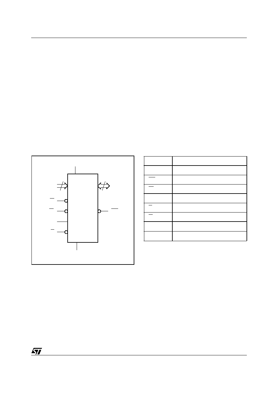
Figure 3. Logic Diagram
Table 1. Signal Names
AI01020
13
A0-A12
W
DQ0-DQ7
VCC
M48T08
M48T08Y
M48T18
G
E2
VSS
8
E1
INT
A0-A12
Address Inputs
DQ0-DQ7
Data Inputs / Outputs
INT
Power Fail Interrupt (Open Drain)
E1
Chip Enable 1
E2
Chip Enable 2
G
Output Enable
W
WRITE Enable
V
CC
Supply Voltage
V
SS
Ground
5/26
M48T08, M48T18, M48T08Y
MAXIMUM RATING
Stressing the device above the rating listed in the
"Absolute Maximum Ratings" table may cause
permanent damage to the device. These are
stress ratings only and operation of the device at
these or any other conditions above those indicat-
ed in the Operating sections of this specification is
not implied. Exposure to Absolute Maximum Rat-
ing conditions for extended periods may affect de-
vice reliability. Refer also to the
STMicroelectronics SURE Program and other rel-
evant quality documents.
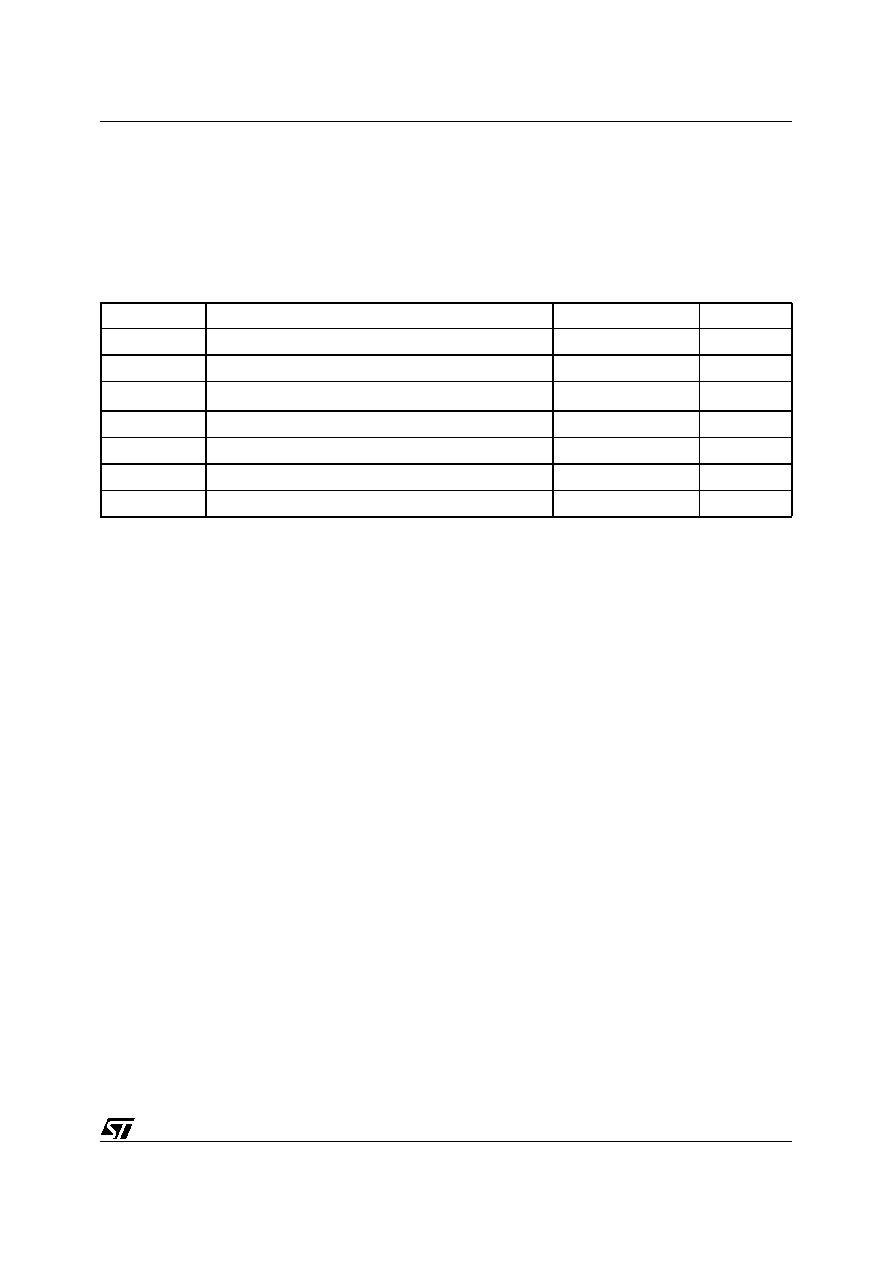
Table 2. Absolute Maximum Ratings
Note: 1. For DIP package: Soldering temperature not to exceed 260∞C for 10 seconds (total thermal budget not to exceed 150∞C for longer
than 30 seconds).
2. For SO package: Reflow at peak temperature of 215∞C to 225∞C for < 60 seconds (total thermal budget not to exceed 180∞C for
between 90 to 120 seconds).
CAUTION: Negative undershoots below ≠0.3V are not allowed on any pin while in the Battery Back-up mode.
CAUTION: Do NOT wave solder SOIC to avoid damaging SNAPHAT sockets.
Symbol
Parameter
Value
Unit
T
A
Ambient Operating Temperature
0 to 70
∞C
T
STG
Storage Temperature (V
CC
Off, Oscillator Off)
≠40 to 85
∞C
T
SLD
(1,2)
Lead Solder Temperature for 10 seconds
260
∞C
V
IO
Input or Output Voltages
≠0.3 to 7
V
V
CC
Supply Voltage
≠0.3 to 7
V
I
O
Output Current
20
mA
P
D
Power Dissipation
1
W
