1/33
September 2004
M48T201Y
M48T201V
5.0 or 3.3V TIMEKEEPER
Æ
Supervisor
FEATURES SUMMARY
CONVERTS LOW POWER SRAM INTO
NVRAMs
YEAR 2000 COMPLIANT
BATTERY LOW FLAG
INTEGRATED REAL TIME CLOCK, POWER-
FAIL CONTROL CIRCUIT, BATTERY AND
CRYSTAL
WATCHDOG TIMER
CHOICE OF WRITE PROTECT VOLTAGES
(V
PFD
= Power-fail Deselect Voltage):
≠
M48T201Y: V
CC
= 4.5 to 5.5V
4.1V
V
PFD
4.5V
≠
M48T201V: V
CC
= 3.0 to 3.6V
2.7V
V
PFD
3.0V
MICROPROCESSOR POWER-ON RESET
(Valid even during battery back-up mode.)
PROGRAMMABLE ALARM OUTPUT
ACTIVE IN THE BATTERY BACKED-UP
MODE
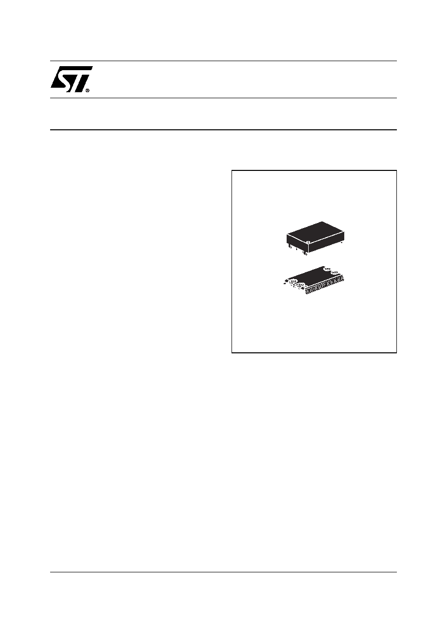
PACKAGING INCLUDES A 44-LEAD SOIC
AND SNAPHAT
Æ
TOP (to be ordered
separately)
SOIC PACKAGE PROVIDES DIRECT
CONNECTION FOR A SNAPHAT
Æ
TOP
WHICH CONTAINS THE BATTERY AND
CRYSTAL
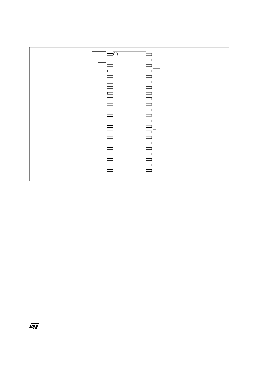
Figure 1. Package
SOH44 (MH)
44-pin SOIC
SNAPHAT (SH)
Crystal/Battery
44
1

M48T201Y, M48T201V
2/33
TABLE OF CONTENTS
FEATURES SUMMARY . . . . . . . . . . . . . . . . . . . . . . . . . . . . . . . . . . . . . . . . . . . . . . . . . . . . . . . . . . . . . 1
Figure 1. Package. . . . . . . . . . . . . . . . . . . . . . . . . . . . . . . . . . . . . . . . . . . . . . . . . . . . . . . . . . . . . . . 1
DESCRIPTION . . . . . . . . . . . . . . . . . . . . . . . . . . . . . . . . . . . . . . . . . . . . . . . . . . . . . . . . . . . . . . . . . . . . 4
Figure 2. Logic Diagram . . . . . . . . . . . . . . . . . . . . . . . . . . . . . . . . . . . . . . . . . . . . . . . . . . . . . . . . . . 4
Table 1. Signal Names . . . . . . . . . . . . . . . . . . . . . . . . . . . . . . . . . . . . . . . . . . . . . . . . . . . . . . . . . . 4
Figure 3. SOIC Connections . . . . . . . . . . . . . . . . . . . . . . . . . . . . . . . . . . . . . . . . . . . . . . . . . . . . . . . 5
Figure 4. Hardware Hookup . . . . . . . . . . . . . . . . . . . . . . . . . . . . . . . . . . . . . . . . . . . . . . . . . . . . . . . 6
OPERATION . . . . . . . . . . . . . . . . . . . . . . . . . . . . . . . . . . . . . . . . . . . . . . . . . . . . . . . . . . . . . . . . . . . . . . 7
Address Decoding . . . . . . . . . . . . . . . . . . . . . . . . . . . . . . . . . . . . . . . . . . . . . . . . . . . . . . . . . . . . . . 7
Table 2. Operating Modes . . . . . . . . . . . . . . . . . . . . . . . . . . . . . . . . . . . . . . . . . . . . . . . . . . . . . . . . 7
READ Mode . . . . . . . . . . . . . . . . . . . . . . . . . . . . . . . . . . . . . . . . . . . . . . . . . . . . . . . . . . . . . . . . . . . 8
Figure 5. G
CON
Timing When Switching Between RTC and External SRAM . . . . . . . . . . . . . . . . . . 8
Figure 6. READ Cycle Timing: RTC and External RAM Control Signals . . . . . . . . . . . . . . . . . . . . . 9
Table 3. READ Mode AC Characteristics . . . . . . . . . . . . . . . . . . . . . . . . . . . . . . . . . . . . . . . . . . . 10
WRITE Mode. . . . . . . . . . . . . . . . . . . . . . . . . . . . . . . . . . . . . . . . . . . . . . . . . . . . . . . . . . . . . . . . . . 11
Figure 7. WRITE Cycle Timing: RTC & External RAM Control Signals . . . . . . . . . . . . . . . . . . . . . 11
Table 4. WRITE Mode AC Characteristics . . . . . . . . . . . . . . . . . . . . . . . . . . . . . . . . . . . . . . . . . . 12
Data Retention Mode . . . . . . . . . . . . . . . . . . . . . . . . . . . . . . . . . . . . . . . . . . . . . . . . . . . . . . . . . . . 13
CLOCK OPERATION . . . . . . . . . . . . . . . . . . . . . . . . . . . . . . . . . . . . . . . . . . . . . . . . . . . . . . . . . . . . . . 14
TIMEKEEPERÆ Registers . . . . . . . . . . . . . . . . . . . . . . . . . . . . . . . . . . . . . . . . . . . . . . . . . . . . . . . 14
Reading the Clock . . . . . . . . . . . . . . . . . . . . . . . . . . . . . . . . . . . . . . . . . . . . . . . . . . . . . . . . . . . . . 14
Setting the Clock . . . . . . . . . . . . . . . . . . . . . . . . . . . . . . . . . . . . . . . . . . . . . . . . . . . . . . . . . . . . . . 14
Stopping and Starting the Oscillator . . . . . . . . . . . . . . . . . . . . . . . . . . . . . . . . . . . . . . . . . . . . . . 14
Table 5. TIMEKEEPERÆ Register Map . . . . . . . . . . . . . . . . . . . . . . . . . . . . . . . . . . . . . . . . . . . . 15
Setting the Alarm Clock . . . . . . . . . . . . . . . . . . . . . . . . . . . . . . . . . . . . . . . . . . . . . . . . . . . . . . . . 16
Figure 8. Alarm Interrupt Reset Waveforms . . . . . . . . . . . . . . . . . . . . . . . . . . . . . . . . . . . . . . . . . . 16
Table 6. Alarm Repeat Modes . . . . . . . . . . . . . . . . . . . . . . . . . . . . . . . . . . . . . . . . . . . . . . . . . . . . 16
Figure 9. Back-up Mode Alarm Waveforms . . . . . . . . . . . . . . . . . . . . . . . . . . . . . . . . . . . . . . . . . . 17
Watchdog Timer . . . . . . . . . . . . . . . . . . . . . . . . . . . . . . . . . . . . . . . . . . . . . . . . . . . . . . . . . . . . . . 17
Square Wave Output . . . . . . . . . . . . . . . . . . . . . . . . . . . . . . . . . . . . . . . . . . . . . . . . . . . . . . . . . . . 18
Table 7. Square Wave Output Frequency . . . . . . . . . . . . . . . . . . . . . . . . . . . . . . . . . . . . . . . . . . . 18
Power-on Reset . . . . . . . . . . . . . . . . . . . . . . . . . . . . . . . . . . . . . . . . . . . . . . . . . . . . . . . . . . . . . . . 19
Reset Inputs (RSTIN1 & RSTIN2) . . . . . . . . . . . . . . . . . . . . . . . . . . . . . . . . . . . . . . . . . . . . . . . . . 19
Figure 10.RSTIN1 and RSTIN2 Timing Waveforms . . . . . . . . . . . . . . . . . . . . . . . . . . . . . . . . . . . . 19
Table 8. Reset AC Characteristics. . . . . . . . . . . . . . . . . . . . . . . . . . . . . . . . . . . . . . . . . . . . . . . . . 19
Calibrating the Clock. . . . . . . . . . . . . . . . . . . . . . . . . . . . . . . . . . . . . . . . . . . . . . . . . . . . . . . . . . . 20
Figure 11.Crystal Accuracy Across Temperature . . . . . . . . . . . . . . . . . . . . . . . . . . . . . . . . . . . . . . 21
Figure 12.Calibration Waveform . . . . . . . . . . . . . . . . . . . . . . . . . . . . . . . . . . . . . . . . . . . . . . . . . . . 21
Battery Low Warning. . . . . . . . . . . . . . . . . . . . . . . . . . . . . . . . . . . . . . . . . . . . . . . . . . . . . . . . . . . 22
Initial Power-on Defaults. . . . . . . . . . . . . . . . . . . . . . . . . . . . . . . . . . . . . . . . . . . . . . . . . . . . . . . . 22

3/33
M48T201Y, M48T201V
Table 9. Default Values . . . . . . . . . . . . . . . . . . . . . . . . . . . . . . . . . . . . . . . . . . . . . . . . . . . . . . . . . 22
V
CC
Noise And Negative Going Transients. . . . . . . . . . . . . . . . . . . . . . . . . . . . . . . . . . . . . . . . . 23
Figure 13.Supply Voltage Protection . . . . . . . . . . . . . . . . . . . . . . . . . . . . . . . . . . . . . . . . . . . . . . . . 23
MAXIMUM RATING. . . . . . . . . . . . . . . . . . . . . . . . . . . . . . . . . . . . . . . . . . . . . . . . . . . . . . . . . . . . . . . . 24
Table 10. Absolute Maximum Ratings . . . . . . . . . . . . . . . . . . . . . . . . . . . . . . . . . . . . . . . . . . . . . . . 24
DC AND AC PARAMETERS. . . . . . . . . . . . . . . . . . . . . . . . . . . . . . . . . . . . . . . . . . . . . . . . . . . . . . . . . 25
Table 11. DC and AC Measurement Conditions . . . . . . . . . . . . . . . . . . . . . . . . . . . . . . . . . . . . . . . 25
Figure 14.AC Testing Load Circuit . . . . . . . . . . . . . . . . . . . . . . . . . . . . . . . . . . . . . . . . . . . . . . . . . 25
Table 12. Capacitance. . . . . . . . . . . . . . . . . . . . . . . . . . . . . . . . . . . . . . . . . . . . . . . . . . . . . . . . . . . 25
Table 13. DC Characteristics. . . . . . . . . . . . . . . . . . . . . . . . . . . . . . . . . . . . . . . . . . . . . . . . . . . . . . 26
Figure 15.Power Down/Up Mode AC Waveforms . . . . . . . . . . . . . . . . . . . . . . . . . . . . . . . . . . . . . . 27
Table 14. Power Down/Up Mode AC Characteristics . . . . . . . . . . . . . . . . . . . . . . . . . . . . . . . . . . . 27
PACKAGE MECHANICAL INFORMATION . . . . . . . . . . . . . . . . . . . . . . . . . . . . . . . . . . . . . . . . . . . . . 28
Figure 16.SOH44 ≠ 44-lead Plastic Small Outline, SNAPHAT, Package Outline . . . . . . . . . . . . . . 28
Table 15. SOH44 ≠ 44-lead Plastic Small Outline, SNAPHAT, Package Mechanical Data . . . . . . 28
Figure 17.SH ≠ 4-pin SNAPHAT Housing for 48mAh Battery & Crystal, Package Outline . . . . . . . 29
Table 16. SH ≠ 4-pin SNAPHAT Housing for 48mAh Battery & Crystal, Package Mech. Data. . . . 29
Figure 18.SH ≠ 4-pin SNAPHAT Housing for 120mAh Battery & Crystal, Package Outline . . . . . . 30
Table 17. SH ≠ 4-pin SNAPHAT Housing for 120mAh Battery & Crystal, Package Mech. Data. . . 30
PART NUMBERING . . . . . . . . . . . . . . . . . . . . . . . . . . . . . . . . . . . . . . . . . . . . . . . . . . . . . . . . . . . . . . . 31
Table 18. Ordering Information Example. . . . . . . . . . . . . . . . . . . . . . . . . . . . . . . . . . . . . . . . . . . . . 31
Table 19. SNAPHATÆ Battery Table. . . . . . . . . . . . . . . . . . . . . . . . . . . . . . . . . . . . . . . . . . . . . . . . 31
REVISION HISTORY. . . . . . . . . . . . . . . . . . . . . . . . . . . . . . . . . . . . . . . . . . . . . . . . . . . . . . . . . . . . . . . 32
Table 20. Document Revision History . . . . . . . . . . . . . . . . . . . . . . . . . . . . . . . . . . . . . . . . . . . . . . . 32
M48T201Y, M48T201V
4/33
DESCRIPTION
The M48T201Y/V are self-contained devices that
include a real time clock (RTC), programmable
alarms, a watchdog timer, and a square wave out-
put which provides control of up to 512K x 8 of ex-
ternal low-power static RAM. Access to all RTC
functions and the external RAM is the same as
conventional bytewide SRAM. The 16 TIME-
KEEPER
Æ
registers offer year, month, date, day,
hour, minute, second, calibration, alarm, century,
watchdog, and square wave output data. External-
ly attached static RAMs are controlled by the
M48T201Y/V via the G
CON
and E
CON
signals.
The 44-pin, 330mil SOIC provides sockets with
gold plated contacts at both ends for direct con-
nection to a separate SNAPHAT
Æ
housing con-
taining the battery and crystal. The unique design
allows the SNAPHAT battery package to be
mounted on top of the SOIC package after the
completion of the surface mount process.
Insertion of the SNAPHAT housing after reflow
prevents potential battery damage due to the high
temperatures required for device surface-mount-
ing. The SNAPHAT housing is keyed to prevent
reverse insertion. The SOIC and battery packages
are shipped separately in plastic anti-static tubes
or in Tape & Reel form. For the 44-lead SOIC, the
battery/crystal package (e.g., SNAPHAT) part
number is "M4Txx-BR12SH" (see
Table
19., page 31
).
Caution: Do not place the SNAPHAT battery/crys-
tal top in conductive foam as this will drain the lith-
ium button-cell battery.
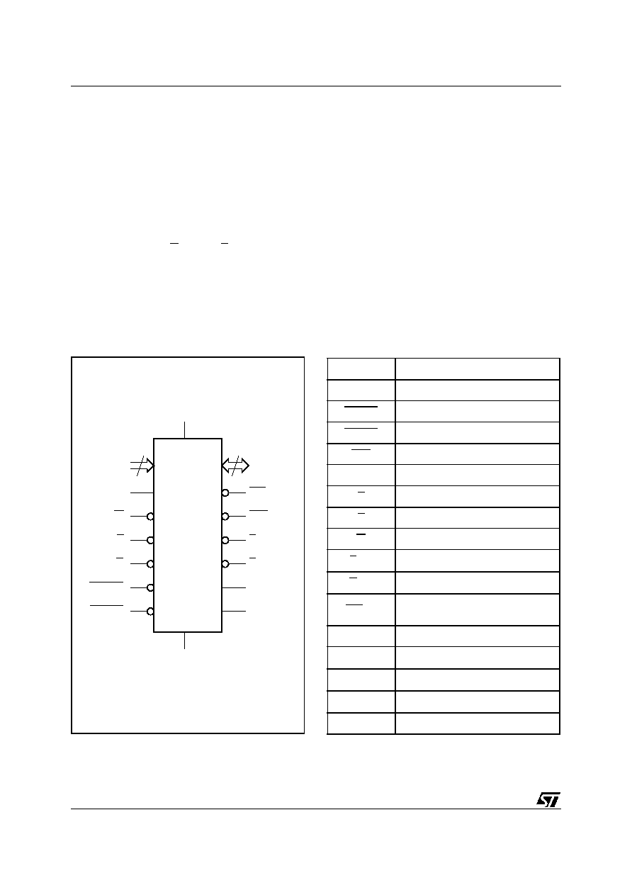
Figure 2. Logic Diagram
Table 1. Signal Names
AI02240
19
A0-A18
WDI
DQ0-DQ7
VCC
M48T201Y
M48T201V
G
VSS
8
E
ECON
GCON
W
RSTIN2
RSTIN1
RST
IRQ/FT
VOUT
SQW
A0-A18
Address Inputs
DQ0-DQ7
Data Inputs / Outputs
RSTIN1
Reset 1 Input
RSTIN2
Reset 2 Input
RST
Reset Output (Open Drain)
WDI
Watchdog Input
E
Chip Enable Input
G
Output Enable Input
W
WRITE Enable Input
E
CON
RAM Chip Enable Output
G
CON
RAM Enable Output
IRQ/FT
Interrupt / Frequency Test Output
(Open Drain)
SQW
Square Wave Output
V
OUT
Supply Voltage Output
V
CC
Supply Voltage
V
SS
Ground
NC
Not Connected Internally